1962 Journal of The Electrochemical Society, 147 (5) 1962-1964 (2000) S0013-4651(99)10-038-7 CCC: $7.00 © The Electrochemical Society, Inc.
Gate oxide integrity1-4is one of the most important factors for integrating SiGe p-metal oxide semiconductor field effect transistors (p-MOSFET) into current complementary metal oxide semiconduc-tor (CMOS) technology, even though SiGe itself exhibits higher hole mobility, improved current drive capability, and increased packaging density of CMOS circuits. Unfortunately, in spite of the maturely developed SiGe material, the growth of high-quality oxide is still the major challenge for SiGe p-MOSFET. The main issue for achieving high-quality gate oxide is that direct thermal oxidation produces a mixed SiO2and GeOxwith degraded oxide quality.5-7Furthermore, Ge pileup in the oxide/Si interface is also believed to severely in-crease the interface trap density. To overcome these problems men-tioned above, low-temperature radio-frequency (rf) plasma8 and electron cyclotron resonance9,10techniques are proposed for SiGe oxidation. Although accompanying H2O vapor anneal favors accept-able interface trap and fixed charge density, it is still difficult to achieve comparable oxide breakdown electric field as conventional thermal oxide and the gate oxide integrity is suspected to degrade by plasma damage. Another technique employs an Si cap layer on SiGe with subsequent plasma-enhanced chemical vapor deposited oxide or low-temperature oxidation (700-7508C).11-14 Although good oxide charge and interface trap densities are reported, unfortunately, the low-temperature constraint may not only degrade the oxide reli-ability but also prohibits the source-drain implant activation that will increase both contact resistance and junction leakage.15In this work, we propose a simple and inexpensive approach to form high-quality gate oxide on high-temperature-formed Si0.6Ge0.4. Because our SiGe is formed by solid phase epitaxy at high temperatures, no low-tem-perature processing restriction would be imposed and conventional thermal oxidation can be directly applied. To further ensure good oxide integrity, a ,30 Å Si top layer is formed on Si0.6Ge0.4for ther-mal oxidation. Good oxide quality of 50 Å is evidenced by the com-parable properties to conventional Si dioxide (SiO2) such as leakage current, breakdown electric field, charge-to-breakdown (QBD), inter-face trap density, and small stress-induced leakage current (SILC). The biggest advantage of the formed SiGe MOS structure is that its process is completely compatible to current very large scale integra-tion (VLSI) technology.
Experimental
4 in. p-type Si(100) wafers were used in this work with a resis-tivity of 10 V cm. The wafer were cleaned in a 3:1 solution of H2SO4 and H2O2, a high-purity deionized (DI) water rinse, a 1% HF etch, a DI water rinse, and a final HF vapor passivation. MOS capacitors were fabricated to characterize the oxide quality. After device isola-tion with a 3000 Å field oxide, a 350 Å SiGe layer with good crys-talline quality was first formed in the active region by solid phase epitaxy at 9008C using rapid thermal annealing (RTA). In fact, this
process is very similar to form single crystalline CoSi2 on Si. 16 More detailed material characterization can be found in our previous study.17,18An amorphous Si is then deposited on the SiGe layer and subsequent 9008C RTA is applied to form the 30 Å Si top layer by solid phase epitaxy. Before gate oxidation, wafers were cleaned again with standard RCA process to avoid any contamination that will strongly affect the oxide quality. Gate oxides of 50 Å were grown by dry O2at 9008C followed by a 3000 Å poly-Si deposition with the subsequent n-type doping by phosphorus. Standard contact is formed by aluminum sputtering and sintered at 4008C for 30 min in forming gas. In addition to thermal oxides grown on Si/SiGe, con-trol thermal SiO2was also fabricated as references. We have used X-ray diffraction (XRD) to characterize the crystal structure and composition of SiGe. The surface roughness before and after oxida-tion was observed by atomic force microscopy (AFM). The gate oxide integrity was electrically examined by capacitance-voltage (C-V) measurements, current-voltage (I-V) characteristics, time-dependent dielectric breakdown (TDDB), QBD, and SILC.
Results and Discussion
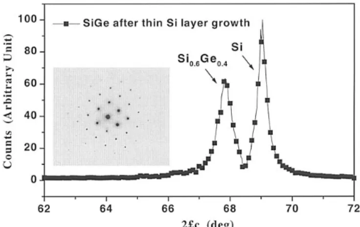
We first characterized the composition and material quality of the 30 Å Si/350 Å SiGe by measuring XRD spectra shown in Fig. 1. The composition of this SiGe layer is obtained from its relative peak position to Si and a 40% Ge is calculated in the alloy. The strong and sharp diffracted peak comparable to Si indicates a single crystalline behavior with good SiGe material quality. The inset picture is the electron diffraction pattern of this structure. By examining the high-er-order reflections, we found the diffraction spots resulting from SiGe and Si are well aligned, which proves the epitaxial nature of
High-Quality Thermal Oxide Grown on High-Temperature-Formed SiGe
Y. H. Wu,
aS. B. Chen,
aA. Chin,
a,zand W. J. Chen
baDepartment of Electronics Engineering, National Chiao Tung University, Hsinchu, Taiwan
bDepartment of Mechanical Materials Engineering, National Yun-Lin Polytechnic Institute, Huwei, Taiwan
We have developed a high-quality gate oxide on Si0.6Ge0.4with a 30 Å Si top layer. The good oxide integrity comparable to con-ventional thermal oxide is demonstrated by the low interface trap density of 6.2 3 1010eV21cm22, low oxide charge of 5.8 3 1010cm22, small leakage current at 3.3 V of 4.2 3 1028A/cm2, high breakdown field of 13.8 MV/cm, good charge-to-breakdown of 5.2 C/cm2, and small stress-induced leakage current. This good oxide integrity is directly related to our previously developed SiGe formed by solid phase epitaxy at high temperatures that is stable during thermal oxidation. This simple process is fully com-patible with existing very large scale integration technology.
© 2000 The Electrochemical Society. S0013-4651(99)10-038-7. All rights reserved. Manuscript submitted October 8, 1999; revised manuscript received January 13, 2000.
z E-mail: [email protected]
Figure 1. XRD of SiGe and Si substrate after a thin Si layer growth. The nar-row linewidth of SiGe compatible to Si suggests good material quality. Inset: the related electron diffraction pattern.
) unless CC License in place (see abstract).
ecsdl.org/site/terms_use
address. Redistribution subject to ECS terms of use (see
140.113.38.11
Journal of The Electrochemical Society, 147 (5) 1962-1964 (2000) 1963 S0013-4651(99)10-038-7 CCC: $7.00 © The Electrochemical Society, Inc.
this heterostructure. The highly oriented diffraction pattern is also consistent with the sharp and strong XRD peak that indicates the formed SiGe has good crystalline quality. It is important to notice that the top Si should be single crystal although the oxidized SiO2is amorphous. This is because electron or hole wave function19may occupy both SiGe and unconsumed top Si that can degrade the device interface and transport property due to the poor quality of amorphous Si as the case of thin film transistor.
We used C-V measurements to investigate the oxide quality. Fig-ure 2a shows the typical C-V curves of the Si/Si0.6Ge0.4MOS capac-itor with a 50 Å oxide. The curve clearly shows no anomalous phe-nomenon such as sequential population of Si0.6Ge0.4channel and top Si layer.11This is because the thin top Si layer is almost fully con-sumed during thermal oxidation. The closely matched curves meas-ured at high and low frequency under accumulation suggests good interface property with a very low trap density. We have further plot-ted the calculaplot-ted interface-trap density in Fig. 2b obtained from the C-V curves. A low interface and oxide charge density of 6.2 3 1010eV21cm22and of 5.8 3 1010cm22are measured, respective-ly, which indicates the good oxide quality similar to thermal SiO2 and are acceptable for practical VLSI technology.
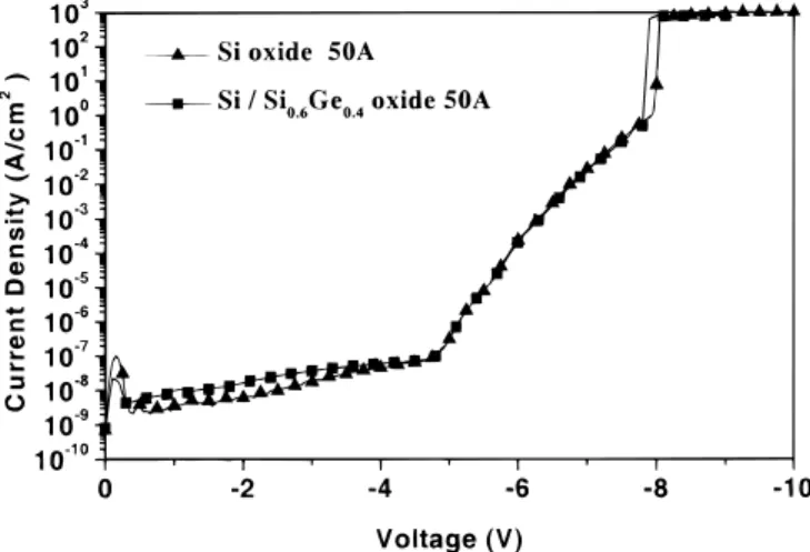
We have also studied the oxide leakage current and breakdown behavior. Figure 3 shows the I-V characteristics of 50 Å thermal oxides grown on both Si/Si0.6Ge0.4and Si. The small current peak at low voltage (<0.5 V) is due to the neutral trap conduction distributed in the oxide. It is important to note that the oxide grown on Si/ Si0.6Ge0.4has comparable electrical characteristics with Si control sample. This is because the thermal oxide is grown on top Si layer rather than directly on SiGe that circumambulates the problems of forming a mixed SiO2and GeOxwith Ge snow plowing and
accumu-lated at oxide/SiGe interface.9Nevertheless, the slightly higher leak-age current and lower breakdown voltleak-age may be due to the inferior crystalline quality of the top Si layer to bulk Si. A respective break-down electric field and leakage current at 23.3 V of 13.8 MV/cm and 4.2 3 1028 A/cm2 are measured for thermal oxide grown on Si/ Si0.6Ge0.4, which is also capable for current VLSI application.
Gate oxide reliability is another important factor for practical applications. Figure 4 shows the cumulative failure plot on TDDB lifetime under a constant voltage stress at 26.5 V. A negative polar-ity was used in this measurement to avoid any voltage drop in the depletion region. The inset figure shows the time evolution of gate current under this stress voltage. It shows that there was a gradual decrease of oxide current with time until the oxide undergoes a dielectric breakdown and QBDcan be calculated from this plot. The
QBDobtained under this condition is in the range of 5.1 to 6.7 C/cm2 for the control Si sample and 4.5 to 5.9 C/cm2for oxide grown on Si/Si0.6Ge0.4. The tight distribution and comparable TDDB and QBD values with control thermal SiO2suggest the excellent reliability of Si/Si0.6Ge0.4oxide.
We also measured the SILC to further examine the oxide quality because it is important for gate oxide reliability and those devices with carrier transport through oxide such as flash memory. Figure 5 shows the SILC of oxide grown on Si/Si0.6Ge0.4and the inset figure is the tunneling current under 25 V stress for 10000 s. The tiny in-crease of leakage current also proves good SILC resistance of ther-mal oxide grown on Si/Si0.6Ge0.4. This small SILC effect on oxide is also consistent with the high breakdown electric field, QBD, and TDDB mentioned previously.
Figure 2. (a) Low- and high-frequency C-V curves and (b) interface-trap density of the 30 Å Si/350 Å Si0.6Ge0.4MOS capacitor with a 50 Å oxide grown at 9008C.
Figure 3. I-V characteristics of 50 Å thermal oxides formed on both 30 Å Si/350 Å Si0.6Ge0.4and standard Si.
Figure 4. Cumulative failure plot on TDDB lifetime under a constant voltage stress of 26.5 V. Inset: the time evolution of gate current.
) unless CC License in place (see abstract).
ecsdl.org/site/terms_use
address. Redistribution subject to ECS terms of use (see
140.113.38.11
1964 Journal of The Electrochemical Society, 147 (5) 1962-1964 (2000) S0013-4651(99)10-038-7 CCC: $7.00 © The Electrochemical Society, Inc.
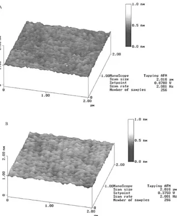
We further studied the oxidation effect on Si/Si0.6Ge0.4by mea-suring the surface roughness change using AFM. Figure 6a and b illustrate the measured surface topography before and after oxida-tion, respectively. A measured root-mean-square (rms) roughness is 1.3 and 1.6 Å for Si/Si0.6Ge0.4before and after oxidation, respec-tively. It is important to notice that these rms values are also compa-rable with thermal SiO2grown on Si substrate.20The very smooth oxide surface also suggests that the high temperature (9008C) formed Si/Si0.6Ge0.4is stable during subsequent high-temperature (9008C) oxidation. This is due to the formed Si0.6Ge0.4that is already strain-relaxed during the first high-temperature solid phase epitaxy. Furthermore, no strain relaxation related roughness reported previ-ously14could be identified in AFM figures. Therefore, the reason for good oxide quality may be ascribed to both high oxidation tempera-ture, smooth and pinhole free oxide surface. This result is in sharp contrast to traditional low-temperature chemical vapor deposition grown SiGe because strain relaxation and defect generation are observed during high-temperature oxidation.
Conclusions
We have developed a new method to grow high-quality thermal oxide on Si0.6Ge0.4with a thin Si top layer. The good oxide integri-ty is due to the high-temperature thermal oxidation directly on Si top layer, with additional strain relaxed and thermally stable Si0.6Ge0.4 formed by solid phase epitaxy at high temperatures. The advantage of this process is that it provides a simple and inexpensive way to form SiGe with high-quality gate oxide and this process is fully compatible to the current CMOS technology.
Acknowledgments
The authors greatly appreciate the contribution of Professor K. C. Hsieh of the Department of Electrical Engeering, University of Illi-nois, and C. Tsai, previously of our Department, for the fruitful com-ments and suggestions. This work has been supported by NSC (88-2215-E-009-032) of Taiwan.
National Chiao Tung University assisted in meeting the publication costs of this article.
Reference
1. W. Ting, G. Q. Lo, J. Ahn T. Y. Chu, and D. L. Kwong, IEEE Electron Device Lett.,
12, 416, (1991).
2. C. T. Liu, Y. Ma, J. Becerro, S. Nakahara, D J. Eaglesham, and S. J. Hillenius, IEEE Electron Device Lett., 18, 105, (1997).
3. M.-Y. Hao, Kafai Lai, W.-M. Chen, and J. C. Lee, Tech. Dig. Int. Electron Devices Meet., 601 (1994).
4. A. Chin, C. C. Liao, C. H. Lu, W. J. Chen, and C. Tsai, Symposium on VLSI Tech-nology, p. 135, Kyoto, Japan (1999).
5. F. K. LeGoues, R. Rosenberg, T. Nguyen, F. Himpsel, and B. S. Meyerson, J. Appl. Phys., 65, 1724, (1989).
6. H. K. Kiou, P. Mei, U. Gennser, and E. S. Yang, Appl. Phys. Lett., 59, 1200, (1991). 7. D. K. Nayak, K. Kamjoo, J. S. Park, J. C. S. Woo, and K. L. Wang, Appl. Phys.
Lett., 57, 369, (1990).
8. I. S. Goh, S. Hall, W. Eccleston, J. F. Zhang, and K. Werner, Electron Lett., 30, 1988, (1994).
9. P. W. Li, E. S. Yang, Y. F. Yang, J. O. Chu, and B. S. Meyerson, IEEE Electron Device Lett., 15, 402 (1994).
10. D. Tchikatilov, Y. F. Yang, and E. S. Yang, Appl. Phys. Lett., 69, 2578 (1996). 11. S. S. Iyer, Paul M. Solomon, V. P. Kesan, A. A. Bright, John L. Freeouf, Thao N.
Nguyen, and Alan C. Warren, IEEE Electron Device Lett., 12, 246 (1991). 12. V. P. Kesan, S. Subbanna, P. J. Restle, M. J. Tejwani, J. M. Altken, S. S. Iyer, and
J. A. Ott, Tech. Dig. Int. Electron Devices Meet., 25 (1991).
13. J. Welser, J. L. Hoyt, and J. F. Gibbons, IEEE Electron Device Lett., 15, 100 (1994). 14. S. Verdonckt-Vandebroek, E. F. Crabbe, B. S. Meyerson, D. L. Harame, P. J. Res-tle, J. M. C. Stork, and J. B. Johnson, IEEE Trans. Electron Devices, 41, 97 (1996). 15. Y. Taur and T. K. Ning, Fundamentals of Modern VLSI Devices, p. 286, Cambridge
University Press, Cambridge (1998).
16. Y. H. Wu, W. J. Chen, S. L. Chang, A. Chin, S. Gwo, and C. Tsai, IEEE Electron Device Lett., 20, 200 (1999).
17. Y. H. Wu, W. J. Chen, A. Chin, and C. Tsai, Appl. Phys. Lett., 74, 528 (1999). 18. Y. H. Wu, W. J. Chen, A. Chin, and C. Tsai, 41st Electronic Materials Conf., 1999,
Santa Barbara, CA.
19. Y. Taur and T. K. Ning, Fundamentals of Modern VLSI Devices, p. 196, Cambridge University Press, Cambridge (1998).
20. J. M. Lai, W. H. Chieng, B. C. Lin, Albert Chin, and C. Tsai, J. Electrochem. Soc.,
146, 2216 (1999). Figure 5. SILC effect of 50 Å thermal oxide grown on 30 Å Si/350 Å
Si0.6Ge0.4measured under 25 V for 10,000 s.
Figure 6. AFM surface morphology (a) before and (b) after 50 Å thermally oxide grown on 30 Å Si/350 Å Si0.6Ge0.4.
) unless CC License in place (see abstract).
ecsdl.org/site/terms_use
address. Redistribution subject to ECS terms of use (see
140.113.38.11