IEEE PHOTONICS TECHNOLOGY LETTERS, VOL. 22, NO. 4, FEBRUARY 15, 2010 257
Efficiency Improvement of GaN-Based
Light-Emitting Diode Prepared on GaN
Nanorod Template
C. H. Kuo, L. C. Chang, C. W. Kuo, and G. C. Chi
Abstract—We demonstrated the formation of GaN-based nanorod (NR) structure by using self-assemble Ni nanoislands as the etching mask. It was found that crystal quality of the GaN epilayer prepared on an NR GaN template was significantly better than that prepared with a conventional low-temperature GaN nucleation layer. With the NR GaN template, it was found that 20-mA light-emitting diode (LED) output power can be enhanced by 39.8%, as compared to the conventional LED.
Index Terms—InGaN–GaN, light-emitting diode (LED), nano, template.
I. INTRODUCTION
G
ALLIUM nitride (GaN) and its related compounds such as AlGaN and InGaN have emerged as important semi-conductor materials for high-performance light emitters in the ultraviolet (UV), blue, and green spectral regions [1], [2]. How-ever, one still needs to further improve output efficiency of these GaN-based light-emitting diodes (LEDs) for applications such as solid-state lighting. It is known that crystal quality of the GaN epitaxial layers prepared on sapphire substrate is poor due to the large mismatches in lattice constant and thermal expansion coefficient between GaN and sapphire. These mismatches will result in a large number of threading dislocations (TDs) in the epitaxial layers. This could severely degrade the performance of GaN-based LEDs. Previously, it has been shown that one can use techniques such as epitaxial lateral overgrowth (ELO) and pendeo epitaxy (PE) to overcome this problem [3], [4]. ELO is to deposit a stripe-type SiO mask, through photolithography, onto a GaN template. Lateral overgrowth can thus occur since GaN can only be grown selectively on the window regions [3]. Al-though ELO can effectively suppress TD density in the laterally overgrown mask regions, defect density in the vertically grown window regions is still high. Similar to ELO, it is also neces-sary to deposit a stripe-type SiO mask, through photolithog-raphy, onto a GaN template for PE. Prior to regrowth, however, one needs to use an inductively coupled plasma (ICP) etcher toManuscript received August 29, 2009; revised November 19, 2009; accepted December 04, 2009. First published January 12, 2010; current version published January 29, 2010. This work was supported by the National Science Council of Taiwan under Research Grant NSC 98-2221-E-008-002-MY3.
C. H. Kuo, L. C. Chang, and C. W. Kuo are with the Department of Optics and Photonics, National Central University, Jhongli, Taoyuan 32001, Taiwan (e-mail: [email protected]; [email protected]; [email protected]).
G. C. Chi is with the Department of Photonics, National Chiao Tung Univer-sity, Hsinchu, 300, Taiwan (e-mail: [email protected]).
Color versions of one or more of the figures in this letter are available online at http://ieeexplore.ieee.org.
Digital Object Identifier 10.1109/LPT.2009.2038595
etch away the exposed GaN for PE. Thus, the growth was forced to begin laterally from the etched sidewalls. Compared to ELO which only provides low TD in the mask region, PE can provide low TD density over the entire wafer [4]. It should be noted that the growth fronts over the mask regions are titled. This would result in the formation of boundaries above each mask [5]. Fur-thermore, one extra photolithography step is needed for both ELO and PE, as compared to conventional growth.
Very recently, it has been shown that one could control di-mension and density of Ni nanoislands onto a substrate uni-formly [6], [7]. It has also been shown that the self-assemble Ni nanoislands can be used as an etching hard mask. Indeed, it has been shown that natural lithography can be used to form a nanopatterned sapphire substrate [7]. In this study, we apply natural lithography to form a nanorod (NR) structure on GaN template. It will be shown that the NR structured GaN template can be used for PE without the conventional photolithography. GaN-based LEDs prepared on the NR structured GaN template were also fabricated. Electrooptical properties of the fabricated LEDs will also be discussed.
II. EXPERIMENT
The NR structure and the GaN-based LEDs used in this study were all prepared by metal–organic chemical vapor deposition (MOCVD) [8], [9]. We first deposited a low-temperature (LT) GaN nucleation layer and a 2- m-thick undoped GaN layer on a c-face sapphire substrate. A 40-nm-thick SiO film was then deposited on the GaN surface by plasma-enhanced chemical vapor deposition (PECVD), followed by deposition the 17-nm-thick Ni metal film by electron-beam evaporator. The sample was subsequently rapid thermal annealed (RTA) at 800 C for 2 min to form nanoscale Ni metal islands. The sample was then ICP etched using self-assembled Ni nanoislands as the etching hard mask. The sample was subsequently dipped in hy-drogen fluoride (HF) solution to remove the SiO after etching. Fig. 1(a) shows a scanning electron microscope (SEM) image of the etched sample. It can be seen clearly that vertical GaN NRs with an average diameter of about 250 to 500 nm were formed. It was also found that GaN NR’s density was around cm . We subsequently deposited a GaN-based LED structure on top of the NR/GaN template (i.e., NR LED). For comparison, a conventional GaN-based LED without the NR structure was also prepared (i.e., C LED). Fig. 1(b) schemati-cally depicts of the fabricated NR LED. The fabrication process of the LED can be found elsewhere [8], [9]. For comparison, conventional LED was also prepared.
258 IEEE PHOTONICS TECHNOLOGY LETTERS, VOL. 22, NO. 4, FEBRUARY 15, 2010
Fig. 1. (a) SEM images of GaN NRs template. (b) Schematic diagram of the fabricated NR LED.
Fig. 2. (a) In situ optical reflectance measured during the growth of the LED structure on NR/GaN template. The growth temperature and silane slow as a function of time was also plotted. (b) SEM images of a n-GaN surface at various GaN regrowth time on NR/GaN template. (b1) 32 min. (b2) 44 min. (b3) 60 min. (b4) 110 min. Inset in Fig. 2(b4) shows cross- sectional SEM image of the sample.
III. RESULTS ANDDISCUSSION
Previously, Koleske et al. demonstrated that transition from three-dimensional (3-D) grain to two-dimensional (2-D) coa-lesced growth can be intentionally prolonged by reducing the NH flow during the initial high-temperature GaN growth [10]. They found that such a phenomenon could be observed by in situ optical reflectance during growth. They also reported that one could reduce the TD density by prolonging the 3-D to 2-D tran-sition time. In this study, we also used the same method to char-acterize NR LED. Fig. 2(a) shows the in situ optical reflectance measured during the growth of the GaN-based LED structure on the NR/GaN template. The growth temperature as a function of time was also plotted. It can be seen clearly the 3-D to 2-D tran-sition time of this particular sample was extremely long, as com-pared to those reported previously [11], [12]. It took 110 min to reach the maximum oscillation amplitude. Fig. 2(b) shows the SEM micrographs of the n-GaN film morphology at various growth times: (b1) 32 min, (b2) 44 min, (b3) 60 min, and (b4) 110 min [indicated by an arrow in Fig. 2(a)]. During the long 3-D to 2-D transition, NRs grew and coalesced with each other. N-GaN epilayer could completely coalesce into a flat surface. Indeed, we found that surface of this sample is mirror-like after the growth, as shown in Fig. 2(b4). The inset of Fig. 2(b4) shows a cross-sectional SEM image of the GaN grown on NR/GaN template. It can be seen clearly that voids could be found at the GaN/NR interface. The electron concentration was 3.5E18 cm for the n-GaN layer on the NR/GaN template.
Fig. 3(a) and (b) shows transmission electron microscopy (TEM) images of the NR LED and conventional LED (i.e., C LED), respectively. As shown in these figures, it was found that the number of TD density observed from NR LED with the NR structure was significantly smaller than that observed from C LED without the NR structure. The much smaller TD density
Fig. 3. TEM images of the (a) NR LED and (b) C LED.
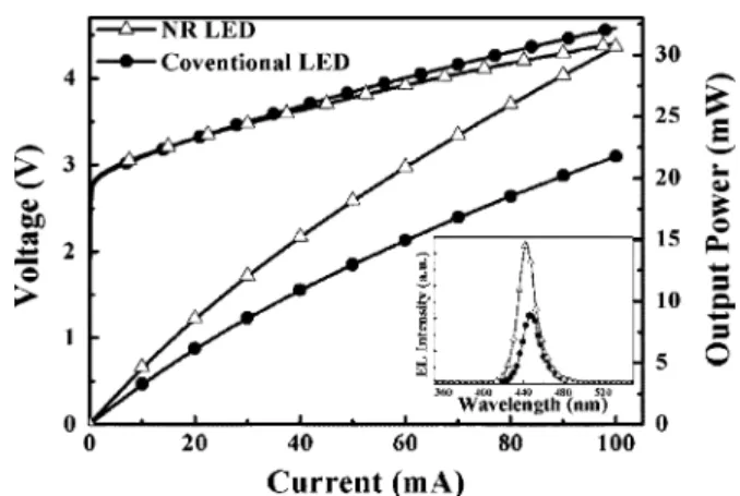
Fig. 4. L–I–V characteristics of the two fabricated LEDs. Inset shows 20-mA EL spectra of the LEDs.
observed from NR LED should be attributed to the effect of lateral growth which is similar to that reported in PE [4]. It also can be seen clearly that a number of stacking faults occurred above the voids from NR LED, where visible TDs are rarely observed in the vicinities. The void density depends on the NR’s density. Very recently, it has been shown that the presence of stacking faults could block the propagation of TDs and the bending dislocation was due to the lateral growth of GaN [13]. In other words, we could reduce the TDs with increasing the NR’s density. We also used etch pit density (EPD) to study crystal quality of these two samples by immersing them in H PO at 160 C for 3 min. It was found that EPD were around 1.9E8 and 5.1E8 cm for n-GaN on NR/GaN template and conventional n-GaN, repectively. Therefore, we could reduce the TD density by using the NR/GaN template.
The inset of Fig. 4 shows 20-mA electroluminescence (EL) spectra of the fabricated LEDs. It was found that EL peak posi-tions of these two LEDs occurred around 450 nm with the same full-width at half-maximum (FWHM) of 21 nm. This should be attributed to the same LED structure used in these two de-vices. Fig. 4 shows intensity–current–voltage ( – – ) charac-teristics of the two LEDs. It was found that series resistance measured from NR LED was lower than conventional LED. It should be noted that the regrowth layer on the NR/GaN template is n-GaN, as shown in Fig. 2(a). Thickness of the n-GaN layer of NR LED is 5.3 m. Generally, the thickness of the n-GaN layer of C LED is 3.8 m. Therefore, it could be attributed to the NR LED with good current spreading by using 5.3- m n-GaN layer, compare with C LED. With 20-mA injection current, it was also found that forward voltages were 3.30 and 3.30 V while
KUO et al.: EFFICIENCY IMPROVEMENT OF GaN-BASED LED PREPARED ON GaN NR TEMPLATE 259
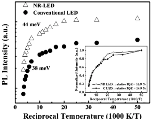
Fig. 5. Arrhenius plot of the integrated PL intensity obtained from the main emission peak over the temperature range from 20 K to 300 K of the two LEDs. The inset of Fig. 5 was relative PL quantum efficiency as a function of temper-ature.
output powers were 8.60 and 6.15 mW for the NR LED and C LED, respectively. With 20-mA injection current, it was found that we achieved a 39.8% enhancement in output power from the NR-LED, as compared to conventional LED. There are two reasons that account for the enhancement in output power from the NR-LED. First, NR-LED should be attributed to the reduced TD density and thus the reduced probability of nonradiative re-combination for the LED prepared on the NR/GaN template. Second, the higher light extraction efficiency (LEE) is related to the light scattering from the embedded air void between the GaN–sapphire interface by increasing the refractive index dif-ference [14]. The figure shown in Fig. 1(b) can be used to ex-plain such an enhancement. A reliability test of the NR-LED is underway and the results will be reported separately.
In order to further clarify the reason for the enhancement of LED output power in the NR LEDs, temperature-dependent PL measurements were performed. Fig. 5 shows Arrhenius plots of the normalized integrated PL intensity for the PL emission over the temperature range. It was found that the integrated PL intensity dropped slowly with the temperature during the low-temperature region, whereas it decreased rapidly during the high-temperature region. The best fitting gives two activation energies of about 44 and 38 meV for NR LED and C LED, re-spectively. Such an enhancement in activation energy is also the evidence that the NR-LED has lower dislocation density and higher internal quantum efficiency (IQE) [15]. The inset of Fig. 5 shows that the relative IQE was estimated by comparing the low temperature (20 K) with the RT-PL (300 K) assuming that the PL IQE at low temperature (20 K) is equal to 1 [16]. It was found that relative IQE of NR LED and C LED were 16.9% and 14.9%, respectively. The higher relative IQE of NR LED indicated that the NR LEDs have better radiative recombination efficiency, as compared to conventional LED. In other words, the IQE was enhanced by 13.4% of NR LED. Therefore, from the output power enhancement (39.8%) and the IQE enhance-ment (13.4%), we predicted that the LEE enhanceenhance-ment would be 26.4% by embedded air void between the GaN–sapphire in-terface.
IV. CONCLUSION
In summary, we report the growth mechanism of a GaN regrown NR structure and the fabrication of NR-LED. It was found that we could significantly reduce the TD density and enhance LEE using the NR structure. With the NR structure, it was found that 20-mA LED output power can be enhanced by 39.8%.
REFERENCES
[1] T. Mukai, M. Yamada, and S. Nakamura, “Characteristics of InGaN-based UV/blue/green/amber/red light-emitting diodes,” Jpn. J. Appl.
Phys., vol. 38, no. 7A, pp. 3976–3981, Jul. 1999.
[2] S. J. Chang, W. C. Lai, Y. K. Su, J. F. Chen, C. H. Liu, and U. H. Liaw, “InGaN-GaN multiquantum-well blue and green light-emitting diodes,” IEEE J. Sel. Topics Quantum Electron., vol. 8, no. 2, pp. 278–283, Mar. 2002.
[3] O. Nam, M. D. Bremser, T. S. Zheleva, and R. F. Davis, “Lateral epi-taxy of low defect density GaN layers via organometallic vapor phase epitaxy,” Appl. Phys. Lett., vol. 71, no. 18, pp. 2638–2640, Nov. 1997. [4] I. H. Kim, C. Sone, O. H. Nam, Y. J. Park, and T. Kim, “Crystal tilting in GaN grown by pendoepitaxy method on sapphire substrate,” Appl.
Phys. Lett., vol. 75, no. 26, pp. 4109–4111, Dec. 1999.
[5] A. M. Roskowski, E. A. Preble, S. Einfeldt, P. M. Miraglia, and R. F. Davis, “Maskless pendeo-epitaxial growth of GaN films,” J. Electron.
Mater., vol. 31, no. 5, pp. 421–428, 2002.
[6] H. W. Huang, J. T. Chu, T. H. Hsueh, M. C. Ou-Yang, H. C. Kuo, and S. C. Wang, “Fabrication and photoluminescence of InGaN-based nanorods fabricated by plasma etching with nanoscale nickel metal is-lands,” J. Vac. Sci. Technol. B, vol. 24, no. 4, pp. 1909–1912, 2006. [7] H. Gao, F. Yan, Y. Zhang, J. Li, Y. Zeng, and G. Wang, “Enhancement
of the light output power of InGaN/GaN light-emitting diodes grown on pyramidal patterned sapphire substrates in the micro- and nanoscale,”
J. Appl. Phys., vol. 103, p. 014314, Jan. 2008.
[8] S. J. Chang, C. H. Kuo, Y. K. Su, L. W. Wu, J. K. Sheu, T. C. Wen, W. C. Lai, J. F. Chen, and J. M. Tsai, “400-nm InGaN–GaN and InGaN–AlGaN multiquantum well light-emitting diodes,” IEEE J.
Sel. Topics Quantum Electron., vol. 8, no. 4, pp. 744–748, Jul. 2002.
[9] S. J. Chang, W. S. Chen, S. C. Shei, T. K. Ko, C. F. Shen, Y. P. Hsu, C. S. Chang, J. M. Tsai, W. C. Lai, and A. J. Lin, “Highly reliable high-brightness GaN-based flip chip LEDs,” IEEE Trans. Adv. Packag., vol. 30, no. 4, pp. 752–757, Nov. 2007.
[10] D. D. Koleske, A. J. Fischer, A. A. Allerman, C. C. Mitchell, K. C. Cross, S. R. Kurtz, J. J. Figiel, K. W. Fullmer, and W. G. Breiland, “Improved brightness of 380 nm GaN light emitting diodes through in-tentional delay of the nucleation island coalescence,” Appl. Phys. Lett., vol. 81, no. 11, pp. 1940–1942, Sep. 2002.
[11] C. H. Kuo, S. J. Chang, Y. K. Su, C. K. Wang, L. W. Wu, J. K. Sheu, T. C. Wen, J. M. Tsai, W. C. Lai, and C. C. Lin, “Nitride-based blue LEDs withGaN/SiN double buffer layers,” Solid-State Electron., vol. 47, pp. 2019–2022, 2003.
[12] S. C. Wei, Y. K. Su, S. J. Chang, S. M. Chen, and W. L. Li, “Nitride-based MQW LEDs with multiple GaN-SiN nucleation layers,” IEEE
Trans. Electron Devices, vol. 52, no. 6, pp. 1104–1109, Jun. 2005.
[13] C. H. Chiu, H. H. Yen, C. L. Chao, Z. Y. Li, P. Yu, H. C. Kuo, T. C. Lu, S. C. Wang, K. M. Lau, and S. J. Cheng, “Nanoscale epitaxial lateral overgrowth of GaN-based light-emitting diodes on a SiO nanorod-array patterned sapphire template,” Appl. Phys. Lett., vol. 93, p. 081108, Aug. 2008.
[14] E. H. Park, J. Jang, S. Gupta, I. Ferguson, C. H. Kim, S. K. Jeon, and J. S. Park, “Air-voids embedded high efficiency InGaN-light emitting diode,” Appl. Phys. Lett., vol. 93, p. 191103, Nov. 2008.
[15] Y. H. Cho, G. H. Gainer, A. J. Fischer, J. J. Song, S. Keller, U. K. Mishra, and S. P. Denbaars, ““S-shaped” temperature-dependent emission shift and carrier dynamics in InGaN/GaN multiple quantum wells,” Appl. Phys. Lett., vol. 73, no. 10, p. 1370, Sep. 1998. [16] S. Watanabe, N. Yamada, M. Nagashima, Y. Ueki, C. Sasaki, Y.
Ya-mada, T. Taguchi, K. Tadatomo, H. Okagawa, and H. Kudo, “Internal quantum efficiency of highly-efficient In Ga N-based near-ultra-violet light-emitting diodes,” Appl. Phys. Lett., vol. 83, no. 24, p. 4906, Dec. 2003.