國立交通大學
電子工程學系 電子研究所碩士班
碩士論文
多晶矽
多晶矽
多晶矽
多晶矽奈米線結合內嵌式奈米
奈米線結合內嵌式奈米
奈米線結合內嵌式奈米矽
奈米線結合內嵌式奈米
矽
矽
矽晶體之
晶體之
晶體之
晶體之
SONOS 記憶體元件之
記憶體元件之
記憶體元件之
記憶體元件之研
研
研究
研
究
究
究
A Study on Poly-Si Nanowire SONOS Devices
with In-Situ Embedded Silicon Nanocrystals
研 究 生:羅正瑋
指導教授:林鴻志 博士
黃調元 博士
多晶矽
多晶矽
多晶矽
多晶矽奈米線結合內嵌式奈米
奈米線結合內嵌式奈米
奈米線結合內嵌式奈米矽
奈米線結合內嵌式奈米
矽
矽
矽晶體之
晶體之
晶體之
晶體之
SONOS 記憶體元件之
記憶體元件之
記憶體元件之
記憶體元件之研
研
研究
研
究
究
究
A Study on Poly-Si Nanowire SONOS Devices
with In-Situ Embedded Silicon Nanocrystals
研 究 生:羅正瑋 Student: Cheng-Wei Luo 指導教授:林鴻志 博士 Advisors: Dr. Horng-Chih Lin 黃調元 博士 Dr. Tiao-Yuan Huang
國立交通大學
電子工程學系 電子研究所碩士班
碩士論文
A Thesis
Submitted to Department of Electronics Engineering & Institute of Electronics College of Electrical and Computer Engineering
National Chiao-Tung University in Partial Fulfillment of the Requirements
for the Degree of Master in
Electronic Engineering July 2010
Hsinchu, Taiwan, Republic of China
多
多
多
多晶矽
晶矽奈米線結合內嵌式奈米
晶矽
晶矽
奈米線結合內嵌式奈米
奈米線結合內嵌式奈米矽
奈米線結合內嵌式奈米
矽晶體之
矽
矽
晶體之
晶體之
晶體之
SONOS 記憶體元件之
記憶體元件之
記憶體元件之研
記憶體元件之
研
研
研究
究
究
究
研究生 研究生 研究生 研究生::::羅正瑋羅正瑋羅正瑋 指導教授羅正瑋 指導教授:指導教授指導教授:::林鴻志林鴻志林鴻志林鴻志 博士博士博士博士 黃調元黃調元黃調元 博士黃調元 博士博士博士 國立交通大學 國立交通大學國立交通大學 國立交通大學 電子工程學系 電子工程學系電子工程學系 電子工程學系 電子研究所碩士班電子研究所碩士班電子研究所碩士班 電子研究所碩士班
摘
摘
摘
摘 要
要
要
要
在本篇論文中,我們利用本實驗室最近發展出的多晶矽奈米線製程來製作 SONOS 元件,此製程無須使用先進且昂貴的設備,其製作流程簡單且極富彈性。 藉由稍微調整製程的參數,我們製作了四種不同截面尺寸的奈米線元件。相較於 平面結構元件,奈米線元件具有較好的次臨界擺幅(subthreshold swing)以及較大的開關電流比(on/off current ratio),而且奈米線元件在寫入和抹除速度上也有
很大幅度的改善。在這四種不同截面尺寸的奈米線元件中,我們的數據顯示較細 的元件擁有較快的寫入和抹除速度,但也會較快進入寫入飽和狀態。 此外,我們運用內嵌式奈米矽晶體(silicon nanocrystals)製程,將奈米矽晶 體嵌入氮化矽層間,以此來製作 SONOS 元件。利用改變奈米矽晶體在氮化矽層 內的相對位置,可以得到許多特性非常不同的元件。當奈米矽晶體位於氮化矽及 穿隧氧化層間時,元件會有最快的寫入和抹除速度。而當奈米矽晶體位鑲嵌於氮 化矽內時,元件的電荷保持能力(retention)最好。 本論文中的所有元件,在可靠度方面都擁有不錯的電荷保持能力及忍耐力 (endurance),這些元件都可以承受超過一萬次的重複寫入及抹除,並且在十年 儲存後,仍可維持大於 0.5 V 的記憶窗(memory window)。
A Study on Poly-Si Nanowire SONOS Devices
with In-Situ Embedded Silicon Nanocrystals
Student: Cheng-Wei Luo Advisors: Dr. Horng-Chih Lin Dr. Tiao-Yuan Huang
Department of Electronics Engineering and Institute of Electronics
National Chiao Tung University, Hsinchu, Taiwan
Abstract
In this thesis, we employed a simple, low cost, and flexible way that was recently developed by our group to fabricate NW devices. With a slight modification in fabrication procedure, gate-all-around NW SONOS devices with four different cross-sectional dimensions were implemented. Compared with planar control, NW devices possess higher on/off current ratio and superior SS. Moreover, NW SONOS devices have apparent improvement on P/E speed. In these four SONOS splits with different dimensions, the thinnest exhibits the best SS due to its best gate controllability. Comparing the P/E characteristics, thinner device depicts higher P/E speed but reaches the programming saturation more quickly.
We have also fabricated Si NCs devices based on the poly-Si NW SONOS technology. Accompanying with the changing of Si NCs location in the nitride trapping layer, these memory devices also exhibit very different P/E performances. Specifically, when Si NCs are located at the interface of tunneling oxide and nitride
layer, the device possesses the fastest P/E speed among all splits.On the other hand, when Si NCs are embedded in the nitride layer, the device shows the best retention performance.
For reliability test, all NW SONOS devices studied in this thesis can maintain acceptable memory window after 104 P/E cycles. The data retention measurements of these devices show that the memory window can be larger than 0.5 V after 10 years at room temperature.
Acknowledgement
畢業典禮的這天,我要在這裡感謝所有在這一路上幫助過我的人。兩年的時 間,似乎不算長,但是,幫助過我的人,卻讓我數都數不完。 首先,我要感謝我的指導教授 林鴻志 教授及 黃調元 教授。兩位老師在很 多方面都為我著想,當他們知道我有意願出國時,就開始處處幫我留心,讓我能 夠有更多更好的機會以讓我之後在申請學校上能夠更順利,並一直指引我正確的 方向,讓我從中不斷地學習並不斷累積許多寶貴的經驗。在我的一生中,能夠有 機會在兩位教授身旁學習、成長,真的是一件非常幸運的事情。 再來,我要感謝的是 631 的六位戰友,謝謝簡敏峰(真‧白 toro 假面)、林 庭輔(教材輔)、陳冠宇(NM)、劉禹伶(劉媽)、許家維、陳冠智。真‧白 toro 假面在各方面的進度上遠遠的超越實驗室裡的每一位同學,給予我極大的壓力, 讓我能夠不斷的向前。教材輔偶爾會發生一些有趣的事帶給實驗室許多話題。 NM 總是給予實驗室許多的歡樂,是實驗室裡最有活力的一位。劉媽常常為實驗 室的每位同學著想並讓實驗室維持整潔。許家維常常與我討論課業上的問題,讓 我對事物有更深的了解。另外,也要謝謝許多學長,徐行徽(徐博)學長總是帶 著我做實驗,並聽我發牢騷。陳威臣(大師)學長給予我更廣闊的思維,也與我 討論實驗的結果。林哲民(阿民)則是與我討論許多新的實驗的可能性,並激發 出更多不同的想法。蔡子儀學長則帶給實驗室許多的笑聲。林政穎(阿毛)和郭 嘉豪(馬腳)學長則像我們同屆同學一樣。感謝以上的各位,讓我的碩士生涯中 添加不少樂趣。我還要感謝我的高中同學,嚴中健及李孟寰,有時候會陪我吃吃 喝喝,聊天打屁。另外,我要謝謝大學時的同學,君凌、老涂、淳博、小瑩、小 白和江帥,有你們陪著我,讓我在剛進入交大時不會覺得寂寞,也常常在我實驗 不順時聽著我抱怨,謝謝你們。 最後,也是最重要的,我要感謝在這兩年中一直挺我的家人。有你們在,讓 我能夠毫無畏懼的向前走,有你們在,讓我在挫折中能再爬起來,有你們在,讓 我能夠分享我喜悅。謝謝你們。 羅正瑋 2010.06.26Contents
Abstract (Chinese)……….. I Abstract (English)………... II
Acknowledge……… IV Contents ……….. V
Table Captions.………...………. VIII Figure Captions ……….. IX
Chapter 1 Introduction………... 1
1.1 Overview of Multiple-Gated Structure and Nanowire Technology………...……. 1
1.2 Overview of SONOS Flash Memory………...……….... 3
1.3 Introduction of Nanocrystal Nonvolatile Memory………. 4
1.4 Motivation ……….. 6
1.5 Organization of the Thesis ………. 6
Chapter 2 Device Fabrication……… 7
2.1 Intructure and Fabrication of Nanowire SONOS Devices……….. 7
2.2 Structure and Fabrication of Planar SONOS Devices………... 10
2.3 In-Situ Embedded Silicon Nanocrystals………... 10
2.4 The Measurement Setup……….. 12
2.5 Program/Erase Mechanisms of SONOS Flash Memory………. 12
2.5.1 Fowler-Nordheim (FN) Tunneling………. 13
2.5.3 Channel Hot Electrons Injection……….... 14
2.5.4 Band-to-Band Tunneling……… 15
2.5.5 Program/Erase Operation Principles……….. 16
2.6 Reliability of SONOS Flash Memory………. 16
2.6.1 Retention……… 16
2.6.2 Endurance……….. 17
Chapter 3 Characteristics of Planar and Nanowire SONOS Devices with Various Dimensions………. 19
3.1 Basic Transfer Characteristics of Planar and NW SONOS………. 19
3.2 Program/Erase Characteristics………... ……… 20
3.2.1 Program/Erase Characteristics of Planar and NW SONOS………. 21
3.2.2 Program Characteristics of NW SONOS... ………. 22
3.2.3 Erase Characteristics of NW SONOS……….. 24
3.3 Reliability Characteristics of Planar and NW SONOS………... 24
3.3.1 Endurance……. ………...………... 24
3.3.2 Retention………….. ………... 25
Chapter 4 Characteristics of SONOS Devices with In-Situ Embedded Silicon Nanocrystals………... 26
4.1 Basic Transfer Characteristics………. 26
4.2 Program/Erase Characteristics………... 27
4.2.1 Program Characteristics of STD and Si NCs NW SONOS………. 27
4.2.2 Erase Characteristics of STD and Si NCs NW SONOS……….. 29
4.3.1 Endurance………...………. 32
4.3.2 Retention……….. 32
Chapter 5 Conclusions and Future Work………... 34
5.1 Conclusions…………... 34 5.2 Future Work…………... 35 References………... 37 Figures………. 42 Vita………... 84 Publish List……….. 85
Table Captions
Chapter 5
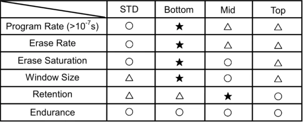
Table I Conditions of these four different dimensions NW SONOS………. 18 Table II Comparison between STD and Si NCs devices. ★ Excellent
○
GoodFigure Captions
Chapter 2
Fig. 2-1 (a) Layout and (b) cross-sectional view of NW SONOS………... 42
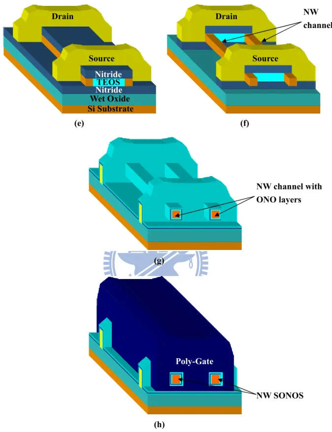
Fig. 2-2 Process flow of NW SONOS memory device. (a) Deposition of hard mask/TEOS oxide/bottom nitride layers. (b) Patterning of hard mask and TEOS oxide by anisotropic etching. (c) DHF lateral etching. (d) a-Si deposition and SPC. (e) Definition of S/D. (f) Removal of TEOS and nitride by wet etching. (g) Deposition of ONO layers. (h) Poly gate deposition..………. 43
Fig. 2-3 Cross-sectional TEM image of an NW SONOS memory device………….. 44
Fig. 2-4 Cross-sectional TEM image of S1 and S4………. 44
Fig. 2-5 The layout of planar SONOS memory device..………. 45
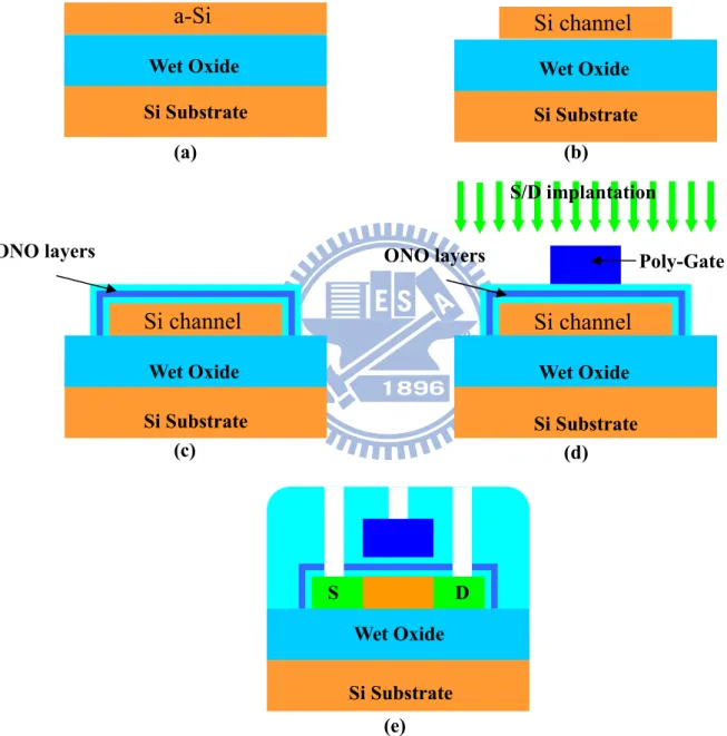
Fig. 2-6 Process flow of planar SONOS memory device. (a) a-Si layer deposition and SPC. (b) Definition of S/D and channel. (c) Deposition of ONO layers. (d) Poly gate deposition and definition, S/D implantation. (a) Passivation layer deposition and contact holes opening..……….. 45
Fig. 2-7 (a) Position and (b) change of gas flow of Bottom Si NCs……… 46
Fig. 2-8 (a) Position and (b) change of gas flow of Mid Si NCs………. 46
Fig. 2-9 (a) Position and (b) change of gas flow of Top Si NCs………. 46
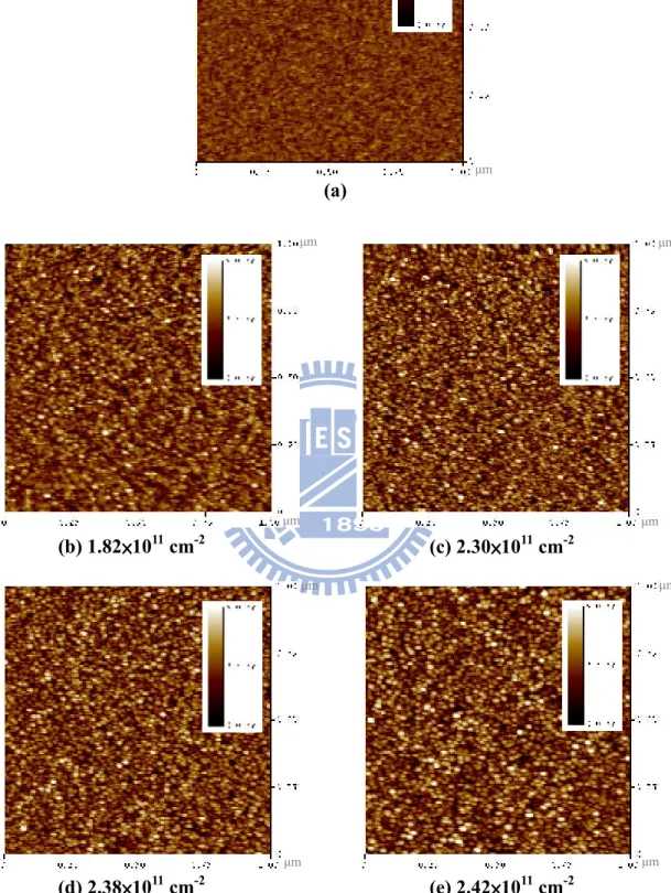
Fig. 2-10 1 ×1 µm2 AFM image of Si NCs formed on nitride film with different SiH2Cl2 deposition time of (a) 0s. (b) 20s. (c) 30s. (d) 45s. (e) 60s……….. 47
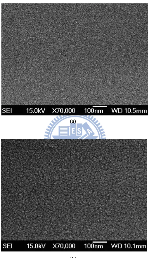
Fig. 2-11 SEM image of the nitride film (a) without and (b) with Si NCs for a deposition time of 45 seconds..……….. 48
Fig. 2-13 Cross-sectional TEM image of mid Si NCs device………... 49 Fig. 2-14 Energy band diagrams of electron injection from Si-sub to nitride under
various biases. (a) Fowler-Nordheim (FN) tunneling. (b) Direct tunneling. Φ1 is the tunneling oxide barrier height for electron. Φ2 is the conduction
band-offset between nitride and oxide..………. 50 Fig. 2-15 Channel hot electrons caused by strong lateral electrical field in pinch-off
region..………... 50 Fig. 2-16 Band-to-Band Tunneling (BTBT). (a) Deep depletion appears in n+ drain
region overlapped by gate. (b) Main tunneling mechanism occurs in deep depletion
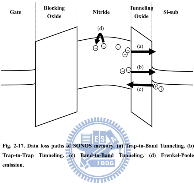
region..………... 51 Fig. 2-17 Data loss paths of SONOS memory. (a) Trap-to-Band Tunneling. (b)
Trap-to-Trap Tunneling. (c) Band-to-Band Tunneling. (d) Frenkel-Poole emission.……….………... 52
Chapter 3
Fig. 3-1 Transfer characteristics of planar and NW devices with channel lengths of 1 µm (a) before (b) after being normalized to channel width.………….….. 53 Fig. 3-2 Transfer characteristics of NW devices with different channel lengths. (a)
S1 (b) S2 (b) S3 (c) S4 splits.……….… 55 Fig. 3-3 Statistical analysis of mean values of SS for NW devices of different
dimensions. Error bars represent standard deviations.………... 56 Fig. 3-4 ID-VG characteristics of a NW SONOS device before and after
programming operation……….. 56 Fig. 3-5 (a) Programming characteristics of planar and NW SONOS devices. (b) 57
Erasing characteristics of planar and NW SONOS devices………... Fig. 3-6 Band diagrams for planar (solid) and GAA NW (dashed) devices under (a)
programming and (b) erasing operations………... 58 Fig. 3-7 Program characteristics of (a) S1, (b) S2, (c) S3, and (d) S4 splits of NW
devices with channel lengths of 0.4 µm………. 60 Fig. 3-8 Program characteristics of NW devices of S1, S2, S3 and S4 splits. The
stressing time of 100µs is used as a demarcation to divide this curve into Region I and Region II………... 61 Fig. 3-9 Band diagrams for NW devices with two different dimensions under
programming operation of Region (a) I and (b) II………. 62 Fig. 3-10 Program characteristics of NW devices of S1, S2, S3 and S4 splits……….. 63 Fig. 3-11 Erase characteristics of NW devices of (a) S1, (b) S2, (c) S3, and (d) S4
splits with channel lengths of 0.4 µm……… 65 Fig. 3-12 Erase characteristics of NW devices of S1, S2, S3 and S4 splits………….. 66 Fig. 3-13 Band diagrams for NW devices with large and small dimensions under
erasing operations………...………... 66 Fig. 3-14 Endurance characteristics of (a) S1, (b) S2, (c) S3, and (d) S4 NW devices
with channel lengths of 0.4 µm……….. 68 Fig. 3-15 ID-VG characteristics of NW SONOS device before and after 104 P/E
cycles……….. 69 Fig. 3-16 Retention characteristics of S1, S2, S3 and S4 NW SONOS device with
channel lengths of 0.4 µm at room temperature………. 69
Chapter 4
channel length of 0.4 µm. ...….……….. 70 Fig. 4-2 Program characteristics of (a) STD, (b) Bottom Si NCs, (c) Mid Si NCs
and (d) Top Si NCs splits of NW devices with channel length of 0.4 µm…. 72 Fig. 4-3 Program characteristics of STD and bottom Si NCs devices with the
program voltages of 9 V, 11 V and 13 V……… 73 Fig. 4-4 Band diagrams of STD and bottom Si NCs devices under the same
program voltages. ……….. 73 Fig. 4-5 Mean location of trapped electrons versus programming time [46]. The
Box and Tox denote the tunneling oxide and the blocking oxide,
respectively. ……….. 74
Fig. 4-6 Program characteristics of STD and mid Si NCs devices with program voltages of 9 V, 11 V and 13 V. ………. 75 Fig. 4-7 Program characteristics of STD and top Si NCs devices with program
voltages of 9 V, 11 V and 13 V……….. 76 Fig. 4-8 Band diagrams of STD and top Si NCs devices with the same program
voltages. ……… 76 Fig. 4-9 Erase characteristics of (a) STD, (b) Bottom Si NCs, (c) Mid Si NCs and
(d) Top Si NCs splits of NW devices with channel length of 0.4 µm……… 78 Fig. 4-10 Erase characteristics of STD and bottom Si NCs devices with gate
voltages of -9 V, -11 V and -13 V. ………. 79 Fig. 4-11 Erase characteristics of mid Si NCs device with the gate voltage of -9 V.
The erasing time of 100 µs is used as a demarcation of Stage I and II…….. 79 Fig. 4-12 Band diagrams of programmed mid Si NCs device (a) when gate bias is
zero and under the erasing operation of Stage (b) I and (c) II. ………. 80 Fig. 4-13 Erase characteristics of STD and bottom Si NCs devices with gate
Fig. 4-14 Erase characteristics of STD and top Si NCs devices with erase voltages of -9 V, -11 V and -13 V. ……… 81 Fig. 4-15 Band diagram of top Si NCs device under the (a) erasing process and (b)
erase saturation with gate bias of -13 V. ………... 82 Fig. 4-16 Endurance characteristics for STD and Si NC devices. The memory
window is initially set at about 2 V……… 83 Fig. 4-17 Data retention characteristics for STD and Si NC devices. The memory
Chapter 1
Introduction
1.1 Overview of Multiple-Gated Structure and Nanowire
Technology
The semiconductor industry has grown explosively in the past decades. The state-of-the-art technology node is at 32 nm and rapidly moving toward 25 nm. Accompanying the shrinkage of gate dimension, the lateral electric field penetration from drain to source has affected the potential distribution inside the channel significantly, known as short channel effect (SCE), such as drain-induced barrier lowering (DIBL) and threshold voltage (Vth) roll-off. SCE has become a major challenge of gate length and device pitch scaling.
To suppress SCE, multiple-gated (MG) configurations, such as double-gated FinFET [1], tri-gated [2], Ω-gated [3], nanowire (NW) [4-5], and gate-all-around (GAA) [6-8], had been reported for the fabrication of MOSFETs. Compared with conventional planar devices, the channel potential of these devices is controlled by the MG structure more effectively, resulting in much better gate control ability. Among these configurations, GAA MOSFET is the most ideal MG structure, which provides the best channel electrostatic control [6-9] due to its fully surrounding gate. The reduction in channel thickness can further improve the effectiveness of the gate control. Therefore, the GAA cylindrical NW-FET has been considered to be a potential candidate for the advanced CMOS technology.
Nanowire (NW), a stripe structure with its diameter or feature size smaller than 100nm, has been attracted a lot of attention. Since NW has a large surface-to-volume ratio and the surface condition of NW will strongly influence the carrier transport in NW, the NW can be applied in different areas from electronics [4-5], optoelectronics [10], to biological and chemical sensors [11-12]. NW structure also has other advantages which are desirable for memory devices, like high programming and erasing efficiency [13] and low voltage operation.
The approaches of fabricating NWs are typically classified into the following two categories: “top-down” and “bottom-up” [14-16]. In the top-down method, advanced lithography tools and expensive materials are usually required to form functional devices. Thus, this method has equipment limitation and flexibility issue in selecting the NW materials. Nevertheless, the top-down method has the capability of good reproducibility and precise positioning, which is suitable for mass production. The bottom-up method, which usually employs the vapor-liquid-solid (VLS) [17] to grow NWs, is more flexible for experimental purpose and cheaper than top-down method. VLS includes three stages: metal alloying, crystal nucleation, and axial growth to form NW. Nonetheless, the bottom-up method still possesses many problems, such as the difficulty to precise position and significant fluctuation in device characteristics, etc. In order to avoid the drawbacks of top-down and bottom-up methods, we recently developed a simple and low-cost method to fabricate the GAA NWs. There is no need for any advanced and costly equipment to form NWs patterns in our approach. Moreover, this method is free from metal contamination which may occur in metal-catalytic-grown NWs.
1.2 Overview of SONOS Flash Memory
Accompanying the popularization of electronic portable equipments (e.g., MP3, iPod, digital camera, etc.) and personal notebook, the demand of non-volatile memory (NVM) has increased dramatically. The rapidly growing market has brought about competitive development of flash memory technologies. Due to the feature that the stored data can retain in the flash memory even if the power is switched off, it is ideally suitable for portable electronic products. Since 1990s, floating-gate (FG) device has become the major product in NVM. However, the strong capacitive coupling of the FG to the neighboring cells and stress-induced leakage current (SILC) occurring in the tunneling oxide make conventional floating-gate non-volatile memories face serious limitations beyond 40 nm-node technology. The development of a feasible technology to replace the FG flash memory becomes necessary and urgent.
Among miscellaneous techniques, silicon-oxide-nitride-oxide-silicon (SONOS) has been considered as a potential candidate for next-generation NVM due to its numerous advantages over conventional FG memory, like higher scaling ability, multi-bit operation, and no FG coupling effect [18-20]. Contrary to FG flash memory, the carriers are stored in the discrete traps of the nitride in the SONOS cell, thus the tunneling oxide can be further scaled down without pinhole effect. If the tunneling oxide can be reduced, lower operation voltage and/or higher program/erase (P/E) speed can be achieved. Moreover, SONOS skips the coupling effect and SILC, which is pertaining to the FG flash memory, due to the replacement of the FG with a thin nitride layer and the localized nature of the charge-traps in nitride. By utilizing the discrete traps of the nitride, two-bit-per-cell operation is feasible [21], which could effectively double the density of storage data.
However, the endurance and data retention are the two major reliability issues for the SONOS cell. Recently, various approaches had been proposed for the improvement of the device performance of SONOS, like replacing the ONO layers with different materials, band-gap engineered SONOS (BE-SONOS) [22], trap layer engineered (TLE) [23], changing the doping type of gate silicon, etc. By replacing the blocking oxide layer with Al2O3 and using the TaN metal gate [24], the backward
Fowler-Nordheim (FN) tunneling was significantly suppressed and the P/E speed was also improved. The BE-SONOS was proposed to provide high erase speed and excellent data retention by replacing the traditional tunneling oxide with a composite ONO tunneling barrier. To prevent the FN tunneling of electrons from the gate into the nitride layer during erase, Resisinger et al. [25] proposed a SONOS structure with a p+ doped gate in lieu of the conventional n+ gate.
Today, polycrystalline silicon thin-film transistor (poly-Si TFT) SONOS has recently attracted much attention for the purpose of system-on-chip (SOC) or system-on-panel (SOP) integration [26] due to its full process compatibility. However, low memory speed and poor subthreshold property still are the limitations of the TFT SONOS. Based on our previous study, the poly-Si TFT with MG architectures would have better gate control ability and higher P/E efficiency. Thus, poly-Si TFT combined with SONOS and fin-like poly-Si channel [27] or nanowire channel [28] devices had been proposed. In this work, a modified process has been developed to fabricate GAA NW SONOS devices, and details of the process flow will be described in Chapter 2.
1.3 Introduction of Nanocrystal Nonvolatile Memory
in the early 1990s [29]. Silicon nanocrystals (NC) memory devices have attracted much attention recently due to their better data retention and endurance over the FG flash memory. The formation of Si NCs by high temperature annealing of substoichiometric SiOx [30] or Si-implanted SiO2 [31] layers has been reported. The
annealing temperature which is higher than 1000℃ adds a significant thermal budget to the process. Another technique, using thermal oxidation of a thin silicon layer has also been proposed [32]. To obtain an adequate charge-trap density, accurate control of the oxidation time is essential. Besides, the tunneling oxide thickness may be affected in the additional oxidation step. The aerosol deposition [33] method, which has high Si NCs density, needs special growth equipment. In the numerous techniques of forming the Si NCs, chemical vapor deposition (CVD) method has been widely used [34] due to its simple equipment usage and operation. Except Si NCs, Ge, metal, metal oxide and high-κ dielectric NCs also had been proposed for the nonvolatile memory device.
On the purpose of improving the performance of conventional SONOS flash memory, Y. J. Ahn et al [35] proposed the trap layer engineered structure which combines with nitride layer and WN nano-dot. One year later, SONOS with embedded Si NCs [23] had also been proved for its higher memory speed and larger operation window. After depositing the nitride, Si NCs were formed using silane as the gas source in low pressure chemical vapor deposition (LPCVD). Another way to fabricate embedded Si NCs SONOS memory was proposed by T. Y. Chiang [36], which simplified the fabrication process of forming Si NCs by changing the gas sources.
1.4 Motivation of This Study
Higher P/E speed, larger memory window and lower operation voltages make SONOS an attractive candidate for next-generation flash memory application. As aforementioned, GAA NW architecture exhibits better SONOS performance. In this thesis, we want to verify the influence of NW dimension on the SONOS characteristics. Furthermore, the data retention still is a major problem for SONOS memory. Even through nanocrystal-based NVM has better data retention, scaling issue and nanocrystals density still are the major problems of nanocrystal-based NVM. In this study, the Si NCs are embedded in the nitride layer to combine the advantages of the SONOS and nanocrystal-based approaches. To explore the effect of trap locations, the NCs are placed not just restricted in the middle of nitride layer, but also in the interface of the tunneling oxide/nitride layer or in the interface of nitride layer/blocking oxide. By using these three types of Si NCs NW SONOS device, we can see the very different P/E characteristics that affect by Si NCs and know which structure has more improvement in performance.
1.5 Organization of the Thesis
There are five chapters in this thesis. The overviews of nanowire technology, SONOS and nanocrystal NVM are presented in this chapter. The fabrication of NW-SONOS memory devices with embedded silicon nanocrystal are described in detail in Chapter 2. The measured data, such as P/E speed and reliability characteristics, are presented and discussed in Chapter 3. In Chapter 4, operation mechanisms about SONOS and comparisons regarding with/without embedded silicon nanocrystal devices are presented. Finally, we summarize the conclusions, and future works are suggested in Chapter 5.
Chapter 2
Device Fabrication
Two types of devices were fabricated and studied in this thesis. The first one is poly-Si NW SONOS memory. The other is planar thin-film transistor (TFT) SONOS memory. We compared the characteristics of SONOS from different channel structures. Differing from the bottom-up and top-down approaches, we employed the simple and low cost method recently developed by our group to fabricate NW devices [37-39]. Besides, we also adopted two different SONOS formation techniques, i.e., with and without embedded silicon nanocrystals (Si NCs), and studied their impacts on the devices. Furthermore, the positions of Si NCs were split into three parts, i.e., in the medium of nitride or at the interface of nitride and oxide. The detail of these process procedures are described in this chapter. Finally, we also briefly introduced some important mechanisms of SONOS memory operation, including P/E speed, data retention and endurance.
2.1 Structure and Fabrication of Nanowire SONOS Devices
Figure 2-1(a) shows the top view of the NW SONOS memory device. The dashed lines in the block of gate are the positions of NWs, which are located at the left and right sides of the gate, respectively. Fig. 2-1(b) shows the cross-sectional view along line AB in Fig.2-1(a) and the definition of NW channels thickness and width. It can be seen that the two rectangular-shaped poly-Si NW channels are embedded in the gate electrode.
Fabrication flow of the NW SONOS is illustrated in Fig. 2-2(a) ~ (h). The process of all devices in this work began on 6-inch wafers capped with a 250 nm silicon dioxide. First, an 80 nm bottom nitride layer was deposited by low pressure chemical vapor deposition (LPVCD). Next a 50 nm TEOS and 30 nm nitride (hard mask layer) were stacked sequentially as shown in Fig. 2-2(a). Then, the hard mask and TEOS oxide layers were patterned by anisotropic reactive plasma etching [Fig. 2-2(b)]. Note that the etching time should be carefully controlled because of low selectivity between nitride and TEOS. In the subsequent step, diluted HF (DHF) solution was used for lateral etching of TEOS oxide because of its high selectivity to nitride. Rectangular-shaped cavities were formed at the two sides of these patterns [Fig. 2-2(c)]. The dimension of cavities, which affects the size of NW, depends on the time of the TEOS lateral etching step and the thickness of TEOS oxide layer. Briefly, the thicker the TEOS oxide film or the longer the lateral etching time, the larger the cavities. Excellent filling capacity is a well-known feature of LPCVD process. By utilizing this merit of LPCVD, a 100 nm undoped amorphous silicon (a-Si) was deposited and the cavities formed in last step could be completely refilled by a-Si. To transform the a-Si into polycrystalline phase, solid phase crystallization (SPC) process was performed at 600 ℃ in N2 ambient for 24 hours [Fig. 2-2(d)]. Next, source and
drain (S/D) implant was carried out by P+ implantation with a dose of 5×1015 cm-2 and an energy of 25 keV. Since the process temperature of gate dielectric and poly-Si film depositions were higher than 700 ℃ and the time was sufficient for dopant activation, no additional S/D dopant activation step was necessary. Subsequently, the S/D photoresist patterns were defined by standard I-line lithography step, followed by an anisotropic plasma etching step to remove poly-Si not protected by the hard mask. The over-etching time in this step was prolonged to completely clean the sidewall,
which might otherwise affect the nanowire formation in the subsequent step. Protecting by the hard mask film in the dry etching step, poly-Si that filled the previously-existing cavities would be left intact and the NW channels were formed simultaneously [Fig. 2-2(e)]. To achieve the gate-all-around (GAA) structure, NWs must be suspended in the midair before the deposition of gate dielectric layers. Therefore, the bottom nitride, TEOS and hard mask should be removed entirely. The remaining nitride hard mask was etched by H3PO4 after the poly-Si etching. By
continuously removing the TEOS and bottom nitride layers by DHF and H3PO4, NWs
were hanged in the air [Fig. 2-2(f)]. To fabricate SONOS memory, oxide-nitride-oxide (ONO) stack was used as gate dielectric. For the standard SONOS device, the three layers in the ONO stack were deposited sequentially consisting of a 3 nm TEOS as the tunneling oxide, 8 nm nitride as the trapping layer and a 11 nm TEOS as the blocking layer [Fig 2-2(g)]. For the SONOS memory with embedded Si NCs, the trapping layer was composed of nitride and Si-NCs and the process will be described in Section 2.3. Afterwards, a 150 nm in-situ-doped n+ poly-Si was deposited and patterned as the gate electrode [Fig. 2-2(h)]. Finally, all devices were capped with a 350 nm TEOS as a passivation layer. Contact holes and test pads were formed with a standard metallization scheme.
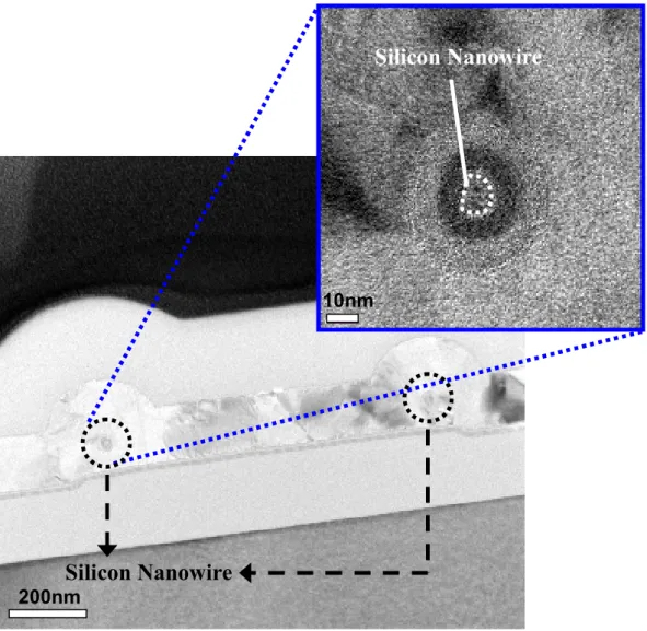
Figure 2-3 displays the TEM image of an NW SONOS memory device along line AB is illustrated in Fig 2-1(a). The sizes of channel height and thickness are approximately 15 nm. According to the color contrast in the gate dielectric, the ONO layer can be recognized clearly and the dark region corresponds to the nitride layer. In this study, we fabricate four different dimensions NW SONOS names S1, S2, S3 and S4 and list their conditions in Table I. S1 and S4 are the thickest and thinnest, respectively, and their TEM images are shown in Fig. 2-4.
2.2 Structure and Fabrication of Planar SONOS Devices
Planar SONOS devices were fabricated and characterized for comparison with the NW SONOS devices in this study. Figure 2-5 shows the top view of the NW SONOS memory device. The fabrication flow was similar to that of conventional TFTs and would be described here. First, the process started with bare silicon substrate capped with a 250 nm wet oxide layer. A 100 nm undoped a-Si film was then deposited and annealed at 600 ℃ in N2 ambient for 24 hours to transform the
a-Si into poly-Si [Fig. 2-6(a)]. Subsequently, the channel and S/D photoresist patterns were defined by a standard I-line lithography step. Next an anisotropic plasma etching was performed to remove poly-Si not protected by photoresist [Fig. 2-6(b)]. Afterwards, the gate dielectric consisting of an ONO stack of 3/8/11 nm was deposited for the standard SONOS devices [Fig. 2-6(c)]. While the process of SONOS memory with embedded Si NCs in the nitride layer will be described in Section 2.3. Next, the gate electrode formation and self-aligned S/D implant with a dose of 5×1015 cm-2 and an energy of 20 keV were carried out [Fig. 2-6(d)]. Finally, all devices were passivated with a 350 nm TEOS layer and the formation of contact holes was similar to the NW devices [Fig 2-6(e)]. There is no need for another annealing step because the process temperature of passivation layer deposition was high enough and the time was sufficiently long for dopant activation.
2.3 In-Situ Embedded Silicon Nanocrystals
In this study, the in-situ embedded Si NCs structures were split into three groups based on the locations of Si NCs. For the first split, denoted as the bottom Si NCs, the Si NCs were located at the interface of tunneling oxide and nitride layer [Fig. 2-7(a)].
The second split was denoted as the mid Si NCs, in which the Si NCs were embedded in the nitride layer [Fig. 2-8(a)]. The split with the location of Si NCs situated between the nitride and blocking oxide was denoted as the top Si NCs [Fig. 2-9(a)]. In the next paragraph, we will precisely describe the recipe of mid Si NCs, which is the most complex process among the three splits.
As shown in Fig 2-8(b), the mid Si NCs process includes three steps including bottom nitride, Si NCs and the top nitride. In the first step, LPCVD system was performed to deposit the 4 nm-thick bottom nitride film by using dichlorosilane (SiCl2H2 65-sccm) and ammonia (NH3 15-sccm) gases at 780 ℃. After the deposition
of bottom nitride, Si NCs were formed in the same tube and at the same temperature. By turning off the NH3 gas and increasing the flow rate of the SiCl2H2 to 100sccm,
the Si NCs were in-situ deposited on the wafers. SiCl2H2 was a common gas source
for the silicon layer deposition. Before the silicon film formation, silicon would nucleate and formed the Si NCs. Finally, by turning on the NH3 gas again, a 4 nm top
nitride was capped on the Si NCs in the same tube. The change of gas flow rate of SiCl2H2 and NH3 during the mid Si NCs process is illustrated in Fig. 2-8(b). Figure
2-7(b) and Fig. 2-9(b) show the steps of bottom Si NCs and top Si NCs, respectively. The density and size of Si NCs will depend on the deposition time of SiCl2H2. To
verify the effects of the deposition time, we used the atomic force microscope (AFM) to examine the Si NCs on nitride. Figure 2-10 shows the AFM surface morphologies of Si NCs on nitride with four deposition conditions. Figure 2-10(a) is the bare nitride without Si NCs, which serves as the control sample. The four conditions differed in the SiCl2H2 deposition time, i.e., 20, 30, 45 and 60 seconds, respectively. The white
spots are the relative higher point in the film. Figure 2-11 displays the top view of scanning electron microscopy (SEM) image of the nitride film without and with Si
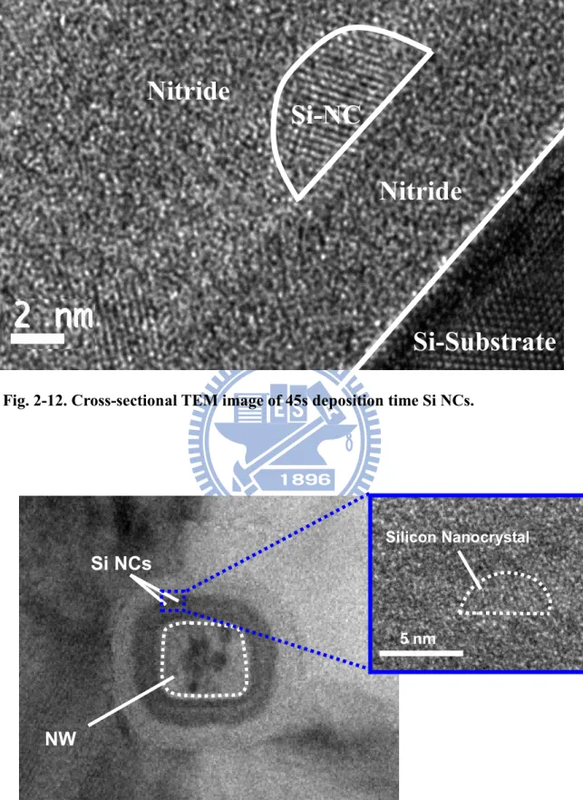
NCs for a deposition time of 45 seconds. It is obviously that with Si NCs, the surface becomes more roughness than the nitride film. Figure 2-12 is the cross-sectional TEM image of Si NCs. The crystal structure is embedded in the nitride layer. Figure 2-13. depicts the TEM image of mid Si NCs device. The dark region in ONO is the nitride layer and some lighter dots are embedded in nitride which correspond to the Si NCs.
2.4 The Measurement Setup
The experimental setup for the measurement of I-V characteristics consists of a semiconductor parameter analyzer-HP4156, a pulse generator Agilent-81110A, low leakage switch mainframe Agilent-E5250A and a Visual Engineering Environment (VEE). These equipments are controlled by the interactive characterization software (ICS) program. An exsiccator and a temperature regulator heater are used to keep the humidity and temperature at the same level.
The HP-4156 provides a high current resolution to pico-ampere range for the current measurement. The Agilent-81110A with high timing resolution generates the pulse for transient and P/E characteristics. The Agilent-E5250A switches the signal from the HP-4156 and the Agilent-81110A to the device automatically.
2.5 Program/Erase Mechanisms of SONOS Flash Memory
The basic mechanism behind the program and erase operations of SONOS is the charges transport through the tunnel dielectric. There are many charge transport mechanisms that can explain the operation behaviors of SONOS. In the following we will discuss these mechanisms of SONOS, including Fowler-Nordheim (FN) tunneling, direct tunneling, channel hot electron injection, and band-to-band tunneling.
2.5.1 Fowler-Nordheim (FN) Tunneling
FN tunneling [40] is a charge transport mechanism which depends on the gate stack composition and the applied voltage. The energy band diagram of electron injection from Si substrate to nitride under FN tunneling is illustrated in Fig. 2-14(a), in which Φ1 is the tunneling oxide barrier height for electron. FN tunneling occurs
when an electric field Eox in the oxide
ox ox
t
E ≥ Φ1 , (Eq. 2-1)
where tox is the thickness of the oxide. The electrons may tunnel through a triangular
energy barrier with a width dependent on the applied bias. The FN current density through the oxide can be describe as
− = ox c ox E E E J
α
2 exp , (Eq. 2-2) with 1 2 3 0 1 16 Φ = q q m m oxπ
hα
, (Eq. 2-3) and q q m Ec ox h 3 ) ( 2 4 2 3 1 Φ = , (Eq. 2-4)where q is the electron charge, h is the reduced Planck’s constant, m0 is the mass of
free electron and mox is the effective mass of an electron in the oxide. Eq. 2-1 is the
simplest formation of FN tunneling which doesn’t take into account the influence of temperature and image force barrier lowering.
According to the aforementioned equations, the FN tunneling current is affected by the Eox rather than the thickness of the oxide. With the same Eox, the FN current
2.5.2 Direct Tunneling (DT)
Direct tunneling (DT) [41] occurs when the Eox reduces to
ox ox ox t E t 1 2 1 −Φ < < Φ Φ . (Eq. 2-5)
The corresponding energy band diagram is shown in Fig. 2-14(b). Φ2 is the
conduction band-offset between nitride and oxide. In this condition, electrons see a trapezoidal energy barrier when they are tunneling through the oxide from the Si conduction band into the conduction band of nitride directly. The barrier width is the oxide thickness. The current density of DT can be written as
− = ox c ox E E E J
α
2 exp (Eq. 2-6) with 2 1 1 2 3 0 ) ( 1 16 ox ox ox q q qE t q m m − Φ − Φ = hπ
α
(Eq. 2-7) and q t qE q q m E ox ox ox c h 3 ) ( ) ( 2 4 2 3 1 2 3 1 − Φ − Φ = . (Eq. 2-8)Contrary to FN tunneling, the thickness of oxide affects the DT current more significantly. For an ultra thin oxide ( tox < 25 Å ), the DT is the dominant mechanism
of carrier transport. Due to retention and reliability issues, ultra thin oxide is not suitable for floating-gate type flash memory applications.
2.5.3 Channel Hot Electrons Injection
Non-uniform injection has been proposed to operate the SONOS memory. Since it has discrete traps in the trapping layer, two-bit-per-cell operation is allowed by
using non-uniform injection. Channel hot electrons injection (CHEI) [42] has been widely used for non-volatile memory application. Figure 2-15 depicts the CHEI phenomenon for NMOS. While the transistor is biased under sufficiently high gate voltage (VG) and drain voltage (VD) and VD≧VDSAT = VG – Vth, pinch-off occurs
close to drain region. The major voltage drop along the channel takes place in the pinch-off region and induces a large lateral electric field wherein. In this region, minority carriers are accelerated and gain a lot of energy, which are known as hot electrons. These hot electrons cause impact ionization and generate majority and minority carriers. The majority carriers are mostly collected and form the substrate current. The minority carriers drift into drain and contribute to drain current. Under a vertical oxide field, a fraction of highly energetic electrons would overcome the potential barrier and inject into the gate dielectric, which is so-called hot carrier injection gate current. These injected electrons will be locally trapped into the nitride layer near the drain side in SONOS memory.
2.5.4 Band-to-Band Tunneling
The mechanism of BTBT is illustrated in Fig. 2-16, which occurs in the overlap region of gate and n+ drain region. When a positive bias is applied to the drain and a highly negative gate bias will induced a deep depletion region in the n+ area next to the interface of oxide and silicon. Serious band bending in the deep depletion region will promote electrons to tunnel from valance band into conduction band. Simultaneously, holes will be left in the valence band. Portion of these holes may gain enough energy to overcome the oxide barrier and inject into gate oxide, contributing to the gate leakage current. In SONOS memory, these hot holes will inject into the nitride trapping layer and recombine with the electrons.
2.5.5 Program/Erase Operation Principles
For P/E operation in flash memory devices, there are several approaches just as mentioned in previous sections. Since the channel of our device is formed with poly-Si, grain boundaries may scatter electrons when they are transporting in the channel. Therefore, these electrons are difficult to gain sufficient energy to become hot electrons. For this reason, CHEI is not a suitable method for programming operation in our device. In this study, FN tunneling is employed for P/E operation in the poly-Si NW SONOS devices. For programming operation, both source and drain are grounded and a positive voltage is applied to the gate to induce a large electric field across the gate dielectric. Electrons in the channel will tunnel through the thin tunneling oxide and captured by the traps in the nitride layer. For erasing operation, both source and drain are grounded and a negative voltage is applied to the gate. High electric field causes some holes to inject into nitride or the trapped electrons to de-trap to the channel.
2.6 Reliability of SONOS Flash Memory
Reliability of the nonvolatile flash memory is a crucial issue for practical application. In the following, we will briefly introduce the two important topics of reliability, namely, data retention and endurance.
2.6.1 Retention
Data retention refers to the ability to keep the storage charges in the trapping layer and provide enough difference of logic level that can be distinguished. A memory window larger than 0.5V after ten years is necessary for commercial
products.
Figure 2-17 depicts the migration paths of the trapped charge, including thermal excitation, Frenkel-Poole emission, trap-to-trap tunneling, band-to-trap tunneling, and trap-to-band tunneling. The charge which is trapped can move from site to site with level inside the bandgap by the Frenkel-Poole emission, especially under the high electric field. This phenomena occurs frequently when a material have many defects acting as trapping and de-trapping centers. Tunneling effect is also an important mechanism of data loss. Electrons near the edge of nitride and tunneling oxide can tunnel into the conduction band of Si-substrate or inject into the interface traps between tunneling oxide and Si-substrate. Besides, the holes may tunnel into the nitride traps from the valence band of Si-substrate [43]. For SONOS devices, P/E speed and retention are controlled by the thickness of tunneling oxide. Thicker tunneling oxide will lead to better data retention at the expense of P/E efficiency. The quality of oxide is another factor that can influence the data retention. If the tunneling oxide contains many defects, traps-assisted-tunneling will become a dominant path and induce charge loss.
2.6.2 Endurance
It is important for an SONOS memory to maintain acceptable memory window after repetitive P/E operations. Endurance refers to the measure of P/E cycle times that the device still can work normally with distinguishable logic level at different storage state. Accompanying the increase of memory density, the endurance requirement is relaxed from 106 P/E cycles for 128MB density to 104 P/E cycles for 2GB density [44].
defects will be generated. These defects act as the sites for traps-assisted-tunneling and become data loss paths. However, due to the discrete traps in the nitride layer, the stored electrons will not be lost completely. To reduce the stress-induced damage in the tunneling oxide, operation voltage must be reduced. Nevertheless, decreasing the applied voltage will result in a slower P/E speed. Therefore, we have to address all related parameters carefully.
Table I. Conditions of these four different dimensions NW SONOS.
Split
S1
S2
S3
S4
TEOS Thickness (nm)
50
50
40
40
Chapter 3
Characteristics of Planar and Nanowire
SONOS Devices with Various Dimensions
Basic transfer characteristics of planar devices and NW SONOS ones with four different NW cross-sectional dimensions will be presented in this chapter. Here, we will discuss the relation between subthreshold swing (SS) and the dimension of NW. Then, several important parameters of NW SONOS devices, including P/E speed, data retention and endurance will be examined and compared with the planar SONOS counterpart.
3.1 Basic Transfer Characteristics of Planar and NW SONOS
Figure 3-1 depicts the ID-VG curves of planar and NW SONOS devices. All
measured devices in this figure have channel length of 0.4 µm and equivalent gate oxide thickness of 20 nm. The measurements were performed at VD = 0.5 V and 2 V.
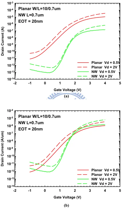
Compared with the planar device, NW device has better SS and negligible drain induce barrier lowering (DIBL) due to its ultra-thin channel body and superior gate controllability. Figure 3-1(b) shows the plot of drain current, normalized to the channel width, versus the gate voltage. Obviously, the NW device possesses larger drive current and lower off-current, hence its Ion/Ioff ratio is higher than that of the
planar one.
dimensions as a function of channel length. S1 to S4 devices are labeled in a dimensional order with S1 having the largest NW circumference and S4 the smallest. The TEM pictures of these devices are shown in Fig. 2-3. Even though the DIBL phenomenon is not as serious as the planar one, it still can be observed in the thicker NW devices. However, DIBL almost vanishes in the thinnest NW devices of S4. The DIBL effect is suppressed in S4 because of the better gate controllability and the fully depleted channel. In addition to DIBL, SS is also dependent on the dimension of channel. The impact of NW diameter on SS is illustrated in Fig. 3-3. Apparently, for a given channel length ( L = 0.4 µm ), SS becomes better when the diameter of channel becomes thinner. This result can be expected as the channel body gets narrower, the gate electrostatic control over the channel region gets stronger, so the SS is improved with decreasing NW’s cross-sectional feature size.
3.2 Program/Erase Characteristics
For the NW SONOS devices in this study, FN tunneling is employed for P/E operations as mentioned before. When the device is programmed, both source and drain are grounded and a positive voltage is applied to the gate and a large electric field will exist in the ONO region to induce FN tunneling. Before erasing, the device is programmed beforehand with 2.5 V shift of Vth relative to the fresh state.
Subsequently, a negative bias is applied to the gate and both source and drain are grounded. Figure 3-4 shows the ID-VG curve of a programmed NW device where the
SS is almost identical to the fresh state. Therefore, we can use the constant current method to extract the Vth. For simplicity, the Vth is defined as the gate voltage when
3.2.1 Program/Erase Characteristics of Planar and NW SONOS
In the previous section, we had observed that NW device owns better SS than the planar device, which can be attributed to its superior gate controllability. Accordingly, it is expected that the NW SONOS devices will have better P/E characteristics over the planar counterparts. Figure 3-5 illustrates the Vth shift versus programming and
erasing time of NW and planar SONOS with nominally identical ONO thickness. To compare the programming efficiency, we first consider the case when 13 V is applied as the stress bias for both planar and NW devices. When the operation time is merely 1 microsecond (µs), the Vth shift of NW and planar devices are about 2.4 V and 0 V,
respectively. Even when the programming time increases to 10 ms, Vth shift of planar
devices is still less than 0.3 V. Erase characteristics of NW and planar devices are shown in Fig. 3-5(b), which is very similar to the situation of program characteristics. When -11V is applied to the gate of the planar device for erasing, Vth shift is still
negligible after 1 s stress. On the contrary, the NW device biased with a gate voltage of -11 V can achieve about -2.5 V Vth shift after 1 ms.
From the aforementioned statements, NW SONOS devices indeed possess superior P/E speed to planar counterparts. Similar results of GAA NW SONOS devices had been discussed and reported in a recent publication [13]. The cross-sectional shape of the NW channel is nearly rectangular with rounded corner in this study. Here, to simplify the analysis, the shape of NW channel is considered to be cylindrical with the band diagrams shown in Fig. 3-6 to explain our findings. For a fair comparison, NW and planar SONOS devices have identical ONO thickness. The band diagrams of NW and planar SONOS devices, both of which are operating under program mode, with the same gate bias are shown in Fig. 3-6(a). The solid and dash lines represent the potential of planar and NW devices and the slope of the potential
line is proportional to the magnitude of electric field. Because of the cylindrical architecture of NW devices, the electric flux across the ONO layer is inversely proportional to the distance from the center of the NW. Consequently, the magnitude of electric field near the interface between tunneling oxide and channel is much higher than that in the planar one. In Chapter two, we had discussed the major factor that affects the FN tunneling current is the electric field. For that reason, the large electric field across the tunneling oxide enhances the electron tunneling probability and thus increases the program efficiency of NW SONOS devices when the applied gate bias is the same as the planar one. Similar to the programming case, the electric field as experienced by holes for tunneling from the channel to the oxide is increased due to the cylindrical geometry as shown in Fig. 3-6(b). Due to the higher electric field, the de-trapped rate of electrons in nitride also becomes faster in the NW devices. Therefore, GAA NW devices exhibit much larger P/E efficiency than planar devices.
3.2.2 Program Characteristics of NW SONOS
Figures 3-7(a) ~ (d) depict the Vth versus programming time for different splits of
GAA NW devices with gate biases of 8 V, 9 V, 10 V, 11 V, 12 V, 13 V, 14 V and 15 V, respectively. As shown in Fig. 3-7(a), the Vth shift increases when prolonging the
operation or increasing the gate bias due to the correspondingly higher electric field that will induce a larger FN tunneling current. During the programming process, the amount of electrons trapped in the nitride increases and the electric field across the tunneling oxide reduces. Therefore, the Vth becomes saturated and the programming
speed is retarded. This situation happens when the gate bias is 15 V and the stress time is longer than 10 ms for S1. For thinner devices, the programming saturation phenomenon occurs earlier for a specific programming voltage or at a lower
programming voltage for a specific programming time, as shown in Figs. 3-7 (b) ~ (d). This would limit the available window size for practical operation.
Figure 3-8 compares the program characteristics of NW SONOS devices of different dimensions with an identical programming voltage of 10 V. We separate this plot into two parts, Regions I and II, using the programming time of 10µs as demarcation. In Region I, where the programming time is shorter than 10 µs, we can easily observe that the thinner devices exhibit better programming efficiency. The potential profiles of NW SONOS devices with two different dimensions for the same gate bias are shown in Fig. 3-9(a). It can be seen that the voltage dropped across the tunneling oxide in thinner NW SONOS devices is higher than that in the thicker one due to its higher curvature which in turn induces a larger electric field. Hence the programming speed is faster than the thicker NW SONOS devices. In Region two, the net shift in Vth of S4 is smaller than 0.3 V and the other devices also become saturated
gradually. This can be explained by the band diagram which is shown in Fig. 3-9(b). During programming, the voltage drop across the blocking oxide gets larger as more electrons are trapped. Furthermore, the lower electric field across the tunneling oxide will decrease FN tunneling current from the channel. Therefore, when the rate of electron trapping is reduced and more electrons leak from nitride to the gate electrode, the Vth will become saturated. This situation is more obvious in thinner devices
because of their higher electric field across the blocking oxide. In this way, there are more electrons leaking to the gate and fewer electrons tunneling from the channel than the other devices with thicker NW. Thus, the magnitude of saturated Vth shift of
thinner devices is smaller than the thicker ones. The program speed characteristics for NW SONOS devices of different dimensions with an identical gate bias of 14 V are shown in Fig. 3-10. Owing to the high gate voltage applied and the limitation in time
resolution of the measurements (10-7 sec), the initially fast rise in Vth cannot be
resolved and only Region II is seen.
3.2.3 Erase Characteristics of NW SONOS
Figures 3-11(a) ~ (d) show erase speed characteristics for NW SONOS devices of different dimensions with gate bias of -8 V, -9 V, -10 V, -11 V, -12 V and -13 V, respectively. The increase magnitude in gate bias (absolute value) does apparently accelerate the erase speed. The value of Vth shift also increases with the operation
time. In Fig. 3-11(a), the rate of Vth shift slows down when erasing time is longer than
10 ms with gate bias of -11 V due to the fact that the amount of the trapped electrons in the nitride does not decrease proportionally with erasing time. Erase saturation happens when the gate bias is larger than 13 V because some electrons inject from the gate electrode. Figure 3-12 compares the erase speeds for NW SONOS devices of different dimensions with an identical gate bias of -9 V. We can clearly observe that the thinner devices possess faster erase speed. Figure 3-13 illustrates the band diagrams during erasing. Thinner device has higher electric field across the tunneling oxide which can induce larger tunneling current of holes. Furthermore, higher electric field also prompts more electrons to be de-trapped from nitride into the channel.
3.3 Reliability Characteristics of Planar and NW SONOS
3.3.1 Endurance
For the endurance tests, different P/E conditions were applied to different devices to obtain a comparable initial memory window (~2 V). Figure 3-14 indicates that the memory window is still acceptable after 104 stressing cycles. As the cycle
number increases, the Vths are almost unchanged in the programmed state and move
upwards gradually in the erased state for these four devices, which implies that a few electrons still remain in the trapping layer when erasing. Consequently, residual electrons lead to an increasing Vth. Figure 3-15 shows the ID-VG curves of the S1
device before and after 104 P/E cycles with P/E conditions of 11V 100 µs/-10 V 1 ms. It is clear that the SS is nearly identical to the fresh state after 104 P/E cycles. This indicates the tunneling oxide is not seriously degraded during the P/E cycles.
3.3.2 Retention
To measure the retention characteristics, we chose appropriate P/E conditions for each device to achieve a comparable initial memory window. Figure 3-16 shows the retention of NW SONOS devices with an initial window of about 2 V. The memory windows of S1, S2, S3 and S4 after 10 years are about 1.8, 0.8, 0.5 and 0.2 V, respectively. It demonstrates that the thinner devices exhibit worse data retention. In previous chapter, we had discussed the relation between the leakage current and electric field. When electrons are trapped in the nitride layer, these electrons will induce electric field in the ONO layers. In thinner devices, higher electric field induces a larger leakage rate. Furthermore, thinner devices need fewer electrons to reach the same memory window. The same amount of leaked electrons may cause a greater impact for the thinner devices. Consequently, the thicker devices have better data retention characteristics than thinner ones
Chapter 4
Characteristics of SONOS Devices with
In-Situ Embedded Silicon Nanocrystals
In this chapter, basic transfer characteristics of standard (STD) and Si NCs NW SONOS devices will be compared in the first section. Next, the P/E characteristics and reliability issues of Si NCs NW SONOS devices will be examined and compared with the STD NW SONOS devices.
4.1 Basic Transfer Characteristics
The ID-VG curves of STD and Si NCs NW SONOS devices are shown in Fig. 4-1.
All measured devices in this figure have channel length of 0.4 µm and the wire diameter of 30nm as shown in Fig. 2-13. Thickness of the ONO of the STD NW SONOS is 3.5/8/12 nm. For the Si NCs devices, we keep the thickness of tunneling oxide, nitride and blocking oxide as the same as the STD NW SONOS. The Si NCs are placed at different positions as mentioned before in Section 2.3. We call these devices as the bottom, mid or top Si NCs NW SONOS for the Si NCs located at the interface of tunneling oxide and nitride layer, in the nitride layer or between the nitride and blocking oxide, respectively. The SONOS device without Si NCs is relatively superior in terms of SS behavior which can be seen in Fig. 4-1. The discrepancy of SS between STD and Si NCs SONOS devices can be explained by the following two reasons. First, after depositing the Si NCs, the surface is unsmooth as
indicated by the AFM image shown in Fig. 2-9. Consequently, the effective oxide thickness of the Si NCs NW SONOS is not uniform across all gated area, which may lead to the worse SS. Second, embedded Si NCs will increase the effective oxide thickness because we didn’t change the thickness of TEOS oxide and nitride layers. Therefore, the SS of STD NW SONOS device is better than that of the Si NCs NW SONOS devices.
4.2 Program/Erase Characteristics
The manners we used here to program and erase the STD and Si NCs devices were the same as we had described in Section 3.1. Before erasing, these devices were all programmed beforehand with 2.5 V shift of Vth relative to the fresh state.
4.2.1 Program Characteristics of STD and Si NCs NW SONOS
Figures 4-2 (a) ~(d) depict the Vth shift versus programming time for STD and Si
NCs NW SONOS devices with gate biases of 9 V, 10 V, 11 V, 12 V, 13 V, 14 V and 15 V, respectively. The Vth shift increases when prolonging the operation time or
increasing the gate bias for either STD or Si NCs device. Programming saturation, which has been explained in Section 3.2.2, also occurs in these devices. However, the Vth shift behaviors of Si NCs device are very dissimilar to the STD counterparts.
Figure 4-3 compares the program characteristics of STD and bottom Si NCs NW SONOS devices with the program voltages of 9 V, 11 V and 13 V. Compared with the STD device at gate bias of 9 V, the Vth shift of the bottom Si NCs device is smaller
before the programming time reaches 100 µs. However, because of the larger increasing rate of the bottom Si NCs device during the whole programming process, the bottom Si NCs device shows larger Vth shift and increasing rate of Vth when 13 V
is applied to the gate, Obviously, the intersection of the Vth shift lines between STD
and Si NC devices happens earlier when the gate bias is increased. The potential profiles of STD and bottom Si NCs NW SONOS devices, biased at the same gate voltage, are shown in Fig. 4-4. The dash and solid lines represent the potential of STD and Si NCs devices, respectively. Owing to the fact that EOT of the bottom Si NCs device is larger than the STD device, at the beginning of the programming process, the electric field across the tunneling oxide in STD NW SONOS is higher than that in the bottom Si NCs NW SONOS and will raise the tunneling probability of electrons. However, the faster increasing rate of Vth shift for the bottom Si NC devices is due to
the influence of Si NCs. According to the gate-sensing and channel-sensing method proposed by H. T. Lue et al. [45], the mean location of the trapped electrons migrates from the interface of the tunneling oxide and nitride toward the center of nitride layer in STD devices. Furthermore, the mean location shift to the center of nitride becomes faster when the program bias gets larger as shown in Fig. 4-5. Such situation can be changed with Si NCs embedded between the tunneling oxide and nitride layer which can be considered as additional quantum wells formed at the tunneling oxide/nitride interface that improve the trapping efficiency and make the mean location of the trapped electrons closer to the channel. Therefore, equal amount of trapped electrons will induce higher Vth shift in the bottom Si NCs device. Furthermore, the available
trapping sites also increase due to the incorporation of the Si NCs as evidenced by the larger Vth shift in Fig.4-3.
In Fig. 4-6, we illustrate and compare the program characteristics of STD and mid Si NCs NW SONOS devices with the gate voltages of 9 V, 11 V and 13 V. Due to a larger EOT and thus a weaker electric field, the shift in Vth for the Si NCs samples is