國
立
交
通
大
學
電機學院微電子奈米科技產業研發碩士班
碩
士
論
文
可寫入抹除高介電常數氮氧化鉿
金屬-絕緣層-矽 電容
A Program-Erasable High-κ Hf
3
N
2
O
5
Metal-Insulator-Silicon Capacitor
研 究 生:林俊賢
指導教授:荊鳳德 教授
中 華 民 國 九 十 七 年 一 月
可寫入抹除高介電常數氮氧化鉿
金屬-絕緣層-矽 電容
A Program-Erasable High-κ Hf
3N
2O
5Metal-Insulator-Silicon Capacitor
研 究 生:林俊賢 Student:Chun-Hsien Lin
指導教授:荊鳳德 Advisor:Albert Chin
國 立 交 通 大 學
電機學院微電子奈米科技產業研發碩士班
碩 士 論 文
A ThesisSubmitted to College of Electrical and Computer Engineering National Chiao Tung University
in partial Fulfillment of the Requirements for the Degree of
Master in
Industrial Technology R & D Master Program on Microelectronics and Nano Sciences
January 2008
Hsinchu, Taiwan, Republic of China
可寫入抹除高介電常數氮氧化鉿 金屬-絕緣層-矽 電容
學生:林俊賢
指導教授:荊鳳德
國立交通大學電機學院產業研發碩士班
摘
要
記憶體電容是決定檢測訊號電壓、速度、資料保存時間、耐久性以及防止軟性誤差 的重要參數。然而隨著超大型積體電路技術不斷的微縮,電容面積勢必隨之遞減,以期 達到減少元件尺寸及降低成本的需求,但此舉將減低電容厚度造成不必要的漏電流,為 了解決此問題,傳統的二氧化矽將被高介電常數材料所取代,以達高電容密度及降低漏 電流,此外記憶體電容也渴望具有可寫入抹除和良好資料保存等特性。 本文將探討使用高介電常數氮氧化鉿為介電層的 可寫入抹除 金屬-絕緣層-矽 結 構電容,其可應用在記憶體上例如:動態隨取記憶體(DRAM)與快閃記憶體(Flash)。此元 件具有高電容密度約 6.5 fF/μm2 、低寫入-抹除電壓 ±5V、大記憶體視窗 1.5V 以及優異 資料保存特性。此外經由漏電流特性分析計算出其蕭基能障與電子捕捉能階,發現氮氧 化鉿蕭基能障為 0.69~0.7 eV 且具有較深的電子捕捉能階約 1.01~1.05 eV。
ii
A Program-Erasable High-
κ Hf
3N
2O
5Metal-Insulator-Silicon Capacitor
student:Chun-Hsien Lin Advisor:Dr. Albert Chin
Industrial Technology R & D Master Program of
Electrical and Computer Engineering College
National Chiao Tung University
ABSTRACT
Memory cell capacitance is the crucial parameter which determines the sensing signal voltage, speed, data retention times, endurance and against the soft error event. However, the very large scale integration (VLSI) technology is continues down-scaling of the size of capacitors to reduce chip size and the cost. It will decrease dielectric thickness and result in the undesired leakage current. To solve this problem, the conventional silicon dioxide will be replaced with high dielectric constant (high-κ) materials to increase the capacitance density and degrade the leakage current. Besides, capacitors also desire both good data retention and program-erasable capability for memory applications.
In this study, we demonstrate a programmable-erasable MIS capacitor with a single high-κ Hf3N2O5 dielectric layer for many applications such as volatile DRAM and non-volatile MONOS type memories. This device showed a capacitance density of ~ 6.5 fF/μm2, low program and erase voltages of +5 and -5 V, and a large ΔVth memory window of 1.5V. In
addition the 25oC data retention was good, as in program and erase decay rates of only 2 and 6.2 mV/dec. In addition, we found a deep trapping level of 1.01~1.05 eV from measured J-V characteristics. The electrodes displayed a Schottky barrier height of 0.69~0.7 eV.
致謝
首先我要感謝指導教授 荊鳳德博士,兩年來不辭辛苦的指導與教誨,以致在研究技 巧與知識上能不斷的充實精進,此外更要感謝您時常的鼓勵與督促,使研究進度能順利的 進行與完成,在此由衷的獻上感謝與祝福。 在研究室的生活中,我要特別感謝楊學人學長,謝謝你亦師亦友的訓練與幫助,讓我 得以順利的完成碩士論文。再來,我要感謝淳護學長、存甫學長、建宏學長以及實驗室的 學長姐們,謝謝你們不分晝夜的實驗儀器訓練與提供見解。再者同學中謝謝冠麟、偉倫、 建弦、群懿及佩諭,有你們無私的幫忙與熱切的討論,無論在修課、研究以及生活上都 充滿了歡樂與鼓舞。也謝謝實驗室成員們有你們才使 ED 633 室能充滿溫馨與色彩。 最後,我要對我的父親 英輝先生、母親 秀珠女士以及家人們獻上最真摯的祝福與 感恩,有你們的栽培、支持與鼓勵才有今日的表現。僅將此論文獻給你們,與你們分享 這喜悅,再一次感謝一路上所有幫助我的人。iv
Contents
Abstract (in Chinese)
……….……….……….………....iAbstract (in English)
………...iiAcknowledgement (in Chinese)
……….………iiiContents
……….……….………….…………...ivFigure Captions
……….……….……….……...vChapter 1 Introduction
1.1
Motivation to study high-κ dielectrics……….11.2
Overview of high-κ dielectrics………...31.3
Hafnium-based dielectrics………....51.4
Schottky Emission and Pool-Frenkel Emission……….…………...8Chapter 2 The Experimental Steps and Measurement
2.1
Fabrication of MIS capacitors……….……….……….………252.2
The measurement of MIS capacitors ………..……….….26Chapter 3 Result and Discussion
3.1
Memory characteristics of Hafnium oxynitride capacitors………333.2
Energy barrier and trap energy level………..363.3
The applications of MIS capacitors…...38Chapter 4 Conclusion
………...……52References
………...54Figure Captions
Chapter 1 Introduction
Fig. 1-1
The International Technology Roadmap for semiconductor 2006………...15Fig. 1-2
The values of work function for different metal materials………...16Fig. 1-3
Comparison of relevant properties for high-κ candidates……….17Fig. 1-4
The leakage current of Hafnium oxynitride with different N2 flow rate conditions as depositing……….18Fig. 1-5
Thin film XRD spectra with a glancing angle of 30 as a function of PDA temperature for HfO2 and Hf1-x-yNxOy films on Si substrates………..19Fig. 1-6
A Schottky barrier formed by contacting an n-type semiconductor with a metal having a larger work function: (a) band diagrams for the metal and the semiconductor before joining; (b) equilibrium band diagram for the junction……20Fig. 1-7
Schottky barrier between a p-type semiconductor and a metal having a smaller work function: (a) band diagram before joining; (b) band diagram for the junction at equilibrium………21Fig. 1-8
Image charge and electric field lines at a metal-dielectric interface………22Fig. 1-9
(a) Distortion of the potential barrier due to image forces with zero electric field; (b) with a constant electric field……….23Fig. 1-10
Pool-Frenkel emission from trapped electrons……….24Chapter 2 The Experimental Steps and Measurement
Fig. 2-1
The RCA clean steps……….27Fig. 2-2
Silicon substrate………28Fig. 2-3
RCA Clean………28Fig. 2-4
Deposited Hf1-x-yNxOy dielectric………...…29vi
Fig. 2-6
Photoresist and Lithography……….30Fig. 2-7
Lithography Patterned………...30Fig. 2-8
Deposited TaN by PVD………....31Fig. 2-9
Fabricated MIS capacitors………31Fig. 2-10
IV and CV measurement………...32Chapter 3 Result and discussion
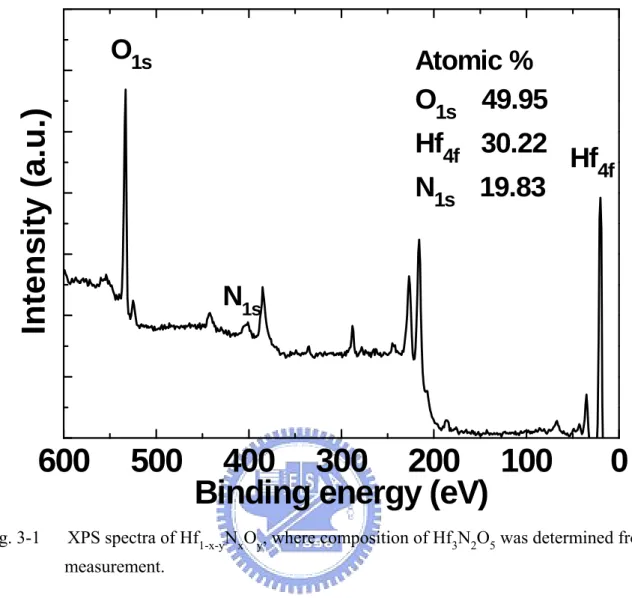
Fig. 3-1
XPS spectra of Hf1-x-yNxOy, where composition of Hf3N2O5 was determined from measurement……….40Fig. 3-2
The C-V characteristics of a TaN/Hf3N2O5/Si MIS device which shows large hysteresis………..41Fig. 3-3
The C-V characteristics of an Hf3N2O5 MIS capacitor after applying a ± 5 V program/erase (P/E) voltage for various periods from 0.1 to 100 ms………..42Fig. 3-4
The threshold (Vth ) voltage for various P/E voltages from ± 3 to ± 5 V, as a function of the P/E time………43Fig. 3-5
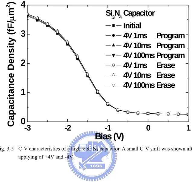
C-V characteristics of a high-κ Si3N4 capacitor. A small C-V shift was shown after applying of +4V and -4V………..44Fig. 3-6
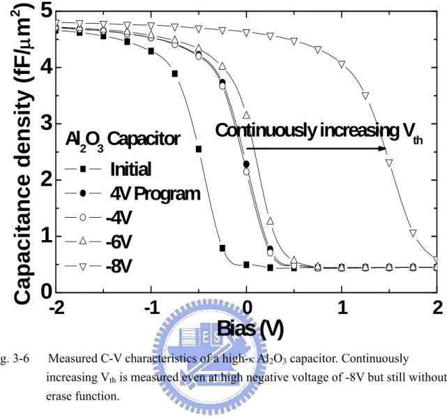
Measured C-V characteristics of a high-κ Al2O3 capacitor. Continuously increasing Vth is measured even at high negative voltage of -8V but still without erase function……….45Fig. 3-7
Retention characteristics at 25 and 100oC of an Hf 3N2O5 MIS capacitor, measured to 10000 s, after the 1 ms, ± 5 V P/E writing pulse. The data for an AlN MIS capacitor are shown for comparison……….46Fig. 3-8
The J-V characteristics of a TaN/Hf3N2O5/Si MIS device. The lines are fits to SE or FP models using eq. (3.1)……….47Fig. 3-9
A ln(J/T2)-E1/2 plot and SE calculations for TaN/Hfelectric field with electron injection from either lower Si or upper TaN
electrodes………..48
Fig. 3-10
The ln(J/E)-1/kT plots and FP calculations of bottom injection for TaN/Hf3N2O5/Sidevice data at high field………49
Fig. 3-11
The ln(J/E)-1/kT plots and FP calculations of top injection for TaN/Hf3N2O5/Sidevice data at high field………50
Fig. 3-12
Band diagram of Hf3N2O5 MIS devices. The barrier height and trap energy wereobtained from SE and FP model calculations to the measured ln(J/T2)-E1/2 and
1
Chapter 1
Introduction
1.1 Motivation to study high-
κ dielectrics
The industry’s demand for greater integrated circuit functionality and performance at lower cost requires an increased circuit density, which has translated into a higher density of transistors on a wafer. This rapid shrinking of the transistor feature size has forced the channel length and gate dielectric thickness to also decrease rapidly. However, the scaling trend of MOSFETs devices will produce the large leakage current due to thinner gate oxide [1.1]. To reduce the leakage current related higher power consumption in highly integrated circuit and overcome the physical thickness limitation of silicon dioxide, the conventional SiO2 will be replace with high dielectric constant (high-κ) materials as the gate dielectrics beyond the 65nm technology mode [1.2]-[1.7]. Therefore, the engineering of high-κ gate dielectrics have attracted great attention and played an important role in technology pull for VLSI. Although high-κ materials often exhibit smaller band gap and higher defect density than conventional silicon dioxide, using the high-κ gate dielectric can increase efficiently the physical thickness in the same effective oxide thickness (EOT) that shows lower leakage characteristics than silicon dioxide by several orders without the reduction of capacitance density [1.3]-[1.6].
According to the ITRS (International Technology Roadmap for Semiconductor) [1.8], the thickness of gate oxide has to be below 10Å after 2008. Besides, the suitable gate dielectrics must have κ value more than 8 for 50-70 nm technology nodes and that must be more than 15 when the technology dimensions less than 50 nm. Fig. 1-1 shows the evolution of MOSFET technology requirement.
As an alternative to oxide/nitride systems, much work has been done on high-κ metal oxides as a means to provide a substantially thicker (physical thickness) dielectric for reduced leakage and improved gate capacitance. In the search of finding suitable high-κ gate dielectrics for use beyond oxynitride systems, several approaches have been used in fabricating potential materials candidates. To find out the suitable high-κ dielectrics are significant task to the next VLSI generation.
3
1.2 Overview of high-
κ dielectrics
Many of the materials initially chosen as potential alternative gate dielectric candidates were inspired by memory capacitor applications and the resultant semiconductor manufacturing tool development infrastructure. The most commonly studied high-κ gate dielectric candidates such as Ta2O5, SrTiO3, and Al2O3 which have dielectric constants ranging from 10 to 80, and have been employed mainly due to their maturity in memory capacitor applications. With the exception of Al2O3, however, these materials are not thermodynamically stable in direct contact with Si [1.1]. Moreover, the oxides should preferably be amorphous and able to withstand processing at high temperatures of up to 1000 °C. The leading contenders are the Hf, Zr, and La oxides. However, these oxides are not good glass formers like SiO2 and they tend to crystallize well below 800 °C. Silicates or aluminates can be used instead of oxides as they crystallize much less easily, but at the expense of a lower κ [1.9].
The gate electrode in CMOS devices is traditional made of polysilicon. However, as the technology down-scaling, device performance and reliability can be seriously degraded by the intolerably high direct-tunneling leakage current, increased gate resistance, worsened polysilicon gate depletion, and boron penetration [1.12]-[1.13]. To alleviate these problems, a high dielectric constant (high-κ) gate insulator and metal gate have been proposed to meet the stringent performance requirement. For the high-κ dielectrics, replacing the conventional
polysilicon gate electrode with metal gate has been proposed because of the interface instability between the high-κ dielectrics and polysilicon gate [1.10]. The work function (Φm)
of metal (in Fig. 1-2) play an important role for metal-gate/high-κ MOSFET. The preferred work function of the metals are ~5.1 eV for p-MOSFETs and ~4.2 eV for n-MOSFETs. Refractory metal nitrides such as tantalum nitride (TaN) and titanium nitride (TiN) have been extensively investigated as the potential solutions to replace poly-Si [1.11].Tantalum (Ta) has a work-function close to n+ poly-Si. Tantalum nitride (TaN) is quite stable (to maintain thermal stability up to a 1000oC RTA) because the activation energy of metal and nitrogen is relatively low. Tantalum is bonded tightly within nitride and no diffuse was observed in fabricated devices.
In conclusion, a systematic consideration of the required properties of gate dielectrics indicates that the key guidelines for selecting an alternative gate dielectric are (a) permittivity, band gap, and band alignment to silicon, (b) thermodynamic stability, (c) film morphology, (c) interface quality, (e) compatibility with the current or expected materials to be used in processing for CMOS devices, (f) process compatibility, and (g) reliability. Many dielectrics appear favorable in some of these areas, but very few materials are promising with respect to all of these guidelines. Fig. 1-3 summarizes the properties for high-κ candidates.
5
1.3 Hafnium-based dielectrics
Hafnium-based dielectrics, including HfO2 [1.14]-[1.15], HfON [1.16]-[1.17], HfSiO [1.18], HfSiON [1.19], HfAlO, and HfAlON [1.20]-[1.22] have gained significant attention in recent years as a replacement for SiO2 in complementary-metal-oxide semiconductor (CMOS) devices. Among them, HfO2 is very promising for the next-generation gate dielectric of MOSFETs, because of its high dielectric constant, excellent thermal stability, wide band gap, and large band offsets. However, the high oxygen and impurities penetration and boron diffusion into the gate dielectric should be suppressed to maintain low equivalent oxide thickness (EOT), reduce flatband voltage fluctuation; and further it demonstrated a well crystallized structure after annealing at low temperature around 500℃ [1.23].
Several studies have focused on the improvement of the thermal stability of high-κ gate dielectric to overcome the insufficient immunity to oxygen or impurity diffusion during the subsequent thermal process. Those studies incorporated Al, Si, and N into Hafnium oxide to form HfON, HfSiO, HfSiON, HfAlO, and HfAlON respectively. Among them, HfSiON, hafnium silicon oxynitride which was found to improve thermal stability further compared to HfON. However, dielectric constants are reduced in HfSiON due to the presence of silicon oxide bonds with much lower dielectric constant than HfO2. HfSiON with optimized composition remained amorphous state up to 1100 0C whereas dielectric constant decreased down to ~10. In terms of application, the HfSiON appears to be very promising materials for
the low power devices rather than high speed device requiring further scaling-down of EOTs <10Å in the near future. In conclusion, the addition of Al and Si has been known to retard crystallization of HfO2, but the dielectric constant is degraded as the Al or Si content increases [1.23]-[1.31].
Hf1-x-yNxOy appears to be promising for further scaling-down of EOT since incorporated nitrogen does not degrade dielectric constant of the film. Hf1-x-yNxOy showed a lower leakage current than HfO2. Fig. 1-4 shows the leakage current of Hafnium oxynitride with different N2 flow rate conditions as depositing. It shows Hf1-x-yNxOy for N2 flow rate at 50% almost 2 order lower leakage current than HfO2 at -2V. The lower leakage current of Hf1-x-yNxOy can be attributed to its thicker physical thickness to achieve a given EOT due to the higher dielectric constants of bulk and interface layer compared to HfO2. (Dielectric constant of bulk for HfO2 and Hf1-x-yNxOy are 19 and 22, and the dielectric constant of interfacial layer in Hf1-x-yNxOy ~14 is larger than that of HfO2 ~7.8) [1.23]-[1.31].
Nitrided films show improved thermal stability, inhibited crystallization, improved electrical and dielectric properties, and decreased dopant, oxygen, and silicon interlayer diffusion when compared to hafnium silicates. It was due to the atomic [N] could passivate [O] vacancies in the gate dielectrics during nitridation process and remove electron leakage path mediated by [O] vacancies. Thin film XRD with a glancing angle of 30 was used to investigate crystalline of HfO2 and Hf1-x-yNxOy on Si substrates. Fig.1-5 depicts XRD spectra
7
of HfO2 and Hf1-x-yNxOy films which were annealed under N for 1 min at various temperatures ranging from500℃ to 950℃. Hf1-x-yNxOy showed an increase of 300℃ in crystallization temperature compared to HfO2. It was due to Hf-N bond has higher thermal stability than Hf-O bond. Although, recent reports have indicated that the nitrogen introduces energy levels in the band gap of HfO2, thereby reducing the valence-band offset of the dielectric on silicon. It concludes that both band gap and band offset of hafnium oxynitrides are reduced by a fixed amount regardless of nitrogen concentration. However, these offsets result in barrier heights that are still sufficient to make Hf1-x-yNxOy a viable high-κ for gate dielectric applications while taking advantage of the improved physical and electrical properties [1.23]-[1.31].
Although Hf1-x-yNxOy crystallizes around ~800oC not high enough to remain amorphous phase in the conventional self-aligned source/drain process, and reduce the band offset ,but it provide higher scalability than HfSiON due to its higher dielectric constant ~22.Therefore, it is worth further studying on the electrical and material characterization of Hf1-x-yNxOy film [1.23]-[1.31].
1.4 Scotty Emission and Pool-Frenkel Emission
Schottky Barrier:
The ideal energy band diagram for a particular metal and n-type semiconductor before making contact is shown in Fig.1-6. The vacuum level is used as a reference level. The parameter
m
φ is the metal work function (measured in volts), φ is the semiconductor work s function, and χ is known as the electron affinity. Now, we have assumed thatφm >φs. The
ideal thermal-equilibrium metal-semiconductor energy-band diagram can be observed, for this situation. Before contact, the Fermi level to become a constant through the system in thermal equilibrium, electrons from the semiconductor flow into the lower energy states in the metal. Positively charged donor atoms remain in the semiconductor, creating a space charge region. The parameter φ is the ideal barrier height of the semiconductor contact, the potential B0 barrier seen by electrons in the metal trying to move into the semiconductor. This barrier is known as the Schottky barrier and is given, ideally by
φB0 =(φm −χ) (1.1)
On the semiconductor side, Vbi is the built-in potential barrier, similar to the case of the pn junction, is the barrier seen by electrons in the conduction band trying to move into the metal. The built-in potential barrier is given by
Vbi =φB0 −φn (1.2)
which makes Vbi a slight function of the semiconductor doping, as was the case in a pn junction. Fig. 1-6 shows Schottky barrier formed by contacting an n-type semiconductor with a metal having a larger work function and Fig. 1-7 shows Schottky barrier between a p-type semiconductor and a metal having a smaller work function [1.36].
9
If we apply a positive voltage to the semiconductor with respect to the metal, the semiconductor-to-barrier height increases, while φ remains constant in this idealized case. B0 This bias condition is the reverse bias. If a positive voltage is applied to the metal with respect to the semiconductor, the semiconductor-to-metal barrier Vbi is reduced while φ again B0 remains essentially constant. In this situation, electrons can more easily flow from the semiconductor into the metal since the barrier has been reduced. This bias condition is the forward bias. We expect the current-voltage characteristics of the Schottky barrier junction to be similar to the exponential behavior of the pn junction diode. The current mechanism here, however, is due to the flow of majority carrier electrons. In forward bias, the barrier seen by the electrons in the semiconductor is reduced, so majority carrier electrons flow more easily from the semiconductor into the metal. The forward-bias current is in the direction from metal to semiconductor; it is an exponential function of the forward-bias voltage [1.32].
Schottky Effect:
The Schottky effect or image force induced barrier lowering effect is due to an electron in a dielectric at a distance x from the metal will create an electric field. The field lines must be perpendicular to the metal surface and will be the same as if an image charge+e is located at the same distance from the metal surface, but inside the metal. This image effects is shown in Fig. 1-8. The force on the electron due to the coulomb attraction with the image charge is
( )
eE x e F s − = − = 2 2 2 4πε (1.3)The potential can then be found as
( )
( )
∫
∫
∞ ∞ − = ⋅ + = + = − x x s xx e dx x a e Edx x πε πε φ 16 ' ' 4 ' 2 (1.4)Where x is the integration variable and where we have assumed that the potential is zero at'
∞ =
x .
The potential energy of the electron is −eφ
( )
x ; Fig.1-9 (a) is a plot of the potential energy assuming that no other electric fields exist. With an electric field present in the dielectric, the potential is modified and can be written as
( )
x s E x e x = − − − πε φ 16 (1.5)The potential energy of the electron, including the effect of a constant electric field, is plotted in Fig. 1-9(b). The peak potential barrier is now lowered. This lowering of the potential barrier is the Schottky effect, or image-force-induced lowering.
We can find the Schottky barrier lowering,Δ , and the position of the maximum barrier, φ
m
x , from the condition that
( )
(
)
=0 dx x e d φ (1.6) We find that E e x s m = 16πε (1.7) And s e πε φ 4 = Δ (1.8)11 energy barrier to emission is φox−Δφ [1.32].
Schottky Emission:
The current transport in a metal-semiconductor junction is due to mainly to majority carries as opposed to minority carriers in a pn junction. The basic process in the rectifying contact with an n-type semiconductor is by transport of electrons over the potential barrier, which can be described by the thermionic emission theory [1.32].
The thermionic emission characteristics are derived by using the assumptions that the barrier height is much larger than Tκ , so that the Maxwell-Boltzmann approximation applies and that thermal equilibrium is not affected by this process. The current Js→m is the electron
current density due to the flow of electrons from semiconductor into the metal, and the current
s m
J → is the electron current density due to the flow of electrons from the metal into the semiconductor. The subscripts of the currents indicate the direction of electron flow. The conventional current direction is opposite to electron flow.
The current density Js→m is a function of the concentration of electrons which have
x-directed velocities sufficient to overcome the barrier. We may write
∫
∞→s
=
E' xm
e
v
dn
J
(1.9) Where 'E is minimum energy required for thermionic emission into the metal, υ is the x carrier velocity in the direction of transport, and e is the magnitude of the electronic charge.
The incremental electron concentration is given by
dn= gc
( ) ( )
Ef
F E dE (1.10)Where gc(E) is the density of states in the conduction band and fF(E) is the Fermi-Dirac
probability function. Assuming that the Maxwell-Boltzmann approximation applies, we may write
(
)
dE T E E E E h n dn F Cm
⎥⎦ ⎤ ⎢⎣ ⎡− − − ⎟ ⎠ ⎞ ⎜ ⎝ ⎛ ∗ = κ π exp 2 4 3 2 3 (1.11) If all of the electron energy above Ec is assumed to be kinetic energy, then we havemnv = E−Ec ∗ 2
2 1
(1.12) The net current density in the metal-to-semiconductor junction can be written as J = Js→m −Jm→s (1.13)
which is defined to be positive in the direction from the metal to the semiconductor. We find that ⎥⎦ ⎤ ⎢ ⎣ ⎡ − ⎟ ⎠ ⎞ ⎜ ⎝ ⎛ ⎥ ⎦ ⎤ ⎢ ⎣ ⎡ ⎟ ⎠ ⎞ ⎜ ⎝ ⎛ − = ∗ 2exp 0 exp 1 T eV T e T A J B a κ κ φ (1.14) where 3 2 4 h k em A∗≡ π n∗ (1.15) ⎟⎟⎠ ⎞ ⎜⎜ ⎝ ⎛ = 0 * 120 m mox (1.16)
13
emission. We can although change the expression in another form
⎥ ⎥ ⎥ ⎥ ⎥ ⎦ ⎤ ⎢ ⎢ ⎢ ⎢ ⎢ ⎣ ⎡ ⎟⎟ ⎠ ⎞ ⎜⎜ ⎝ ⎛ − − = ∗ T qE q T A J r B SE κ ε πε φ 0 0 2exp 4 (1.17) Pool-Frenkel Emission:
Pool-Frenkel effect is also possible conduction mechanism and in fact it is observed very often in all high-κ materials. This mechanism is appearing with field enhanced electron emission from Columbic centers, i.e. it is bulk-limited [1.33].
The Pool-Frenkel emission is due to field-enhanced thermal excitation of trapped electrons into the conduction band. For trap states with coulomb potentials, ignoring the effect of finite temperature and image-force-induced barrier lowering [1.34], the expression is virtually identical to that of the Schottky emission. The barrier height, however, is the depth of the trap
potential well, and the quantity
i q
πε is larger than in the case of Schottky emission by a
factor of 2, since the barrier lowering is twice as large due to the immobility of the positive charge. Fig.1-10 illustrates the Pool-Frenkel emission.
⎥ ⎥ ⎥ ⎥ ⎥ ⎦ ⎤ ⎢ ⎢ ⎢ ⎢ ⎢ ⎣ ⎡ ⎟ ⎟ ⎠ ⎞ ⎜ ⎜ ⎝ ⎛ − − = ∗ kT qE q E B J r t PF 0 exp πε ε φ (1.18) where
B =qNCu
∗
(1.19)
t
φ is the energy level of trapping center.
Pool-Frenkel emission occurs more often than not while depositing oxide by PVD or CVD methods because of the more defects in the insulator [1.35].
15
Fig.11-3 Comparison of reelevant prop
17
Fig.1-4 The leakage current of Hafnium oxynitride with different N2 flow rate conditions as depositing.
Fig.1-5 tem HfO Thin film X mperature f O2 2θ XRD spectr for HfO2 an 19 ra with a gla nd Hf1-x-yNxO H ancing angl Oy films on Hf1-x-yNxOy le of 30 as a Si substrate 2θ function of es[1.23]. f PDA
(a)
(b)
Fig.1-6 A Schottky barrier formed by contacting an n-type semiconductor with a metal having a larger work function: (a) band diagrams for the metal and the
semiconductor before joining; (b) equilibrium band diagram for the junction.
Metal Silicon qψm qψs qχ ψm>ψs n-type Ec Ev EFs EFm Ec EFs Ev EFm W qψB=q(ψm-χ) qV0=q(ψm-ψs) ++ + -- - n Metal Silicon
21
(a)
(b)
Fig.1-7 Schottky barrier between a p-type semiconductor and a metal having a smaller work function: (a) band diagram before joining; (b) band diagram for the junction at equilibrium. Ec Ev EFs EFm Metal Silicon qψm qψs qχ ψm<ψs p-type ++ + -- - p Metal Silicon qV0=q(ψs-ψm) Ec EFs Ev W
Fig.1-8 Image charge and electric field lines at a metal-dielectric interface
x
+
-
Metal
Dielectric
23
(a)
(b)
Fig.1-9 (a) Distortion of the potential barrier due to image forces with zero electric field;
(b) with a constant electric field.
EF x E(x) EF x E(x) eψB0 Δψ eψBn eE xm x=0
Fig.1-10 Pool -Frenkel emission from trapped electrons.
Metal
Insulator
Silicon
25
Chapter 2
The Experimental Steps and Measurement
2.1 Fabrication of MIS capacitors
The MIS capacitor used a standard 4-in P-type silicon wafer (100) as the substrate, and following RCA clean processes. Fig. 2-1 shows the steps of RCA clean in detail. After standard pre-gate clean, an 30nm Hf1-x-yNxOy dielectric was deposited with high N2 flows by DC sputtering of Hf target in Ar + N2 +O2 mixed gas ambient at a sputtering power of 150W. The total gas pressure was kept as 7.6 mTorr during the sputtering process. The dielectric was then Post Deposition Anneal (PDA) at 650℃ for 30s under N2 ambient to reduce defects. A TaN layer was deposited by PVD and then gate patterned by photo lithography to form top electrode with capacitor area of 100μm × 100 μm. Finally, TaN/ Hf1-x-yNxOy/silicon stacked metal-insulator-silicon (MIS) capacitors were fabricated. The processes of MIS capacitors is shown in Fig. 2-2 ~ Fig. 2-10. For comparison, we also fabricated Al2O3 and Si3N4 capacitors.
2.2 The measurement of MIS capacitors
To investigate the electrical characteristics of devices, we measured the Ig-Vg curves for gate leakage current by using HP 4156C semiconductor parameter analyzer. Besides, HP4284A precision LCR meter was used to evaluate the gate capacitance and the conductance ranging from 100 kHz to 1 MHz. For memory measurement, the fabricated MIS devices were characterized by program and erase measurements, as well as retention tests at 25℃ and 100℃ using an HP4156C Semiconductor Parameter Analyzer and HP8110A 150 MHz Pulse Pattern Generator.
27
A. DI water rinse, 5 min.
B.
H
2SO
4: H
2O
2= 3:1, (10 min, 75~85℃)
C. DI water rinse, 5 min.
D. HF : H
2O = 1:100
E. DI water rinse, 5 min.
F. NH
4OH : H
2O
2: H
2O = 1:4:20 (SC1), (10 min,75~85℃)
G. DI water rinse, 5 min.
H. HCl : H
2O
2: H
2O = 1:1:6 (SC2), (10min, 75~85℃)
I. DI water rinse, 5 min.
J. HF : H
2O = 1:100
K. DI water rinse.
L. Spinner
P-type
P-type
RCA Clean
Fig.2-2 Silicon substrate.29
P-type
Hf
1-x-yN
xO
yP-type
Hf
1-x-yN
xO
yPDA 650℃ 30s
Fig.2-4 Deposited Hf1-x-yNxOy dielectric.
F Fig. P/R
P
Fig.2-6 Ph 2-7 Litho RP-type
Hf
1-x-yN
Photoresis
P-type
Hf
1-x-yN
hotoresist a ography Patt P/Re
N
xO
yst
e
N
xO
yand Lithogra terned. P/R aphy. P/RR
31
P-type
Hf
1-x-yN
xO
yTaN TaN TaN TaN TaN TaN TaN
TaN TaN TaN
P-type
Hf
1-x-yN
xO
yFig.2-8 Deposited TaN by PVD.
Fig.2-9 Fabricated MIS capacitors.
TaN TaN TaN
P-type
Hf
1-x-yN
xO
yHP 4156
33
Chapter 3
Result and Discussion
3.1 Memory characteristics of Hafnium oxynitride capacitors
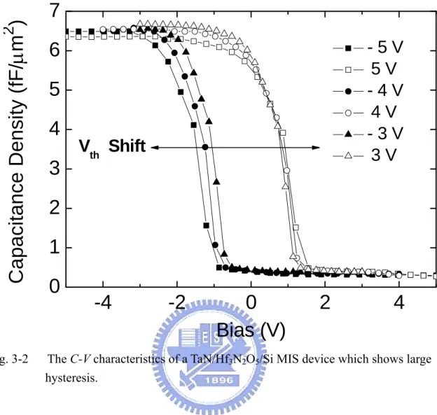
We first determined the N composition in the Hf1-x-yNxOy. Fig. 3-1 shows the XPS spectra of Hf1-x-yNxOy. The existence of Hf, N and O are clear in the XPS spectra, where the composition was determined to be Hf3N2O5. Fig. 3-2 shows the measured C-V characteristics of a high-κ Hf3N2O5 MIS capacitor. We found a large C-V hysteresis of 1.9 to 2.4 V as the sweep voltage was increased from ±3 to ±5 V. This suggests that the charge trapping characteristics of the Hf3N2O5 dielectric are better than those reported for AlN [3.5], and it is likely due to a higher trap density and/or a deeper energy of those traps.
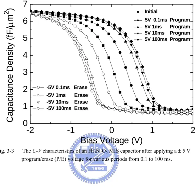
Fig. 3-3 shows the characteristics of a high-κ Hf3N2O5 capacitor after applying +5 or -5V voltage for 0.1 to 100ms. The positive or negative shift of the threshold voltage (Vth), corresponding to a +5 or -5V applied voltage, indicates that the device can be programmed or erased, respectively. These phenomena are similar to non-volatile Flash or SONOS memory[3.1]-[3.4]. The devices showed a capacitance density of 6.5 fF/μm2, which indicate a κ value of ~22 for the Hf3N2O5. The high capacitor density is important for backend capacitor due to the very thick equivalent oxide thickness (EOT). The capacitor density of
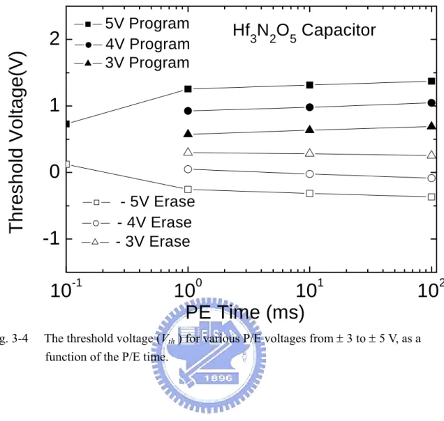
TaN/Hf3N2O5/Si device is also higher than those SONOS capacitors [3.2]-[3.4]. Fig. 3-4 displays the Vth shift as a function of the program/erase time. The⎪Vth⎪ increases with P/E
time, as does ΔVth with increasing P/E voltage. This suggests that the Vth shift mechanism is
caused by charge trapping and indicated the good charge storage. We found a switching speed of ~ 1 ms, due to the rapid increase of Vth between 0.1 to 1 ms and the approximate saturation for times from 1 to 100 ms. From the Vth shift for P/E conditions of ± 5 V for 1ms, a memory window of 1.5 V was measured which is larger than that of an AlN device [3.5] and is comparable with certain SONOS NVM [3.6] data. In addition, the feature of nearly symmetrical positive and negative Vth for program and erase function is important for low voltage applications.
For comparison, we also measured the C-V characteristics of high-κ Si3N4 and Al2O3 capacitors, shown in Fig. 3-5 and Fig. 3-6. For Si3N4 capacitor, only a few mV Vth shift is shown after applying voltages of ± 4 V, which suggests shallower trap energy or lower trap density in the Si3N4. The larger hysteresis of C-V curve indicates the stronger carrier trapping (high density and/or deeper energy of traps) in the Hf3N2O5 device than that of Si3N4 capacitor. For Al2O3 capacitor, Vth increases continuously after applying a negative voltage as high as -8V. Therefore, no erase function is shown, even after applying a higher negative voltage close to device breakdown. It may be due to increasing trapping negative charges in the high-κ dielectrics. The Vth change of Al2O3 capacitors after applying +4V is similar to the
35
hysteresis found in high-κ dielectrics, which is due to dielectric traps. A higher trap density is needed to achieve a higher Vth change, and the C-V shift values are much larger than Si3N4. This result suggests a higher trap density inside the Al2O3 dielectrics compared with Si3N4. This is also the motivation to replace Si3N4 by Al2O3 in MONOS or SONOS memories [3.2] [3.3] [3.7].
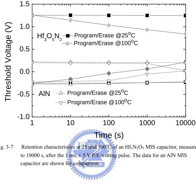
Data retention is one of the most important characteristics for memory applications. Fig. 3-7 shows the retention characteristics of an Hf3N2O5 MIS capacitor at 25 and 100oC, measured after ± 5 V and 1 ms P/E, for periods from 1 to 10000 s. The data of an AlN MIS capacitor are included for comparison. The retention data indicates Program and Erase decay rates of only 2 and 6.2 mV/dec, at 25oC. At 100oC, the decay rates increased to 104 and 116 mV/dec. Such decay rates are still comparable with the 85oC data of advanced SONOS or MONOS NVM [3.2] [3.6] devices. Moreover, the retention of this Hf3N2O5 device is significantly better than that of an AlN MIS capacitor which had a closed memory window at 10000 s at 100oC. Further improvement is required to extend the high temperature retention, although these results are already useful for DRAM improvement.
3.2 Energy barrier and trap energy level
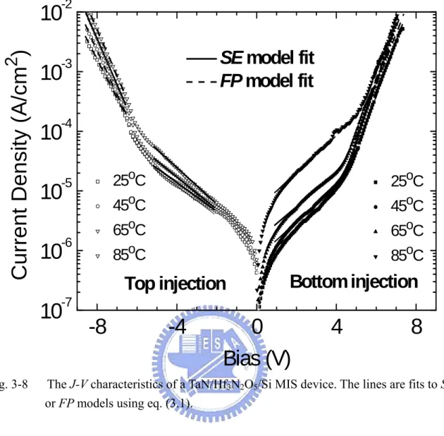
In order to investigate the trap energy, we measured the J-V characteristics. Fig. 3-8 showing measured J-V curves from 25 to 85oC. The J-V characteristics fit theoretical models for Schottky emission (SE) at low electric field and Frankel-Pool (FP) conduction at high voltages [3.8]. The model expression is simply [3.8]:
J ∝ exp[(γE1/2-qϕ
b,t)/kT] , (3.1)
where ϕb orϕt are the Schottky barrier of the metal-electrode/dielectric or the FP trap energy level in the dielectric, respectively. The slope γ can be expressed as:
γ= (q
3/ηπε0κ∞) (3.2)
The constant η has a value 1 or 4 for the FP and SE cases respectively. In (3.2) ε0 is the vacuum permittivity, and κ∞ is the high-frequency dielectric constant (= n2; n being the refractive index).
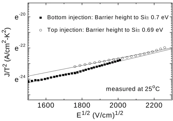
To extract the Schottky barrier ϕb, we have plotted the ln(J/T2)-E1/2 relation [3.8] in Fig.
3-9. A ϕb of 0.70 eV was obtained for the lower Hf3N2O5/Si interface from a fit of eq. (3.1) to the measured ln(J/T2)-E1/2 data. This value is, coincidently, close to the 0.69 eV value
extracted for the upper TaN/Hf3N2O5 interface.
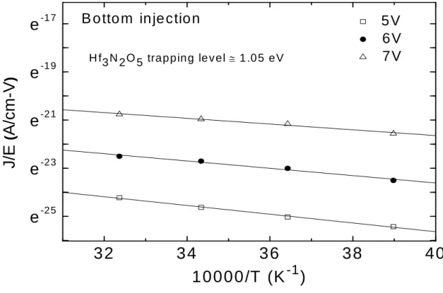
To extract the trap energy, we have plotted the ln(J/E)-1/kT relationship [3.8]in Fig. 3-10. This gives extracted trap energy of 1.05 eV for current injection from the lower Hf3N2O5/Si interface. This value reduces to 1.01 eV for current injection from the top TaN/Hf3N2O5
37
interface, as shown in Fig. 3-11. The slight energy difference may be due to the background moisture and pressure transients at the beginning of reactive sputtering which could result in slightly higher oxygen content in the HfNO.
In Fig. 3-12 we summarize the band diagram of the TaN/Hf3N2O5/Si MIS structure. The barrier height of 0.7 eV is significantly less than that of HfO2 due to the high content nitrogen in the HfNO [3.9]. It is important to notice that the trap energy of Hf3N2O5 is 1.01~1.05 eV
below the conduction band of Hf3N2O5. Such a deep trap energy (within the Si forbidden gap) is vitally important for good data retention due to a lack of allowed states within the Si bandgap – this also explains the large C-V hysteresis shown in Fig. 3-2.
In conclusion, we have fabricated the TaN/Hf3N2O5/Si MIS capacitors which displayed a high capacitance density of ~6.5 fF/μm2 and a large C-V hysteresis necessary for charge storage. Measured J-V characteristics indicated a deep trapping level of 1.01~1.05 eV.
3.3 The applications of MIS capacitors
For analog and RF [3.10]–[3.15] ICs and memory applications, capacitors with a high capacitance density are preferred. It is also desirable to have a program-erasable capability. This is especially important for RF ICs where process variations can shift the resonance frequency of LC tank away from designed values, creating impedance mismatches and bandpass frequency differences [3.16]. In addition, the high-κ Hf3N2O5 capacitor has the high capacitance density of ~6.5fF/μm2. Such a high capacitance density is importance for analog and RF applications [3.17]-[3.20] to reduce the chip size. This capacitance density is 5~6 times larger than capacitors currently provided by IC foundries, and would yield a 5~6 times smaller capacitor area in the circuit of a die.
For one-transistor-one-capacitor (1T1C) volatile memory like DRAM, this high density (6.5fF/μm2) Hf
3N2O5 capacitor can be programmed and erased with voltage of +5V and -5V for ≦ 1m sec. The mechanism for this may be charge trapping or de-trapping in the high-trap-density Hf3N2O5. The retention data decay rates were only 2 and 6.2 mV/dec of program and erase at 25oC. This is already better than volatile DRAM. The charge loss in a DRAM capacitor is a serious issue, where high capacitance density and frequency refreshing is needed around each 1ms, but due to the limited availability of high-k dielectrics this becomes difficult as devices are scale down. As a result, program and erasable capacitors can extend the data retention for DRAM leading to less refreshing cycles.
39
The Hf3N2O5 capacitor has the large C-V hysteresis of 1.9 to 2.4 V as the sweep voltage was increased from ±3 to ±5 V (shown in Fig. 3-2), which is similar to SONOS or MONOS memories. It is already larger than other dielectrics in flash memories due to its deep trapping level of 1.01~1.05 eV. Besides, it also has large dielectric constant κ ~22. So, it is suitable to use Hf3N2O5 as trapping layer in SONOS or MONOS type flash memories.
600
500
400
300
200
100
0
Atomic %
O
1s
49.95
Hf
4f
30.22
N
1s
19.83
Hf
4f
N
1sO
1s
Intensi
ty (a.
u
.)
Binding energy (eV)
Fig. 3-1 XPS spectra of Hf1-x-yNxOy, where composition of Hf3N2O5 was determined from measurement.
41
-4
-2
0
2
4
0
1
2
3
4
5
6
7
Capacitance Density (fF/
μ
m
2
)
Bias (V)
- 5 V
5 V
- 4 V
4 V
- 3 V
3 V
V
thShift
Fig. 3-2 The C-V characteristics of a TaN/Hf3N2O5/Si MIS device which shows large hysteresis.
-2
-1
0
1
2
0
1
2
3
4
5
6
7
-5V 0.1ms Erase -5V 1msErase -5V 10ms Erase -5V 100ms Erase Initial 5V 0.1ms Program 5V 1ms Program 5V 10ms Program 5V 100ms Program
C
a
pacitance D
e
nsity (
fF
/
μ
m
2
)
Bias Voltage (V)
Fig. 3-3 The C-V characteristics of an Hf3N2O5 MIS capacitor after applying a ± 5 V program/erase (P/E) voltage for various periods from 0.1 to 100 ms.
43
10
-110
010
110
2-1
0
1
2
- 3V Erase
- 4V Erase
- 5V Erase
3V Program
4V Program
5V Program
T
h
reshold Voltage(V)
PE Time (ms)
Hf
3N
2O
5Capacitor
Fig. 3-4 The threshold voltage (Vth ) for various P/E voltages from ± 3 to ± 5 V, as a
Fig. 3-5 C-V characteristics of a high-κ Si3N4 capacitor. A small C-V shift was shown after applying of +4V and -4V.
-3
-2
-1
0
1
0
1
2
3
4
Si
3N
4Capacitor
Initial
4V 1ms Program
4V 10ms Program
4V 100ms Program
4V 1ms Erase
4V 10ms Erase
4V 100ms Erase
Capacitance Density (fF/
μ
m
2)
Bias (V)
45
Fig. 3-6 Measured C-V characteristics of a high-κ Al2O3 capacitor. Continuously
increasing Vth is measured even at high negative voltage of -8V but still without erase function.
-2
-1
0
1
2
0
1
2
3
4
5
Continuously increasing V
thAl
2O
3Capacitor
Initial
4V Program
-4V
-6V
-8V
Capacitance density (fF/
μ
m
2)
Bias (V)
1
10
100
1000
10000
-1.0
-0.5
0.0
0.5
1.0
1.5
AlN
Program/Erase @25oC Program/Erase @100oCHf
3O
5N
2Threshold Voltage (V)
Time (s)
Program/Erase @25oC Program/Erase @100oCFig. 3-7 Retention characteristics at 25 and 100oC of an Hf3N2O5 MIS capacitor, measured to 10000 s, after the 1 ms, ± 5 V P/E writing pulse. The data for an AlN MIS capacitor are shown for comparison.
47
-8
-4
0
4
8
10
-710
-610
-510
-410
-310
-2SE model fit
FP model fit
25
oC
45
oC
65
oC
85
oC
25
oC
45
oC
65
oC
85
oC
Top injection
Current Densi
ty (A/cm
2
)
Bias (V)
Bottom injection
Fig. 3-8 The J-V characteristics of a TaN/Hf3N2O5/Si MIS device. The lines are fits to SE or FP models using eq. (3.1).
1600
1800
2000
2200
e
-24e
-22e
-20 Bottom injection: Barrier height to Si≅ 0.7 eV Top injection: Barrier height to Si≅ 0.69 eVmeasured at 25
oC
J/T
2(A/cm
2-K
2)
E
1/2(V/cm)
1/2Fig. 3-9 A ln(J/T2)-E1/2 plot and SE calculations for TaN/Hf3N2O5/Si capacitor data at low electric field with electron injection from either lower Si or upper TaN electrodes.
49
32
34
36
38
40
e
-2 5e
-2 3e
-2 1e
-1 9e
-1 75V
6V
7V
H f3N2O5 trapping level ≅ 1 .0 5 e V
J/E
(
A/cm-V
)
10000/T (K
-1)
B o tto m inje ction
Fig. 3-10 The ln(J/E)-1/kT plots and FP calculations of bottom injection forTaN/Hf3N2O5/Si device data at high field.
32
34
36
38
40
e
-24e
-21e
-186V
7V
8V
Hf3N2O5 trapping level ≅ 1.01 eVJ/E
(
A/cm-V
)
10000/T (K
-1)
Top injection
Fig. 3-11 The ln(J/E)-1/kT plots and FP calculations of top injection for TaN/Hf3N2O5/Si device data at high field.
Fiig. 3-12 B a c d
Band diagra and trap ene calculations data. am of Hf3N ergy were ob s to the mea 51 N2O5 MIS de btained from sured ln(J/T evices. The m SE and F T2)-E1/2 and barrier heig FP model ln(J/E)-1/k ght kT
Chapter 4
Conclusion
We have demonstrated a program-erasable high-κ Hf3N2O5 MIS capacitor for many applications such as DRAM and Flash memories. The programmed charges can be erased by a low operation voltage of -5V for 1ms. The other merits of this capacitors includes good data retention for 104 sec which can extend long memory time, a high capacitance density of ~6.5 fF/μm2 can reduce the chip size, and a large C-V hysteresis necessary for charge storage. So, this program-erasable high-κ Hf3N2O5 capacitor with good data retention would provide an alternative solution to volatile and nonvolatile memories.
We also compared the trapping capability with Si3N4 and Al2O3. Only a small C-V shift was shown in the Si3N4 capacitors which suggest shallower trap energy or lower trap density in that. The measured C-V characteristics of Al2O3 capacitors was observed continuously increasing Vth and could not be erased by negative voltage. It may be due to increasing trapping negative charges in the high-κ dielectrics. At the end of the discussion, we measured J-V characteristics and found a deep trapping level of 1.01~1.05 eV by theoretical models for Schottky emission (SE) at low electric field and Frankel-Pool (FP) conduction at high voltages.
53
high capacitance density of ~6.5 fF/μm2, a large C-V hysteresis, a good data retention property and a deep trapping level of 1.01~1.05 eV.
References
Chapter 1:
[1.1] G. D. Wilk, R. M. Wallace, and J. M. Anthony, “High-κ gate dielectrics: Current status and materials properties considerations,” J. Appl. Phys., Vol. 89, No. 10, 15 May 2001.
[1.2] M. Koyama, K. Suguro, M. Yoshiki, Y. Kamimuta, M. Koike, M. Ohse, C. Hongo and A. Nishiyama, “Thermally stable ultra-thin nitrogen incorporated ZrO2 gate dielectric prepared by low temperature oxidation of ZrN,” in IEDM Tech. Dig., pp. 20.3.1-20.3.4, 2001.
[1.3] E. P. Gusev, D. A. Buchanan, E. Cartier, A. Kumar, D. DiMaria, S. Guha, A. Callegari, S. Zafar, P. C. Jamison, D. A. Neumayer, M. Copel, M. A. Gribelyuk, H. Okorn-Schmidt, C. D Emic, P. Kozlowski, K. Chan, N. Bojarczuk, L. -A. Ragnarsson and Rons, “Ultrathin high-κ gate stacks for advanced CMOS devices,” in IEDM Tech.
Dig., pp. 20.1.1-20.1.4, 2001.
[1.4] W. Zhu, T. P. Ma, T. Tamagawa, Y. Di, J. Kim, R. Carruthers, M. Gibson and T. Furukawa, “HfO2 and HfAlO for CMOS: thermal stability and current transport,” in
IEDM Tech. Dig., pp. 20.4.1-20.4.4, 2001.
[1.5] L. Kang, K. Onishi, Y. Jeon, Byoung Hun Lee, C. Kang, Wen-Jie Qi, R. Nieh, S. Gopalan, R Choi and J. C. Lee, “ MOSFET devices with polysilicon on single-layer HfO2 high-κ dielectrics,” in IEDM Tech. Dig., pp. 35-38, 2000.
55
Dharmarajan and J. C. Lee, “High-quality ultra-thin HfO2 gate dielectric MOSFETs with TaN electrode and nitridation surface preparation,” in IEDM Tech. Dig., pp. 15-16, 2001.
[1.7] Z. J. Luo, T. P. Ma, E. Cartier, M. Copel, T. Tamagawa and B. Halpern, “Ultra-thin ZrO2 (or silicate) with high thermal stability for CMOS gate applications,” in Symp. on
VLSI Technology, pp. 135-136, 2001.
[1.8] International Technology Roadmap for Semiconductor, 2004.
[1.9] G. Shang, P. W. Peacock, and J. Robertson, “Stability and band offsets of nitrogenated high-dielectric-constant gate oxides,” in American Institute of Physics.., pp. 106-108,
2004.
[1.10] T. H. Perng, C. H. Chien, C. W. Chen, M. J. Yang, Peer Lehnen, C. Y. Chang, and T. Y. Huang, “HfO2 MIS capacitor with copper gate electrode,” in IEEE electron device letters, VOL. 24, NO. 4, pp. 784-786, 2004.
[1.11] H. Y. Yu, H. F. Lim, J. H. Chen, M. F. Li, Chunxiang Zhu, C. H. Tung, A. Y. Du, W. D. Wang, D. Z. Chi, and D.-L. Kwong , “Physical and electrical characteristics of HfN gate electrode for advanced MOS devices,” in IEEE electron device letters, VOL. 24, NO. 4, pp. 784-786, 2003.
[1.12] C. Hu, “Gate oxide scaling limits and projection,” in IEDM Tech. Dig., 1996, pp. 319–322.
[1.13] Y. Momiyama, H. Minakata, and T. Sugii, “Ultra-thin Ta2O5 =SiO2 gate insulator with TiN gate technology for 0.1 μm MOSFET’s,” in Symp. VLSI Tech. Dig., 1997, pp.
135–136.
[1.14] D. A. Neumayer and E. Cartier, “Materials characterization of ZrO2–SiO2 and HfO2–SiO2 binary oxides deposited by chemical solution deposition,” in J. Appl. Phys.
90, 1801 (2001).
[1.15] K. Yamamoto, S. Hayashi, M. Kubota, and M. Niwa, “Electrical and physical properties of HfO2 films prepared by remote plasma oxidation of Hf metal,” in Appl.
Phys. Lett. 81,2053 ,(2002).
[1.16] C. S. Kang, H. J. Cho, R. Choi, Y. H. Kim, C. Y. Kang, S. J. Rhee, C.Choi, M. S. Akbar, and J. C. Lee, “The electrical and material characterization of hafnium oxynitride gate dielectrics with TaN-gate electrode,” in IEEE Trans. Electron Devices
51, 220 (2004).
[1.17] C. H. Choi, T. S. Jeon, R. Clark, and D. L. Kwong, “Electrical properties and thermal stability of CVD HfOxNy gate dielectric with poly-Si gate electrode,” in IEEE
Electron Device Lett. 24, 215 (2003).
[1.18] T. Yamaguchi, R. Iijima, T. Ino, A. Nishiyama, H. Satake, and N.Fukushima, “Additional scattering effects for mobility degradation in Hf-silicate gate MISFETs,” in IEDM Tech. Dig., 2002, pp. 621–624.
[1.19] A. L. P. Rotondaro, M. R. Visokay, J. J. Chambers, A. Shanware, R. Khamankar,H. Bu, R. T. Laaksonen, L. Tsung, M. Douglas, R.Kuan, M. J. Bevan, T. Grider, J. McPherson, and L. Colombo, “Advanced CMOS transistors with a novel HfSiON gate dielectric,” in VLSI Tech. Dig., 2002, pp. 11–13.
57
[1.20] J. L. Gavartin, A. L. Shluger, A. S. Foster, and G. I. Bersuker, ” The role of nitrogen-related defects in high-k dielectric oxides: Density-functional studies,” J.
Appl. Phys. 97, 053704 _2005.
[1.21] G. E. Tellison and F. A. Modine, “Parameterization of the optical functions of amorphous materials in the interband region,” in Appl. Phys. Lett. 69, 371 _1996.
[1.22] G. E. Tellison and F. A. Modine, “Parameterization of the optical functions of amorphous materials in the interband region,” in Appl. Phys. Lett. 69, 2137 _1996.
[1.23] C. S. Kang, H. J. Cho, R. Choi, Y. H. Kim, C. Y. Kang, S. J. Rhee, C. Choi, Mohammad Shahariar Akbar, and Jack C. Lee “The electrical and material characterization of hafnium oxynitride gate dielectrics with TaN-gate electrode,” in IEEE transactions on
electron devices, VOL. 51, NO. 2, pp. 220-227, 2004.
[1.24] G. Shang, P. W. Peacock, and J. Robertson, “Stability and band offsets of nitrogenated high-dielectric-constant gate oxides,” in American Institute of Physics ,applied physics letters volume 84, pp. 106-108,2004.
[1.25] S. J. Wanga, J. W. Chai, Y. F. Dong , Y. P. Feng N. Sutanto, J. S. Pan, and A. C. H. Huan, “Effect of nitrogen incorporation on the electronic structure and thermal stability of HfO2 gate dielectric,” in American Institute of Physics ,applied physics letters volume 88, 192103,2006.
[1.26] M. Liu, Q. Fang, G. He, L. Li, L. Q. Zhu, G. H. Li, and L. D. Zhang, “Effect of post deposition annealing on the optical properties of HfOxNy films,” in American Institute of Physics ,applied physics letters volume 88, 192904,2006.
[1.27] J. Choi, R. Puthenkovilakam, and J. P. Chang, “Effect of nitrogen on the electronic properties of hafnium oxynitrides,” in American Institute of Physics ,in J. Appl. Phys. Lett.99, 053705, 2006.
[1.28] C. L. Cheng, K. Shu, C. Liao, C. H. Huang, and T. K. Wang, “Current-conduction and charge trapping properties due to bulk nitrogen in HfOxNy gate dielectric of metal-oxide-semiconductor devices,” in American Institute of Physics ,applied physics letters volume 86, 212902,2005.
[1.29] T. H. Perng, C. H. Chien, C. W. Chen, M. J. Yang, P. Lehnen, C. Y. Chang, and T. Y. Huang, “HfO2 MIS capacitor with copper gate electrode,” in IEEE electron device
letters, VOL. 25, NO. 12, pp. 784-786, 2004.
[1.30] H. Y. Yu, H. F. Lim, J. H. Chen, M. F. Li, Chunxiang Zhu, C. H. Tung, A. Y. Du, W. D. Wang, D. Z. Chi, and D.-L. Kwong, “Physical and Electrical Characteristics of HfN GateElectrode for Advanced MOS Devices,” in IEEE electron device letters, VOL. 24, NO. 4, pp. 230-232, 2003.
[1.31] G. Pant, A. Gnade, M. J. Kim, R. M. Wallace, B. E. Gnade, M. A. Quevedo-Lopez, P. D. Kirsch, and S. Krishnan, “Comparison of electrical and chemical characteristics of ultrathin HfON versus HfSiON dielectrics,” in American Institute of Physics ,applied physics letters volume 89, 032904,2006.
[1.32] Donald A. Neamen “Semiconductor Physics and Devices Basic Principles” 3rd edition McGraw Hill, 2003.
59
[1.33] M. Pecovska-gjorgjevicha, E. Atanassova, N. Novkovski, and D. Spasov “Dielectric characteristics and conduction mechanism of Ta2O5 MOS structures with various gate electrodes” Applied Physics / Poster Presentations,2003.
[1.34] S. M. Sze “Physics of Semiconductor Devices” 2nd edition New York: Wiley, 1981.
[1.35] ”The study of MOS characteristics using rare-earth oxide Y2O3 as gate dielectrics” Submitted to Department of Electronic Engineering Chung Yuan Christian University In Partial Fulfillment of the Requirements for the Degree of Master of Science, 2000.
[1.36] Ben G. Streeman and Sanjay Kumar Banerjee “Solid State Electronic Devices” 6th edition Prentice Hall, 2006.
Chapter 3:
[3.1] M. H. White, D. A. Adams, and J. Bu, “On the go with SONOS,” IEEE Circuits &
Devices Magazine, vol. 16, pp. 22-31, 2000.
[3.2] C. H. Lee, K. I. Choi, M. K. Cho, Y. H. Song, K. C. Park, and K. Kim, “A novel SONOS structure of SiO2/SiN/Al2O3 with TaN metal gate for multi-Giga bit Flash memeries,” in IEDM Tech. Dig., pp. 613-616, 2003.
[3.3] T. Sugizaki, M. Kobayashi, M. Ishidao, H. Minakata, M. Yamaguchi, Y. Tamura, Y. Sugiyama, T. Nakanishi, and H. Tanaka, “Novel multi-bit SONOS type flash memory using a high-κ charge trapping layer,” in Symp. on VLSITech. Dig., pp. 27-28, 2003.
[3.4] A. Chin, C. C. Laio, C. Chen, K. C. Chiang, D. S. Yu, W. J. Yoo, G. S. Samudra, T. Wang, I. J. Hsieh, S. P. McAlister, and C. C. Chi, “Low voltage high speed
SiO2/AlGaN/AlLaO3/TaN memory with good retention,” in IEDM Tech. Dig., pp. 165-168, 2005.
[3.5] C. H. Lai, B. F. Hung, A. Chin, W. J. Yoo, M. F. Li, C. Zhu, S. P. McAlister, and D. L. Kwong, “A novel program-erasable high-κ AlN capacitor,” IEEE Electron Device Lett., vol. 26, pp. 148-150, March 2005.
[3.6] M. Specht, R. Kommling, L. Dreeskornfeld, W. Weber, F. Hofmann, D. Alvarez, J. Kretz, R.J. Luyken, W. Rosner, H. Reisinger, E. Landgraf, T. Schulz, J. Hartwich, M. Stadele, V. Klandievski, E. Hartmann, and L. Risch, “Sub-40nm tri-gate charge trapping nonvolatile memory cells for high-density applications,” in Symp. on VLSI
Tech. Dig., 2004, pp. 244-245.
[3.7] M. Specht, H. Reisinger, M. Stadele, F. Hofmann, A. Gschwandtner, E. Landgraf, R. J. Luyken, T. Schulz, J. Hartwich, L. Dreeskornfeld, W. Rosner, J. Kretz, and L. Risch, “Retention time of novel charge trapping memories using Al2O3 dielectrics,” 33rd European Solid-State Device Research Conf. (ESSDERC), 2003, pp. 16-18.
[3.8] K. C. Chiang, C. C. Huang, G. L. Chen, W. J. Chen, H. L. Kao,Y. H. Wu, Albert Chin, S. P. McAlister, “High-performance SrTiO3 MIM capacitors for analog applications,”
IEEE Trans. Electron Devices, vol. 53, pp. 2312-2319, September 2006.
[3.9] J Robertson, “Band offsets of wide-band-gap oxides and implications for future electronic devices,” J Vac Sci Technol B, vol. 18, pp. 1785-1791, May 2000.
[3.10] S. B. Chen, J. H. Chou, A. Chin, J. C. Hsieh, and J. Liu, “High density MIM capacitors using Al O and AlTiO dielectrics,” IEEE Electron Device Lett., vol. 23, no.
61
[3.11] S. B. Chen, C. H. Lai, A. Chin, J. C. Hsieh, and J. Liu, “RF MIM capacitors using high-K Al O and AlTiO dielectrics,” in Proc. MTT-S Int. Microwave Symp., vol. 1, 2002, pp. 201–204.
[3.12] D. Coolbaugh, E. Eshun, R. Groves, D. Harame, J. Johnson, M.Hammad, Z. He, V. Ramachandran, K. Stein, S. S. Onge, S. Subbanna,D. Wang, R. Volant, X. Wang, and K. Watshon, “Advanced passivedevices for enhanced integrated RF circuit performance,” in Proc.RF-IC Symp., 2002, pp. 341–344.
[3.13] T. Soorapanth, C. P. Yue, D. K. Shaeffer, T. H. Lee, and S. S. Wong,“Analysis and optimization of accumulation-mode varactor for RF ICs,”in Symp. VLSI Circuits Dig., 1998, pp. 32–33.
[3.14] M. Y. Yang, C. H. Huang, A. Chin, C. Zhu, B. J. Cho, M. F. Li, andD. L. Kwong, “Very high density RF MIM capacitors using high-κ Al2O3 doped Ta2O5 dielectrics,”
IEEE Microw. WirelessCompon. Lett., vol. 13, no. 10, pp. 431–433, Oct. 2003.
[3.15] C. Zhu, H. Hu, X. Yu, A. Chin, M. F. Li, and D. L. Kwong, “Voltage temperature dependence of capacitance of high-K HfO MIM capacitors: A unified understanding and prediction,” in IEDM Tech. Dig., 2003, pp.379–382.
[3.16] C. H. Lai, C. F. Lee, A. Chin, C. H.Wu, C. Zhu, M. F. Li, S. P. McAlister, and D. L. Kwong, “A tunable and program-erasable capacitor on Si with long tuning memory,” in Proc. RF-IC Symp. Dig., 2004, pp. 259–262.
[3.17] C. H. Huang, D. S. Yu, A. Chin, W. J. Chen, C. X. Zhu, M.-F. Li, B. J. Cho, and D. L. Kwong, “Fully silicided NiSi and germanided NiGe dual gates on SiO –Si and Al O –Ge-on-insulator MOSFETs,” in IEDM Tech. Dig., 2003, pp. 319–322.
[3.18] C. H. Huang, M. Y. Yang, A. Chin, W. J. Chen, C. X. Zhu, B. J. Cho, M.-F. Li, and D. L. Kwong, “Very low defects and high performance Ge-on-insulator p-MOSFETs with Al O gate dielectrics,” in Symp. VLSI Tech. Dig., 2003, pp. 119–120.
[3.19] H. Iwai, S. Ohmi, S. Akama, C. Ohshima, A. Kikuchi, I. Kashiwagi, J. Taguchi, H. Yamamoto, J. Tonotani, Y. Kim, I. Ueda, A. Kuriyama, and Y. Yoshihara, “Advanced gate dielectric materials for sub-100 nm CMOS,” in IEDM Tech. Dig., 2002, pp. 625–628.
[3.20] A. Chin, Y. H.Wu, S. B. Chen, C. C. Liao, andW. J. Chen, “High quality La O and Al O gate dielectrics with equivalent oxide thickness 5–10 Å,” in Symp. VLSI Tech. Dig., 2000, pp. 16–17.
63
Vita
姓名:林俊賢 性別:男 出生年月日:民國 68 年 12 月 11 日 籍貫:台灣省雲林縣 住址: 雲林縣斗六市建興路 95 號 學歷:國立中興大學物理系 (民國 87 年 9 月~民國 91 年 6 月) 國立交通大學電機學院微電子奈米科技產業研發碩士班 (民國 95 年 2 月~民國 97 年 1 月) 論文題目: 可寫入-抹除高介電常數氮氧化鉿 金屬-絕緣層-矽 電容A Program-Erasable High-κ Hf3N2O5 Metal-Insulator-Silicon Capacitor