國 立 交 通 大 學
電子工程學系 電子研究所碩士班
碩 士 論 文
利用雙重微影成像法製作非對稱 N 型金氧半場效
電晶體之元件特性研究
A Study on the Device Characteristics of
Asymmetric NMOSFETs with Double-Patterning
Technique
研 究 生:簡敏峰
指導教授:林鴻志 博士
黃調元 博士
利用雙重微影成像法製作非對稱 N 型金氧半場效
電晶體之元件特性研究
A Study on the Device Characteristics of
Asymmetric NMOSFETs with Double-patterning
Technique
研 究 生:簡敏峰
Student:Min-Feng Jian
指導教授:林鴻志 博士 Advisors:Dr. Horng-Chih Lin
黃調元 博士
Dr. Tiao-Yuan Huang
國 立 交 通 大 學
電子工程學系 電子研究所碩士班
碩 士 論 文
A Thesis
Submitted to Department of Electronics Engineering & Institute of Electronics College of Electrical and Computer Engineering
National Chiao-Tung University in Partial Fulfillment of the Requirements
for the Degree of Master of Science
in
Electronic Engineering July 2010
Hsinchu, Taiwan, Republic of China
利用雙重微影成像法製作非對稱 N 型金氧半場效
電晶體之元件特性研究
研究生 : 簡敏峰 指導教授 : 林鴻志 博士
黃調元 博士
國立交通大學
電子工程學系 電子研究所碩士班
摘要
在本篇論文中,我們發展出一種新穎的雙重微影成像技術,利用 I 射線光學步 進機,成功製作出 100 奈米閘極圖形的 N 型金氧半場效電晶體。這方法包含了兩 次光學微影,以及蝕刻製程來形成閘極圖形。雖然製程較傳統標準作法複雜,但 可以避免一般製程中的繞射效應,藉此突破 I 射線光學微影方法的解析度極限,達 到 100 奈米甚至更細的線寬。此外,此製程更可以用來製作非對稱的元件。在本 篇論文中,我們調變了非對稱源極/汲極的暈邊(halo)大傾角佈植條件,並分析出大 傾角佈植對於元件基本特性,熱載子退化效應和低頻雜訊所造成的影響。 我們發現大傾角佈植可以有效減少漏電流以及改善短通道效應,可是大傾角 佈植卻會導致更嚴重的逆短通道效應和降低驅動電流。對可靠度而言,由於大傾 角佈植會增加在閘極邊緣下的側向電場強度,進而使熱載子退化效應變得更嚴 重。在非對稱元件運用上,在源極端的大傾角佈植可以改善熱載子可靠度,此現象可歸因於靠近汲極端較小的側向電場.
最後,我們探討大傾角佈植對低頻雜訊之影響。當通道越短時,由於大傾角 佈植會造成臨界電壓不均勻的分佈,故導致低頻雜訊劣化.
A Study on the
Device Characteristics of
Asymmetric NMOSFETs with Double-Patterning
Technique
Student : Min-Feng Jian Advisors : Dr. Horng-Chih Lin
Dr. Tiao-Yuan Huang
Department of Electronics Engineering and Institute of Electronics
National Chiao Tung University, Hsinchu, Taiwan
Abstract
In this thesis, a novel double-patterning technique has been successfully developed and applied to fabricate NMOSFETs with 100 nm gate length using I-line stepper. The method includes twice the lithography and subsequent etching process steps to form the gate patterns. Although more complicated, the approach is useful to lower the impact of diffraction effect on resolution limit. Therefore, this technique has better resolution capability and yields much better control over critical dimension variations that can be achieved by single-patterning. In addition to such capacity in patterning smaller gate length, double-patterning technique is also feasible for fabricating devices with asymmetric halo source/drain (S/D). In this work, we’ve also studied and analyzed the effects of asymmetrical halo implantation on the device characteristics, including hot-electron degradation and low-frequency noise performance.
We found that the halo implantation helps reduce the subthreshold leakage and improves the short channel effects (SCE), but it also causes severe reverse short channel effect (RSCE) and reduces the drive current. For reliability issue, the halo implantation would aggravate the hot-carrier degradation due to an increase in the strength of the lateral electric field under the gate edge in the devices. Using source-side halo devices, the hot carrier immunity is improved as compared to the drain-side halo sample, which is attributed to reduced peak electric field near the drain end.
Finally, we have also investigated the impacts of halo implantation devices on the low frequency noise characteristics. Halo implantation causes non-uniform threshold voltage distribution, resulting in the degradation of low frequency noise in short channel devices.
Acknowledgement
短短 2 年碩士生涯已經過去了,發覺還是有許多東西還是學習不完,不過這一 條道路還是必須走到終點,學生生涯也該畫下一個句點。在這裡要特別感謝兩位指 導教授林鴻志博士和黃調元博士。林鴻志老師讓我學習到做實驗的態度以及如何 分析元件的想法,給予我研究的方向以及面對困難時所應具有得挑戰精神.黃調元 老師的學術上的風範以及層出不窮的故事,都給我茶餘飯後的另類啟發. 在這裡真的要非常謝謝國家奈米實驗室的林家毅研究員,給予我許多研究和 想法上的幫助,也要感謝高頻實驗室的劉汶德工程師,給予我許多學術上的啟發, 令我量測可以達到事半功倍得成效,真得是非常謝謝以上兩位對於這本論文的幫 助。其次要感謝的是 ADTL 的學長們,蔡子儀學長在 NDL 的經驗和功力,真的是 讓我大開眼界,不愧是有 NDL 守護者美稱的強者。在帶領我實驗時,賜與我非常多 的實務經驗,使我的元件能夠順利的產出;在量測時,給予非常多以前的量測經驗, 使我在量測機台上有更深的一層體驗。林哲民學長在元件模擬和理論上也給予我 非常大的幫助,提供寶貴經驗給我吸收茁壯。也要特別謝謝蘇博、徐博、大師, 不吝分享量測上的經驗。也不能忘記感謝林政頤(毛毛)學長、郭嘉豪(maca)學長在 量測以及做實驗時的大力幫助,以及一同去吃飯的快樂(大誤)。另外也不能忘記前 一屆學長張格綸和謝瑞桀學長,在你們的帶領下,我很高興可以加入你們的 MOS 家族。特別五體投地感謝同屆其餘的六位同學:羅正瑋(真.白 toro)、林庭輔(輔神)、 許家維(Rush)、陳冠智、劉禹伶、陳冠宇,兩年多能和你們相處真得是非常快樂也 學習到許多事情。尤其是輔神和真.白 toro,輔神給予許多精神上的鼓勵以及許多 借鏡之處,真.白 toro 則是在論文寫作上給予許多幫助,能夠與你們六位戰友同 甘苦到最後,心情真的是非常爽。 也感謝之前的同學支持,阿原、阿吉、taco、宅宅和王媽,謝謝你們不定期在 MSN 和網誌上噓寒問暖使我能度過這個煉獄般的試驗,給予我試驗的力量。最後 要感謝的是我的父母和妹妹,你們默默關心和支持,是我完成這一份論文不可或 缺的力量。而要感謝的人太多了,最後我想就謝天吧...以及謝謝許多幫助我的人!!! 簡 敏 峰 誌于風城交大 2010 年 7 月Contents
Abstract (Chinese)………... i
Abstract (English)………... iii
Acknowledgement (Chinese)……….. v
Contents ………... vi
Figure Captions………... viii
Table Captions ……….... xiii
Chapter 1 Introduction………...
11.1 General Background and Motivation………. 1
1.1.1 Introduction……….. 1
1.1.2 Double Patterning Technique………... 1
1.2 Asymmetric Halo NMOSFET………... 3
1.3 Motivation ……….. 5
1.4 Organization of the Thesis ………. 5
Chapter 2 Device Fabrication and Measurement Setup………..
62.1 Double Patterning Technique ………. 6
2.2 Devices Fabrication and Process Flow………... 7
2.3 Measurement Setup…. ………... 9
2.3.1 Electrical Measurement Setup……….. 9
2.3.2 Hot Carrier Reliability Measurement Setup………. 9
Chapter 3 Result and Discussion ……….. 13
3.1 Electrical Characteristics of Asymmetric Halo Devices….……… 13 3.1.1 Electrical Characteristics of Symmetric NMOSFETs………. 13 3.1.2 Electrical Characteristics of NMOSFETs with Asymmetrical Halo……… 15 3.2 Hot Carrier Degradation of Asymmetric Halo devices………... 16 3.2.1 Hot Carrier Stress………. 16 3.2.2 Analyses of the Lateral Distribution of Interface Trap Density…………... 18 3.3 Low-Frequency Noise on the Asymmetric Halo NMOSFETs……… 20Chapter 4 Conclusion and Future Work………... 24
4.1 Summary and Conclusion………... 4.2 Future Work………... 24 26 References ……… Figures………... 27 32 Vita……… 66Figure Captions
Chapter 1
Fig. 1.1. Transistor cost and scaling trend of channel length versus years for technology node [2]. ... 32
Fig. 1.2. Components of leakage current mechanism of transistors. ... 32 Fig. 1.3. Position of Halo channel doping. ... 33
Chapter 2
Fig. 2.1. Design of the double patterning masks. Practical gate structure and dimensions (including gate length) are determined by the overlap region of the two masks ... 34 Fig. 2.2. In-line SEM image of a patterned poly-Si line with nominal line width of 100nm. The measured line width in this case is 93 nm ... 35 Fig. 2.3. SEM image of an NMOSFET with nominal length Lmask = 0.1 μm. Practical length was measured to be 118 nm ... 35 Fig. 2.4. In-line SEM image of patterned poly-Si lines located at four different dies of a wafer (marked in red in the inset) with nominal line width of 100 nm. The measured line width in this case ranges from 91 to 124 nm ... 36 Fig. 2.5. The gate length extracted by In-line SEM images as a function of the designed gate length (Lmask). The error bar indicates the standard derivation of the measured data ... 37 Fig. 2.6. CD variations of two lithography technologies with the I-line stepper ... 37 Fig. 2.7. Illustration of fabrication flow: ... 38
(a) formation of LOCOS isolation; (b) poly-gate deposition; (c) G1 mask definition and (optional) source-side halo implantation; (d) G2 mask definition and (optional) drain-side halo implantation; (e) extension implantation; (f) deep S/D implantation; ... 38 Fig. 2.8. Cross-sections of the four splits of fabricated devices. (a) Control sample (Control). (b) Device with source-side halo (S-halo). (c) Device with drain-side halo (D-halo). (d) Device with symmetric S/D halo (S/D-halo) .... 40 Fig. 2.9. Basic setup structure for charge pumping measurements ... 41 Fig. 2.10. Schematic illustrations for the charge pumping measurements with (a) fixed amplitude, (b) fixed base sweep, and (c) fixed peak sweep. The arrows indicate the sweep directions ... 41 Fig. 2.11. Measurement setup of single-junction charge pumping measurement ... 42
Chapter 3
Fig. 3.1. Transfer characteristics of Control with various channel length ranging from 0.1 to 10 μm. All devices have the same width of 10 μm. (a) VD = 0.05 V. (b)
VD = 1.5 V. ... 43
Fig. 3.2. Schematic diagram of the charge sharing model [13] ... 44 Fig. 3.3. Schematic diagram of depletion regions at a high drain bias for Control devices ... 44 Fig. 3.4. 2D electric potential (left) and surface potential versus lateral distance (right) in Control device. Here we defined the vertical direction channel is X-axis and the horizontal direction channel is Y-axis ... 45 Fig. 3.5. Subthreshold characteristics of Control and S/D-halo NMOSFETs with channel width/length = 10 μm / 0.1 μm ... 46
Fig. 3.6. Schematic diagram of depletion regions at a high drain bias for S/D-halo devices ... 46 Fig. 3.7. Threshold voltage as a function of channel length for Control and S/D-halo samples ... 47 Fig. 3.8. Drain induced barrier lowering (DIBL) for Control and S/D-halo NMOSFETs as a function of channel length ... 47 Fig. 3.9. Substreshold swing for Control and S/D-halo NMOSFETs as a function of channel length ... 48 Fig. 3.10. Off-current versus on-current for the Control and the S/D-halo devices ... 48 Fig. 3.11. Diagram showing the non-uniform threshold voltage along the channel with halo implant [22] ... 49 Fig. 3.13. Schematic diagram of depletion region in D-halo devices at a high drain bias
... 50 Fig. 3.14. Schematic diagram of depletion region in S-halo devices at a high drain bias
... 50 Fig. 3.15. Drain induced barrier lowering (DIBL) for all splits of NMOSFETs as a function of channel length ... 51 Fig. 3.16. Substreshold swing for all splits of NMOSFETs as a function of channel length…….. ... 51
Fig. 3.19. Substrate current characteristics and (b) the ratio of substrate current to drain as a function of gate voltage at the given drain bias VD = 3 V ... 53
Fig. 3.20. Subthreshold characteristics and transconductance of devices before and after 3000 sec of hot-electron stressing. Channel length/width = 0.14 m/10 m.(a) Control. (b) S/D-halo. (c) D-halo. (D) S-halo ... 55 Fig. 3.21.Results of (a) threshold voltage shift, (b) interface trap density increase, and (c)
stress time. The hot-electron stressing was performed at VDS = 3 V and VGS at
maximum substrate current. Channel length/width = 0.14 m/10 m ... 57 Fig. 3.22. The increase in charge pumping current after 3000 second of hot carrier stress (VG@Isubmax and VDS = 3 V) for all splits of devices with channel
width/length= 10 m/0.14 m ... 58 Fig. 3.23. Non-uniform distribution of local threshold voltage and flat-band voltage across the device caused by variation of lateral doping concentration. (x=0 is at the drain junction and direct to source junction) ... 58 Fig. 3.24. Derivation of the relationship between local threshold voltage and lateral distance x from the single-junction charge pumping data of the control device ... 59 Fig. 3.25. Extracted lateral profile of local threshold voltage near the graded drain junction in the control sample ... 59 Fig. 3.26. Charge pumping current before and after 1000 second of hot-electron stressing (VG@Isubmax and VDS = 3 V). Channel width/length = 10 m/0.14
m ... 60 Fig. 3.28. Drain current spectrum density (Sid) for the Control and S/D-halo devices with gate length = 0.2 μm showing the 1/fγ spectrum with γ close to one ... 61 Fig. 3.29. Normalized current noise spectral density Sid/Id2 and (gm/Id)2 versus Id for (a)
Control and (b) S/D-halo devices ... 62 Fig. 3.30. Normalized noise power spectrum density versus gate overdrive voltage (Vg–Vt) for Control and S/D-halo devices. The noise measured in the linear
regime. (a) Channel gate length/width = 0.2/10 μm. (b) Channel gate length/width = 10/10 μm ... 63 Fig. 3.31. Normalized noise power spectrum density versus gate overdrive voltage (Vg–Vt) for all splits of devices. Channel gate length/width = 0.2/10 μm .. …64
Fig. 3.32. Normalized noise power spectrum density versus gate overdrive voltage (Vg–Vt) for D-halo and S-halo devices under forward and reverse modes of
operation, respectively ... 64 Fig. 3.33. Normalized noise power spectrum density versus gate overdrive voltage (Vg–Vt) for all splits of devices. Channel gate length/width = 10 μm/10 μm
Table Captions
Table 2.1 Split condition of asymmetric halo structure with double patterning process.. ... 12 Table 2.2 Other implantation conditions used in the NMOS fabrication ... 12
Chapter 1
Introduction
1.1 General Background and Motivation
1.1.1 Introduction
With rapid progress made in manufacturing technology, advance in microelectronics has greatly boosted the function and performance of 3C products in the past decades. For semiconductor industry, the most important thing is to keep improving the chip performance. This mainly depends on the scaling of transistors, and the fundamental principle behind the trend is Moore’s law [1-2]. In 1965, Dr. Moore pointed out that the number of transistors integrated in a chip would increase twice every two year. Although practically the period for two-fold increase in transistor number is not precisely two years, Moore’s law still plays the important role of driver for reducing the cost per transistor and advancing the integrated circuits (IC) revolutions. Figure 1.1 shows the historical trends of transistor cost and feature size for CMOS during the past three decades [3].
Some issues have been discovered when the size of device approaches the physical limitation, including short channel effects, leakage issues, dopant fluctuation, power consumption, reliability issue, parasitic effects such as gate and S/D resistance, parasitic capacitance of junction, and so on. The problems will degrade the characteristics of the next-generation MOSFETs if not handled appropriately. How to improve the performance of MOSFET’s is thus a major concern for the semiconductor industry.
1.1.2 Double Patterning Technique
the goal. In order to reach higher resolution for the feature size reduction, lithographic techniques rely basically on the modulation of three variables of the Rayleigh criterion [4]:
R K NA
1 , (1.1) where λ is the wavelength of the light, NA is numerical aperture, and k1 is a system
constant. Many lithography technologies are developed for the reduction in pattern size, such as immersion technology, off-axis illumination (OAI), the use of phase shift mask (PSM), optical proximity correction (OPC), and extreme ultraviolet lithography (EUVL) [5]. We can improve resolution thanks to the use of shorter wave length, reduced k1 factor, and/or increased NA, as implicated in Rayleigh’s equation. To this
date semiconductor industry has adopted lithography tools with different wavelength of the light sources, like I-line (365 nm), KrF (248 nm) and excimer laser (193 nm) to delineate small dimension. Of course there is no free lunch, the realization of a finer resolution is accompanied with a higher price. Although DUV tools (KrF and ArF) play a dominant role in industry during the past decade, the expensive cost is not affordable for most laboratories in universities. As a result, people in academic field participating in the study of nanotechnology need to find alternative techniques, such as e-beam, ion-beam and I-line lithography systems, for patterning nano-scale dimensions. For e-beam and ion-beam tools which have high resolution capability, the throughput is low. Conventional I-line steppers have much higher throughput and reproducibility but the resolution is limited [6].
The International Technology Roadmap for Semiconductors (ITRS) predicts double patterning for extending lithography process to 45 nm node and beyond by reduction of k1 factor [7-8]. In this work, we adopt this method and incorporate it into
consists of doubling lithography and etch steps. In this study, we use mask 1 to define the left edge of a poly-Si gate. After etching step, we use mask 2 to define the right edge of the gate and complete the gate structure by the following etch step. Because two sides of the gate are defined separately in two different steps, the diffraction effect unavoidable in conventional single patterning process can be promptly lifted, and thus a higher resolution is achievable. Although the increase in mask count and process steps increases the process cost and complexity over the single exposure, the proposed scheme actually provides additional flexibility in device design for optimizing the devices characteristics as asymmetric source/drain can be implemented in the device fabrication.
1.2 Asymmetric Halo NMOSFET
The scaling of MOSFET encounters a number of challenges, such as increased off-state leakage current and short channel effects, including the threshold voltage (VT)
roll-off, the drain induced barrier lowering (DIBL). ICs made of scaled devices require lower power supply levels to reduce power consumption, but it also requires a concomitant reduction in the threshold voltage for drive current boosting. However, a large off-state leakage (IOFF) is also resulted with such evolution due to the limitation
of non-scaleable subthreshold swing (SS).
As described in [9-11] and illustrated in Fig. 1.2 are the leakage current components in an MOSFET. When gate voltage is below threshold voltage and in weak inversion, the diffusion current dominates in the subthreshold region. Note that the depletion region at drain junction widens with increasing drain voltage. In the long-channel case, the penetration of the drain depletion region into the channel would not affect the potential barrier even as the drain bias is large. As the channel
length is short and comparable to the width of drain depletion region, however, the barrier height in the channel for minority carriers to surmount would be reduced by the drain depletion region when the drain bias is increased, leading to a reduction in VT and an increase in subthreshold leakage. This effect is called drain-induced barrier
lowering (DIBL). Since it happens in the surface conduction channel, SS is not affected by the drain bias. However, when the drain bias is further increased, bulk punchthrough between the source and drain occurs, and dramatic increase in SS and subthreshold current are resulted. In order to reduce the leakage currents and keep good control over short channel effect, several channel profile designs have been proposed [12], including super steep retrograde (SSR), channel profile halo (pocket) MOSFET [13], ultra shallow LDD junction device [14], and elevated source/drain process. For the scheme implementing halo structure, halo doping regions are formed locally underneath the source/drain extensions, as shown in Fig. 1.3. For n-channel MOSFET, p-type halo regions are introduced with concentration much higher than the substrate doping concentration. Such design can reduce the penetration of the electric field from the drain and thus prevent the occurrence of punchthrough. The reduction of interaction of the drain junction depletion regime can also help improve DIBL, it is thus a feasible approach for improving the control over the short channel effects. However, too high a halo doping could bring about significant band-to-band tunneling. Sometimes the use of halo doping would cause the reverse short channel effect, and the increment of Vth leads to a reduction in driving current.
Standard CMOS process employs symmetrical S/D structure, so does the halo doping. However, the asymmetric halo structure may benefit the device performance in some respects and have been proposed in a number of papers [15-20]. For example, utilizing source-only halo doping structure can reduce the capacitance of n+p junction
at the drain junction. Better reliability and short-channel effect control are also expected by carefully tailoring the asymmetric S/D and halo structures.
1.3 Motivation
In this work, a novel double patterning technique is proposed and developed to decrease gate dimension down to 100 nm with an I-line stepper. Although the process becomes more complicated over conventional single patterning scheme, the feature size of fabricated device can be significantly reduced. Moreover, the throughput is still much faster than that of e-beam method. The double patterning feature also allows us to separate from the source and drain halo structures. Taking this advantage we can explore and understand the impact of asymmetrical S/D halo on device characteristics.
1.4 Organization of the Thesis
In Chapter 2, we present the process flow utilizing double patterning technique for the fabrication of the NMOS devices with channel length down to 100 nm. We also present the characterization methods and measurement setups in this chapter.
In Chapter 3, characteristics of the fabricated devices are presented and discussed. Special focus is paid on the effects of asymmetric source/drain halo structure on devices’ short-channel behaviors, hot-carrier reliability and low-frequency noise.
Finally, important conclusions generated from our experimental results, discussion and analysis are summarized in Chapter 4.
Chapter 2
Device Fabrication and Measurement Setup
2.1 Double Patterning Technique
A double patterning (DP) technique using twice I-line lithographic process and
subsequent etching step has been developed and demonstrated to achieve 100 nm structure in our study. The two lithographic steps were performed with two different masks. Design of the two masks is shown in Fig. 2.1. The function of G1 mask is to protect the right side of active region to be covered with poly-Si during the subsequent (first) etching process, while the G2 mask protects the left side of the active region and covers portion of poly-Si region remained after the first etching. The overlapped region of the two masks defines the gate length. Although the process is more complicated than conventional one mask process, fine resolution down to 100 nm or even finer can be achieved with the proposed method, far beyond the capability of conventional I-line lithographic technique.
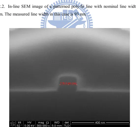
Figure 2.2 shows the in-line SEM images of a poly-Si line pattern formed with the above approach. In this thesis, Lmask represents the designed length on the mask, and Lgate is the practical value measured with In-line SEM. In Fig. 2.2, Lmask and
Lgate are 100 and 93 nm, respectively. Figure 2.3 shows the profile of an etched
poly-Si line with the focused ion beam (FIB) SEM. In this case Lmask and Lgate are 100 and 118 nm, respectively. The above results indicate that variation in the dimension of the gate patterns exists. In order to investigate the phenomenon we check the dimension of line patterns of different dies distributed on a wafer with the In-line SEM. Figure 2.4 shows the results of line patterns with Lmask of 100 nm measured from four dies located at corners of a wafer and the measured dimension
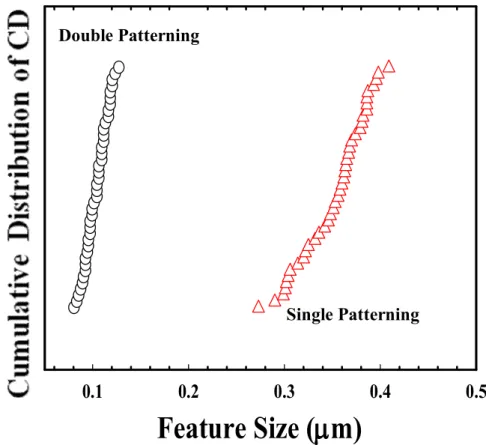
ranges from 91 to 124 nm. The measured results are shown in Fig. 2.5 to check the controllability of critical dimension (CD). The fluctuation of gate length is small as length is larger than 0.3 μm. The results indicate the double patterning technique is feasible to print lines with patterns down to 100 nm, far beyond the resolution limit (~350 nm) of single patterning technique with I-line stepper. However, the fluctuation in the CD of the fine patterns indicates the resolution of this method is mainly limited by the overlay of the stepper. According to the manual provided by the NDL, the overlay accuracy is about 45 nm. Nonetheless, the DP technique actually exhibits tighter CD control than the conventional single patterning one. This merit can be understood with the results shown in Fig. 2.6, in which the variation of CD for DP patterns with Lmask of 100 nm and patterns formed with conventional way with Lmask of 350 nm are compared. These results confirm the feasibility of the proposed DP technique for fabrication of devices with much reduced feature size.
Actually we’ve also designed patterns with Lmask smaller than 80 nm, but we found the results are erratic and difficult to reproduce line patterns with tight dimension distribution. In this thesis we thus focus on fabricating devices with channel length equal or larger than 100 nm. Moreover, with the DP technique, effects of asymmetric halo on device characteristics can be studied.
2.2 Device Fabrication and Process Flow
Figure 2.7 illustrates the fabrication flow of NMOSFETs with basic process steps carried out in our experiment. All the devices were fabricated on 6-inch p-type (100) Si wafers with resistivity of 15~25 Ω-cm and wafer thickness of 655 ~ 695 μm. First the p well was formed by BF2+ implantation at 70 keV with dose of 1×1013 cm-2 and
oxidation of silicon (LOCOS) process with channel stop implant (by BF2+
implantation at 120 keV with dose of 4×1013 cm-2) was used for device isolation. Threshold voltage adjustment and anti-punch through implantation were done by implanting 40 keV BF2+ and 35 keV B+, respectively. When the LOCOS process was
done, 3 nm-thick thermal gate oxide grown in N2O ambient and a 150 nm in situ n+
doped poly-Si layer deposited by low-pressure chemical vapor deposition (LPCVD) were formed on wafer surface.
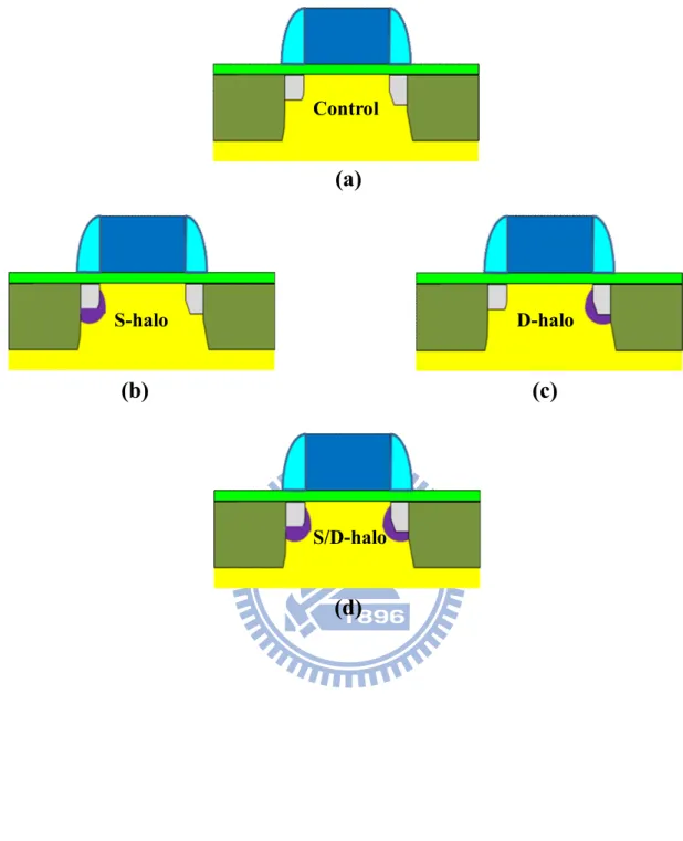
Details about the halo and source/drain (S/D) implantation conditions are shown in Table 2.1. The other implantation conditions used in the fabrication were shown in Table 2.2. For one set of devices, an optional halo implant was done after the gate-1 process, as shown in Fig. 2.7(c) (denoted as S-halo in Table 2.1). In this case the halo is located at the sources side. In contrast, D-halo device listed in Table 2.1 having a drain-side halo received an optional halo implant which was done after gate-2 process as shown in Fig. 2.7(d).It should be noted in this case that, during the halo implant, the PR remained in place to block the source side. We’ve also fabricated devices with symmetric halo, denoted as S/D-halo in Table 2.1, which have the halo formed by stripping off the PR after gate-2 process. The control or Control samples skipped the halo implants mentioned above. For all splits of devices, the S/D extension regions were formed by As+ implantation at 10 keV with dose of 1×1015 cm-2 (Fig. 2.7(e)). Afterwards, a 100 nm TEOS spacer was formed, followed by the formation of S/D regions by As+ implantation at 15 keV with dose of 5×1015 cm-2 (Fig. 2.7(f)). Then the substrate contact region was patterned through lithography and etching processes, followed by a BF2+ implantation at 40 keV with dose of 5×1015 cm-2. Rapid thermal
anneal (RTA) was subsequently carried out in a nitrogen ambient at 1000 C for 10 second to activate dopants in the gate, S/D, and substrate contact regions. After a
standard procedure to form the surface passivation (Fig. 2.7(g)) and contact pads (Fig. 2.7(h)), the wafers received a forming gas anneal performed at 400 C for 30 min. Cross-sectional views of the four splits of test structures are shown in Fig. 2.8.
2.3 Measurement Setup
2.3.1 Electrical Measurement Setup
Electrical measurements of all devices were evaluated by an HP4156A precision semiconductor parameter analyzer and an HP4284 LCR meter. The measurement systems were applied separately to gauge the current-voltage (I-V) and capacitance-voltage (C-V) characteristics. Temperature-regulated hot chucks were used to maintain the measurement temperature at 25 C
2.3.2 Hot Carrier Reliability Measurement Setup
In our study, we’ve performed the hot carrier reliability test to evaluate the performance of the asymmetric halo structures. Hot carrier generation is a strong function of the biasing voltage and the channel length of devices. To ensure small fluctuation in device characteristics so that the validity of test results was not seriously affected, we choose the devices with channel length of 0.14 μm for the testing which were stressed with the drain voltage set at a moderate positive voltage and the gate voltage at which maximum absolute value of substrate current (Isub)
occurred. This was determined by first measuring the Isub -VG characteristics with
moderate positive drain voltage. To monitor the hot-carrier induced degradation, both the ID-VG characteristics at VDS = 0.05 V (linear region) and charge pumping current
were measured before and after the stress. The degradations in terms of threshold voltage shift (Vth), generation of interface trap density (Nit) were recorded and
analyzed in the accelerated stress test.
2.3.3 Charge Pumping Measurement
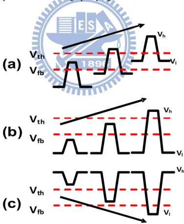
For better understanding the damage mechanism of hot-carrier stress, it is desirable to plot the distribution of both generated interface states and trapped charges. Charge pumping measurement is widely used to characterize the interface state density in MOSFET devices [21]. This type of measurement is very effective because it allows the exclusion of gate leakage contribution to the calculated interface state densities presented in thin gate oxides and at lower frequencies [22-23]. Therefore, to accurately analyze interface state densities or bulk traps in the dielectrics from charge pumping measurement results, we need to pay close attention to the extra leakage current issue. The basic charge pumping measurement includes the measurement of the substrate current while a series of voltage pulses with fixed amplitude, rise time, fall time, frequency, and duty cycle is being applied to the gate of the transistor (Figure 2.9), with source and drain connected to a small reverse bias, and substrate connected to ground. Three conventional types of the voltage pulse train applied to the gate electrode are depicted in Fig. 2.10, namely, (a) fixed amplitude sweep, (b) fixed base sweep, and (c) fixed peak sweep. In this thesis, “fixed amplitude sweep” is used to calculate interface trap density, and “fixed base sweep” is used to analyze the lateral distribution of interface trap, respectively. Square-wave waveforms (f = 1 MHz) were applied to the gate, and the base voltage was varied while keeping the pulse amplitude at 1.5 V to modulate the surface condition from inversion to accumulation. An MOSFET with gate area of AG gives the charge pumping current (Icp) as [24]:
Icp qA fNG it , (2.1)
which the interface trap density (Nit) could be calculated as Icp is measured. The
extracted and discussed in this work. This method is built up with the work of C. Chen et al. [25], and the measurement setup is shown in Fig. 2.10. The measurement procedures are described below:
(1) Measure the Icp-Vh (Vh is the high level of the pulsed voltage train applied to the
gate, see Fig. 2.10) curve on a virgin MOSFET from the drain junction (with the source junction floating), thereby establishing the Vh versus Vth(x) relationship
near the junction of interest [26].
(2) Record the Icp-Vh characteristics after hot-carrier stress.
(3) The hot-carrier-induced interface state distribution, Nit(x), is obtained from the
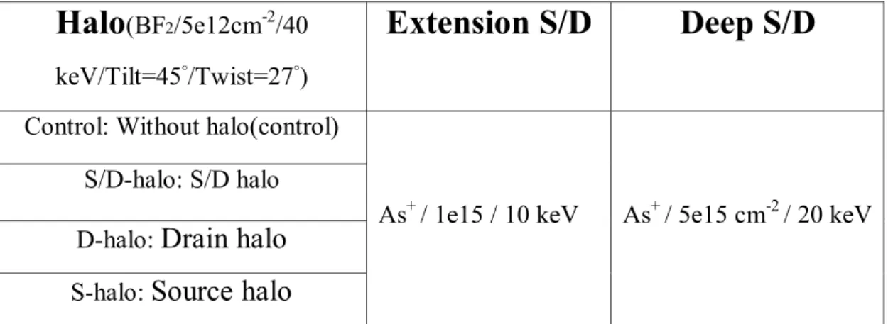
Table 2.1 Split condition of asymmetric halo structure with double patterning process.
Table 2.2 Other implantation conditions used in the NMOS fabrication.
Halo
(BF2/5e12cm-2/40keV/Tilt=45°/Twist=27°)
Extension S/D
Deep S/D
Control: Without halo(control)
As+ / 1e15 / 10 keV As+ / 5e15 cm-2 / 20 keV S/D-halo: S/D halo
D-halo:
Drain halo
S-halo:
Source halo
Conditions Ion Dose / Energy
P-well BF2 1e13 cm-2 / 70 keV
Channel Stop BF2 4e13 cm-2/ 120 keV
Vth BF2 1e13 cm-2/ 40 keV
APT B+ 5e12 cm-2 / 35 keV
Chapter 3
Results and Discussion
3.1 Electrical Characteristics of Asymmetric Halo Devices
3.1.1 Electrical Characteristics of Symmetric NMOSFETs
Above all, this work is to discuss the impacts of halo formation and its location on the performance of NMOSFETs. For the readers’ convenience, we name all splits of test samples as follows: Control represents the control split without halo, S/D-halo represents the control split with symmetric halo, D-halo represents the control split with the drain-side halo, and S-halo represents as control split with the source-side halo. Figure 2.8 shows all splits with different structure.
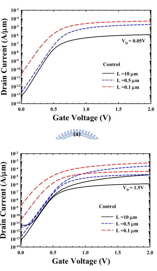
Figure 3.1(a) and Figure 3.1(b) show the transfer characteristics of Control devices with various channel length under different drain bias. As the channel length scales down to 0.1 μm, the flow of bulk punchthrough current becomes obvious and results in degradation of subthreshold characteristics in Control samples. Here we used charging sharing model (Yau, 1974) to illustrate the sharing of the charges in the channel depletion region with the source and drain (S/D) junctions, as shown in Fig. 3.2. In a long channel device, drain and source are so distant that their depletion regions have negligible effects on the potential distribution in the channel. As the channel is sufficiently short and comparable to the width of channel depletion region along the horizontal direction, the portion of charge sharing with S/D junctions becomes significant, resulting in Vth lowering. When a high drain bias is applied to the
short-channel device, the depletion region of the drain junction further penetrates into the channel. This may lead to lowering of potential barrier height at channel surface, as shown in Fig. 3.3 and Fig. 3.4. It indicates that the gate controllability weakens
when the gate length becomes smaller.
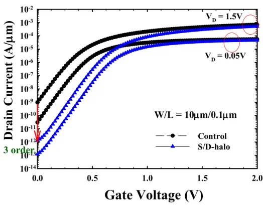
Figure 3.5 shows and compares the subthrehold characteristics for Control and S/D-halo (with symmetrical halo) devices with channel length of 0.1 μm. As can be seen in the figure, the implementation of halo steepens the subthreshold characteristics while the off-state leakage current is reduced by three orders in magnitude due to improved subthreshold swing (SS) and increased threshold voltage (Vth). We can use the illustrations in Fig. 3.4 and Fig. 3.6 to explain the observed
difference revealed in Fig. 3.5. The implementation of halo tends to increase the substrate doping concentration therein and thus reduces the depletion width at channel edges, as shown Fig. 3.6. Furthermore, the lowering in surface potential barrier height with a higher drain voltage is also relieved.
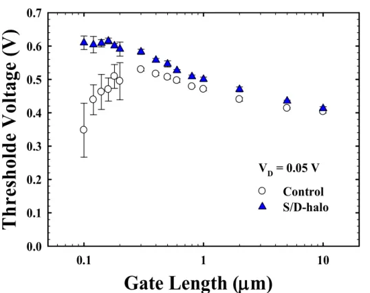
The measured threshold voltages at VDS = 0.05 V as a function of channel length
for the two types of devices are shown in Fig. 3.7. The threshold voltage is defined as the gate voltage at drain current of (W/L).10nA, where L is the channel length and W is the channel width. We note that the two types of devices depict reverse-short-channel-effect (RSCE) which is much severe for S/D-halo. This is reasonable since halo increases doping distribution near the edge of the channel and results in a higher Vth locally. Figure 3.8 shows the drain-induced-barrier-lowering
(DIBL) effect. It is clearly seen that the halo structure reduce DIBL significantly. Subthrehold swing is another guide for evaluating the short-channel effects. The results are shown in Fig 3.9. It appears that devices with halo indeed improve short channel effects. Nevertheless, the halo may degrade the drain current. Figure 3.10 shows that the on-current of the halo devices is much smaller than devices without halo. In the figure it also appears that off-current distribution in Control is wider than S/D-halo, indicating that the halo can help suppress the fluctuation in device characteristics.
3.1.2 Electrical Characteristics of NMOSFETs with Asymmetrical
As demonstrated in previous section, halo implantation effectively improves the
SCEs in MOSFETs. However, it has some drawbacks, such as the drain-substrate coupling, the degradation of driving current and enhanced RSCE. Recently some new MOSFET structures were proposed, such as single halo [27-29], which reduced the problems by eliminating the halo implantation. In order to explain the enhanced threshold voltage variation with the halo implant, a schematic illustration is shown in Fig. 3.11, in which the channel is divided into three regions, including the two halo implant regions near the drain and source with threshold voltage value of Vt1 in the
source junction and Vt3 in the drain junction, respectively. The rest of the channel
without halo is with Vt2, which is smaller than that in the halo region.
To examine the effect of asymmetrical halo structure, we further characterize the D-halo and S-halo devices fabricated in this study. Threshold voltage roll-off characteristics of all splits of devices are shown in Fig. 3.12. We note that, as channel length scales down to 0.1 μm, threshold voltage of the D-halo device (drain-side- halo) is slightly larger than S-halo device (source-side halo), but smaller than that of S/D-halo device (symmetrical halo). Such trend is reasonable when considering the charge sharing model shown in Fig. 3.2. Note in Fig. 3.12, the applied VDS is small
(0.05 V) but not zero, thus the width of depletion region at drain junction is slightly thicker than that at source junction, thus the Vth increase for D-halo is also more
significant.
Figure 3.13 and Fig. 3.14 show the DIBL effect and SS as a function of channel length for different splits. From the figures we can see that the S/D-halo devices exhibit the best performance in suppressing the SCEs, although the D-halo devices show comparable effectiveness. Since the SCEs are closely related to the penetration
of electric field from the edge, especially that originating from the drain with a non-zero drain bias, the D-halo split with drain halo should have better immunity than S-halo devices. We use Fig. 3.15 and Fig. 3.16 to illustrate the depletion width of drain junction. The D-halo has a smaller drain depletion width, thus a smaller charge sharing and less field penetration from the drain as channel length is reduced, resulting in less Vth roll-off and DIBL.
Figure 3.17 shows that the on-current of all splits. Asymmetric halo devices show better on-current than symmetric halo device. On the other hand, symmetric halo device shows reduced off-current as shown in Fig. 3.18. However, this is mainly caused by the severe RSCE (Fig. 3.7) which increases the threshold voltage significantly.
3.2 Hot Carrier Degradation of Asymmetric Halo Devices
3.2.1 Hot Carrier Stress
Mechanisms of hot-carrier induced degradation in MOS devices are strongly related to the impact ionization in the high electric-field region near the drain junction [30-31]. For NMOSFET devices, these generated electrons and holes during impact ionization process are separately collected by the drain and the substrate terminals. Hence both the substrate current (Isub) and the impact ionization rate (Isub/ID) have
been widely used as indexes of the amount of electron-hole pairs generated by impact ionization. The substrate current versus gate voltage for all splits of devices are shown in Fig. 3.19(a). It can be seen that the substrate current of the S/D-halo split is larger than that of other splits. Figure 3.19(b) shows the impact ionization rate (Isub/ID) of the
four types of devices. It is apparent that the higher impact ionization rate is closely related to the implementation of halo structures inside the substrate. This result shows
clearly that the halo implantation greatly affects the generation of channel hot electrons and the associated impact ionization process. Among all devices, the S/D-halo split exhibits the highest Isub which is attributed to the increase in peak
lateral electric field under the gate edge of drain junction in the devices [32-33]. On the other hand, the impact ionization rate of the Control and the S-halo devices are much lower than that of the S/D-halo device due to lack of drain halo implantation.
From the above discussion, it is inferred that the devices with drain halo implantation would show aggravated hot-carrier degradation. This postulation can be confirmed by measuring the subthreshold characteristics and transconductance of devices before and after 3000 second hot-electron stressing, and the results are shown in Figs. 3.20(a) ~ (d). The ID-VG characteristics were measured at VDS = 0.05 V with
channel width/length = 10 m/0.14 m. As expected, the degradation is the worst in the S/D-halo sample among all splits, in terms of transconductance reduction and threshold shift increase.
Figures 3.21(a) ~ (c) show threshold voltage shift (Vth), increased interface
state density (ΔNit), and degraded peak transconductance (Gm), respectively, as a
function of stress time for all splits stressed at VDS = 3 V and VGS at maximum
substrate current. All devices are with channel W/L = 10/0.14 m. As mentioned above, the devices with drain halo implantation depict aggravated degradation in terms of larger shift in these parameters. We suspect that the peak lateral electric field in the channel [34] is the primary culprits for the aggravated hot carrier degradation. Note that, although the drain halo implantation may significantly worsen the degradation, the degradation of S/D-halo sample is higher than D-halo sample even though the drain halo dose is the same for both splits. This can probably explained by non-uniform distribution of electric field at the halo regions located near the edge of
channel. The increase in charge pumping current after 3000 second of hot carrier stressing is shown in Fig. 3.22. Again, the S/D-halo split shows the highest △Icp
among the devices.
3.2.2 Analyses of the Lateral Distribution of Interface Trap
The measurement methods presented in Section 2.3 were used to extract lateral distribution of interface trap state. It should be noted that the local Vth and Vfb, across
the channel of MOSFET, are not uniform due to the lateral doping variation, as shown in Fig. 3.23. In order to detect the interface state, the voltage pulses applied during measurement must undergo the alternating accumulation and inversion cycles. Therefore, there should be no Icp when the high-level voltage (Vh) is lower than the
minimum Vth under the gate. Only when Vh starts to exceed the local Vth in the
channel will Icp begin to grow. Before Vh reaches the maximum local Vth in the
channel, only interface states residing near the drain side will contribute to Icp, as the needed electrons cannot yet flow to the drain side from the source.
We choose the control split as an example. If we assume that the interface state density is spatially uniform along the channel, which can be written as
it cp q f W L N
I ,max
where f is the gate pulse frequency, W is the channel width, and L is the channel length. Since Vth is not uniformly distributed, before Vh reaches the maximum local
Vth in the channel, only interface state residing near the drain side (i.e., the shadow
region in Fig. 3.23) will contribute to Icp. In Fig. 3.24, the corresponding Icp(Vh)
comes from the interface state distributed in the region between the gate edge and the position where its local Vth equals Vh, i.e.,
, (3.1)
Density
( )
cp h it
I V q f N W x , (3-2) where x represents the distance from the gate edge to the position where Vth (x) = Vh.
Comparing Eq. (3-1) and Eq. (3-2), we can derive
max , cp h cp I V LI x . (3-3) Figure 3.25 shows the local Vth versus distance x for the control sample. Thelocal Vth decreases sharply as x is smaller than 0.08 m. We can therefore presume
that the drain junction is near x = 0.08 m. The charge pumping currents before and after subjecting to 1000 second of hot carrier stress (VG@Isubmax and VDS = 3 V) are
shown in Fig. 3.26. The increase in the charge pumping current, Icp, at a given Vh is
proportional to the number of generated interface traps from the gate edge to the point x. Icp can be written as
0 x cp it I q f W N x dx
Therefore, the Nit(x) generated by the hot-carrier stress can be expressed as follows:
1 1 cp cp h it h d I d I dV N x dx q f W dV dx q f W The relationship of dVhdx versus x can be derived from Vh versus x, so the lateral
distribution, Nit (x), could be obtained from the procedure mentioned above.
By the same procedure, the derived profiles of the interface states for all splits of devices could be extracted by Eq. (3-5), and the results are shown in Fig. 3.27. From this figure we can directly probe the position-dependent damage characteristics by calculating the amount of interface states generated by the hot-carrier stress at different regions. We can see that the major damage region is confined near the drain edge in all splits. This is reasonable since the hot-carrier effect is known to be (3.5) .
2 2 2 0
S
1
(
,
)
( )
id t fn d eff LeffkT
N
E
X
dx
I
fW L
N x
localized in nature. These results are consistent with those mentioned above in Section 3.2.1.
3.3 Low-Frequency Noise on the Asymmetric Halo
As mentioned above, halo implantation helps reduce the subthreshold leakage and improves the SCEs. However, in addition to the worse HC-induced degradation presented in last section, it could also cause extra issues in analog circuits. In our study, we investigate the low-frequency noise in devices with various halo conditions. For a deeper understanding of the impacts, we need to understand the mechanism that dominates the low-frequency noise. Basically, there are two major theories to explain the mechanisms of low-frequency noise. One is the McWhorter’s charge tapping model [35]; the other is the bulk mobility model based on Hooge’s empirical relation [36]. More recently, Chenming Hu’s Unified Flicker Noise Model [37] incorporates both number fluctuation theory and bulk mobility fluctuation theory to explain the origin of low-frequency noise, given by
where the normalized noise power spectrum density (Sid/Id2) is an index of drain
current noise, γ = 108 cm-1 is the attenuation coefficient [38], α is the Columbic scattering parameter, N(x) is the number of channel carriers per unit area, and Nt(Efn,x)
is the oxide trap density at Fermi level Efn.
The drain current noise spectrum density (Sid) for Control and S/D-halo devices
under gate overdrive = 0.2 V are shown in Fig. 3.28. The figure shows the 1/fγ spectrum with the frequency index γ close to one. Figure 3.29(a) and Fig. 3.29(b)
, (3.6)
show both (Sid/Id2) and tansconductance to current ratio squared (gm/I)2 as a function
of drain current for two devices with W/L = 10/0.2 μm at 100 Hz, respectively. According to Ghibaudo et al. [39] if the Sid/Id2 is proportional to the (gm/I)2, which
indicates that the noise characteristics can be better explained by number fluctuation. On the other hand, if the Sid/Id2 varies as the reciprocal of the drain current from the
weak to strong inversion, Hooge’s mobility fluctuations are dominating. In Fig. 3.29, Sid/Id2 depends on (gm/I)2, implying that the number fluctuation model dominates the
noise characteristics. However, we found that halo implantation does not change the mechanism of noise characteristics. The mobility scattering parameter in Eq. (3.6) is small than 1/N(x) at low gate bias, which means that the existence of halo implantation doesn’t change the mechanism of noise characteristics.
In this chapter, each noise datum point represents an average of measurement results obtained from seven devices in order to reduce deviation originating from the miniature device size [40] and confirm the trend. The noise is measured in linear region (VDS = 0.05 V) to minimize the influence of drain bias on the inversion charges,
and noise data are obtained at 100 Hz. Figure 3.30(a) shows Sid as a function of gate
overdrive for the Control and S/D-halo splits. It can be seen that the Sid for S/D-halo
split is larger than the control one with gate length = 0.2 μm. However, the noise behavior of two splits is nearly the same for the long-channel (10 μm) device, as shown in Fig. 3.30(b), implying that the halo implantation causes negligible impact on the noise performance and the halo implant induced non-uniformity of the threshold voltage is not significant in the long-channel device. However, the halo implant-induced noise degradation is more significant in short-length cases because the halo implant region results in the non-uniform threshold voltage distribution along the channel. The noise can be explained using the approach followed in [41] and the
diagram in Fig. 3.11, assuming uniform distribution of oxide trap density along the channel [42], Eq. (3.7) can be simplified as follows:
2 3 1 2 2 2 2 2 2 2 1 2 3
S
=
(
)
(
)
(
)
(
)
id t fn d eff ox g t g t g tL
L
L
kTq
N E
I
fWL C
V
V
V V
V
V
, (3.7) where L1, L2, L3, are the effective channel lengths of three regions along the channelwith different Vt. Vt1, Vt2, Vt3 are the threshold voltages corresponding to the regions
with length of L1, L2, L3, respectively. Note that the region with length of L2 is located
at channel center not affected by the halo, therefore its threshold voltage, Vt2, is
smaller than Vt1 and Vt3 in the halo region. In the short-channel case (Lg = 0.2 μm),
the halo regions with length of L1 and L2 cause a large noise fluctuation than the
Control split from Eq. (3.7). On the other hand, the second term in (3.7) is dominant in long-channel devices, the noise behavior for two splits is nearly identical, as can be seen in Fig. 3.30(b).
The measured noise data of all splits with Lg = 0.2 μm are shown in Fig. 3.31.
According to Eq. (3.7), asymmetric halo splits should have better noise characteristics than S/D-halo split due to the elimination of one of the halo regions. This postulation is clearly demonstrated in this figure. One more interesting finding observed here is the difference between S-halo and D-halo samples: To be specific, the former shows a lower noise level than the latter.To confirm this trend, we characterized and compared the noise performance of two devices under forward mode and reverse mode, both with 0.05 V applied to the nominal drain and source, respectively, while the other terminal is grounded. Figure 3.32 shows that a higher degradation in the D-halo forward mode and S-halo reverse mode. The results clearly indicate that the halo location plays a role in affecting the performance. However, such outcome cannot be explained by Eq. (3.7) which states that forward and reverse modes of operations for
the S-halo and D-halo should be the same. Unfortunately we have no answer for this phenomenon at this moment. It needs more effort to study and understand the cause.
Figure 3.33 shows the noise characteristics for all splits of devices with a long channel (10 μm). Again, the differences among the samples are small, indicating the negligible noise component associated with the halo region. In short, halo implantation causes much severe degradation due to non-uniform threshold voltage distribution with the small gate length.
Chapter 4
Conclusion and Future Work
4.1 Summary and Conclusion
In this thesis, we developed a novel double-patterning technique for generation of gate patterns with gate length down to 100 nm using a conventional I-line stepper. With the aid of this technique, various devices with symmetrical or asymmetric halo structures were fabricated and characterized in our study. The effects of halo implantation on the device characteristics, hot-electron degradation and low-frequency noise were investigated. Several important phenomena were observed and summarized as follows.
In comparison with the conventional single-patterning scheme, double-patterning technique needs one more mask to pattern the gate length, but the double-patterning technique actually exhibits much better resolution capability and tighter critical dimension control than the conventional single-patterning one, as have been demonstrated in our study. The results indicate the double-patterning technique is feasible to print lines with dimensions down to 100 nm, far beyond the resolution limit (~350 nm) of single patterning technique with an I-line stepper. Nevertheless, to fabricate the short channel devices with gate length below 100 nm, the fluctuation of gate length is larger than the overlay accuracy of I-line stepper in practice where we found the results are erratic and difficult to reproduce line patterns with tight dimension distribution.
For the fabricated devices, we’ve found that the symmetrical halo implantation helps reduce the subthreshold leakage and improves the SCEs. As a result, off-state leakage current is reduced by three orders in magnitude. The halo implantation also improves subthreshold swing (SS). However, the halo implantation also increases
threshold voltage (Vth) in short-channel devices and causes the severe RSCE, leading
to the degradation of driving current. For relieving the concerns, we also studied the asymmetric halo splits. The D-halo split could more effectively reduce the SCEs as compared with the S-halo one due to the reduced depletion width at the drain side which would reduce the amount of charge sharing and field penetration from the drain as channel length is shortened.
Secondly, hot-electron degradation is adversely affected when the halo implantation is applied to the devices. The halo tends to increase the strength of the lateral electric field under the gate edge in the devices and results in worse degradation. This is convinced by the results that the D-halo split exhibits worsen hot-electron reliability over the S-halo split.
Finally, we investigate the low-frequency noise in devices with various halo conditions. We found that halo implantation does not change the mechanism of noise characteristics due to the fact that the mobility scattering parameter is smaller than 1/N(x) at low gate bias. For long channel devices, the halo implantation causes negligible impact on the noise performance because the halo implant-induced non-uniformity of the threshold voltage along the channel is not significant. However, the situation changes in short-length cases due to the significance of non-uniform threshold voltage distribution along the channel. Unfortunately, at this stage, we cannot explain the phenomenon of halo location-dependent flicker noise performance: It is clearly seen that the noise becomes more significant as the halo is located at the drain side. More efforts are needed for better understanding the cause for such a finding.
In conclusion, the formation of halo structures inside the device has great impacts on SCEs, hot-carrier reliability, and low-frequency noise in the scaled devices.
Optimization of halo implantation is thus essential to nano-scale device manufacturing.
4.2 Future Work
In this work, we have successfully developed double-patterning technique to
achieve patterning of 100 nm gate length with an I-line steeper. However, to control the fluctuation of short channel length with gate length below 80 nm remains a main challenge. In order to accurately control the gate length and effectively reduce dimension, we could use the trimming to shrink gate length, but the uniformity of these approaches is poor. By combining the double-patterning technique and the trimming process in a novel manner, we hope to overcome this limitation of gate length and improve critical dimension variation.
References:
[1] P. K. Bondyopadhyay, “Moore’s law governs the silicon revolution,” IEEE Trans.
Electron Devices, vol. 86, no. 1, pp. 78-81, 1998.
[2] G. E. Moore, “Cramming more components onto integrated circuits,” Electronics, vol. 38, no. 1, pp. 114-117, 1965.
[3] S. E. Thompson, M. Armstrong, C. Auth, M. Alavi, M. Buehler, R. Chau, S. Cea, T. Ghani, G. Glass, T. Hoffman, C.-H. Jan, C. Kenyon, J. Klaus, K. Kuhn, Z. Ma, B. Mcintyre, K. Mistry, A. Murthy, B. Obradovic, R. Nagisetty, P. Nguyen, S. Sivakumar, R. Shaheed, L. Shifren, B. Tufts, S. Tyagi, M. Bohr, and Y. El-Mansy, “A 90-nm logic technology featuring strained silicon,” IEEE Trans.
Electron Devices, vol. 51, no. 11, pp. 1790-1797, 2004.
[4] Hong Xiao, Introduction to semiconductor manufacturing technology. New Jersey: Prentice Hall, 2000, Ch. 6.
[5] J. Finders, M. Dusa, B. Vleeming, H. Megens, and B. Hepp, “Double patterning for 32nm and below: an update,” Proc. of SPIE Double Masking, p. 692408-1, 2008.
[6] M. Jung, J. Park, and L. Manchanda, “32nm half pitch formation with high-numerical-aperture single exposure,” Jpn. J. Appl. Phys., vol. 48, pp. 1065-1069, 2009.
[7] A. Naphtali, A. J. Berr, S. Jockusch, Saul Lee, C. Grant Willson, Tomoki Nagai, and Xinyu Gu, “Toward the design of a sequential two photon photoacid generator for double exposure photolithography,” Chemical Material, vol. 20, no. 24, pp. 7374-7376, 2008.
[8] Y. Ohmura, T. Nakashima, and H Nagasaka, “Current status of high index immersion lithography development,” Proc. of SPIE, vol. 6520, p. 652006-1,
2008.
[9] Y. Taur and T. H. Ning, Fundamentals of modern VLSI devices. New York: Cambridge Univ. Press, 1998, Ch. 2, pp. 94-95.
[10] S. M. Sze, Physics of semiconductor devices. 2nd ed. New York: Wiley, ch. 5. [11] K. Roy, S. Mukhopadhyay, and H. M. Meimand, “Leakage current mechanisms
and leakage reduction techniques in deep-submicrometer CMOS circuits,” Proc.
of the IEEE, vol. 91, no. 2, pp. 305-327, 2003.
[12] T. Hori, “A 0.1-μm CMOS technology with tilt-Implanted punchthrough stopper (TIPS),” IEDM Tech. Dig., pp. 75-78, 1994.
[13] Y. Okumura, “A novel source-to-frain nonuniformity doped channel (NUDC) MOSFET for high-current drivability and threshold voltage controllability,”
IEDM Tech. Dig., pp. 391-394. 1999.
[14] T. Murakami, T. Yoshimura, Y. Goto, and S. Kimura, “Gate length scalability of N-MOSFET’s down to 30nm: comparison between LDD and Non-LDD structures,” IEEE Trans. Electron Devices, vol. 47, no. 4, pp. 835-840, 2000. [15] J. F. Chen, J. Tao, P. Fang, and C. Hu, “Performance and reliability comparison
between asymmetric and symmetric LDD devices and logic gates,” IEEE
Journal of Solid-State Circuits, vol. 34, pp. 367-371, 1999.
[16] T. Horiuchi, T. Homma, Y. Murao, and K. Okumura, “A high performance asymmetric LDD MOSFET using selective oxide deposition technique,” VLSI
Symp. Tech. Dig., pp. 88-89, 1992.
[17] T. Ghani, K. Mistry, P. Packan, M. Armstrong, and S. Thompson, “asymmetric source/drain extension transistor structure for high performance sub-50nm gate length CMOS devices,” VLSI Symp. Tech. Dig., pp. 17-18, 2001.
[18] W. Yeh and J. Chou, “Optimum halo structure for sub-0.1μm CMOSFETs,”
[19] A. bansal, and K. Roy, “Asymmetric halo CMOSFET to reduce static power dissipation with improved performance,” IEEE Trans. Electron Devices, vol. 52, no. 3, pp. 397-405, 2005.
[20] S. Odanaka and A. Hiroki, “Potential design and transport property of 0.1-μm MOSFET with asymmetric channel profile,” IEEE Trans. Electron Devices, vol. 44, no. 4, pp. 595-600, 1997.
[21] G. Groeseneken, H. E. Maes, N. Beltran, and R. F. Dekeersmaecker, “A reliable approach to charge-pumping measurements in MOS transistor,” IEEE Trans.
Electron Devices, vol. 31, no. 1, pp. 42-53, 1984.
[22] S. S. Chung, S. J. Chen, C. K. Yang, S. M. Cheng, S. H. Lin, Y. C. Sheng, H. S. Lin, K. T. Hung, D. Y. Wu, T. R. Yew, S. C. Chien, F. T. Liou, and F. Wen, “A novel and direct determination of the interface Traps in sub-100nm CMOS devices with direct tunneling regime (12-16Å) gate oxide,” VLSI Symp. Tech.
Dig., pp. 74-75, 2002.
[23] P. Masson, J. L. Autran, and J. Brini, “On the tunneling component of charge pumping current in ultrathin gate oxide MOSFET’s,” IEEE Electron Device Lett., vol. 20, no.2, pp. 92-94, 1999
[24] D. K. Schroder, Semiconductor material and device characterization, 3rd ed. New York: Wiley, 2009, Ch. 4.
[25] C. Chen and T. P. Ma, “Direct lateral profiling of hot-carrier-induced oxide charge and interface traps in thin gate MOSFET’s”, IEEE Electron Devices, vol. 45, no. 2, pp. 512-520, 1998.
[26] M. Tsuchiaki, H. Hara, T. Morimoto, and H. Iwai, “A new charge pumping method for determining the spatial distribution of hot-carrier induced fixed charge in p-MOSFET’s”, IEEE Trans. Electron Devices, vol. 40, no. 10, pp. 1768-1778, 1993.
![Fig. 1.1. Transistor cost and scaling trend of channel length versus years for technology node [2]](https://thumb-ap.123doks.com/thumbv2/9libinfo/8255607.171876/47.892.147.750.111.1076/transistor-scaling-trend-channel-length-versus-years-technology.webp)