國
立
交
通
大
學
電機與控制工程學系
碩
士
論
文
高頻寬切換電容式低通濾波器及內建自我測試電路
A High Bandwidth Switched-capacitor Low-pass Filter and
Built-in-self-test Circuit
研 究 生:袁成宇
指導教授:蘇朝琴 教授
高頻寬切換電容式低通濾波器及內建自我測試電路
A High Bandwidth Switched-capacitor Low-pass Filter and Built-in-self-test Circuit
研 究 生:袁成宇 Student:Chen-Yu Yuan
指導教授:蘇朝琴 Advisor:Prof. Chau-Chin Su
國 立 交 通 大 學
電機與控制工程學系
碩 士 論 文
A ThesisSubmitted to Department of Electrical and Control Engineering College of Electrical Engineering and Computer Science
National Chiao Tung University in partial Fulfillment of the Requirements
for the Degree of Master
in
Electrical and Control Engineering June 1997
Hsinchu, Taiwan, Republic of China
高頻寬切換電容式低通濾波器及內建自我測試電路
學生:袁成宇 指導教授:蘇朝琴 博士
國立交通大學電機與控制工程學系﹙研究所﹚碩士班
摘
要
隨著近幾年積體電路製程技術的進步,我們需要更快速及更複雜的測試設備來達到 測試的規格及功能。有一種簡化測試設備的創新方法,就是將測試功能搬到晶片內部, 而這種方法就叫作內建自我測試。如何在有限的面積及電源消耗增加之下來達到內建自 我測試的功能,是現今混合信號測試設計者最重要的一項課題。 在本論文中,我們完成了一個全差動、取樣頻率 140 MHz、轉角頻率 10 MHz、切換 電容式四階低通濾波器用來當作待測電路;此濾波器包括了兩個串接的 biquad 濾波器。 除此之外,我們利用三角波各部份所佔的機率這樣一個觀念來實現我們切換電容式濾波 器的內建自我測試電路。我們的內建自我測試電路包括了一個 29.2 KHz 三角波振盪器 用來當作測試波形產生器、一個雙端轉單端電路及一個雙重比較器用來作為輸出響應分 析器。利用這樣一個方法,我們可以由測試結果得知每一個 biquad 濾波器所擁有的增 益誤差及偏移誤差。
A High Bandwidth Switched-capacitor Low-pass Filter and Built-in-self-test
Circuit
student: Chen-Yu Yuan Advisor:Prof. Chau-Chin Su
Department of Electrical and Control Engineering
National Chiao Tung University
ABSTRACT
As IC fabrication technology advances in recent years, faster and more complex test equipments are required to achieve test specifications and test functions. An innovative method to simplify the test equipment is to move test functions onto the chip itself, which is called Built-In-Self-Test (BIST). How to achieve on-chip test function with limited area and power overhead is the main issue for mixed-signal testing designers.
In this thesis, we accomplish a fully-differential, 140 MHz sampling frequency, 10 MHz corner frequency, switched-capacitor 4th-order low-pass filter to be the core circuit, which consists of two cascading biquad filters. Besides, we use the concept about probabilities of a triangular-wave to implement BIST circuits for the SC filter. In our BIST circuit, it consists of a 29.2 KHz triangular oscillator taken as test-waveform-generator, a
differential-to-single-ended circuit and a dual-comparator taken as output-response-analyzer. According to this approach, we can obtain the information on gain error and offset error of each biquad filters from test results.
碩士班兩年的時光一轉眼即將結束。回首過去這兩年交大生活的點點滴滴,我可以 自豪的告訴自己:我有充份的把握每一個學習的機會,我也有盡到自己最大的努力,每 一天都在進步。 我首先要感謝的人,兩年來指引著我方向、不斷督促我向前進步的人,就是我的指 導教授:蘇朝琴 教授。老師教導我的,不只是專業領域的知識,還包括了待人處事應 有的態度。他讓我了解到:遇到困難時,必須以勇敢、積極的態度去面對它並克服它; 千萬不能有逃避的想法! 同時,我也要感謝我的父母,他們給我安定無憂的環境,並且一直支持著我,做我 的後盾,讓我可以專心完成我的學業;還有我的女友,她在我低潮時不斷地鼓勵我,讓 我有堅持下去的動力。 當然也要感謝學長們兩年來的照顧。謝謝鴻文、仁乾學長在我有疑問的時後都會熱 心指導我;謝謝能哥學長在我有疑問的時後都會幫我找參考資料;也謝謝丸子學長在我 沒有疑問之後都會陪我打電動。 感謝我的同學及學弟們:Pon 哥、Terry、HWWang、Angus、Levi、Marvel、Ada、Ku、 Cgu、阿銘。在這兩年中,和你們一起熬夜寫作業、一起打籃球、一起 Men's Talk 的 時光,我永遠不會忘記! 最後,謝謝我高中或大學就認識的朋友:Madd、Nano、Herrylin、威哥、酷樟、Simon、 Cepeda。還好交大的研究生活有你們在我身旁,謝謝你們陪我度過在新竹的無聊時光。 看著你們一個一個畢業離去,也激勵了我要努力往前走。 袁成宇 07/06/2004
Chapter 1 Introduction
Contents
TITLE PAGE ...i
ABSTRACT (CHINESE) ...ii
ABSTRACT (ENGLISH) ...iii
ACKNOWLEDGEMENT ...iv
CONTENTS ... v
LIST OF FIGURES ...vii
LIST OF TABLES ... x CHAPTER 1 INTRODUCTION 1.1 MOTIVATION... 1 1.2 THESIS ORGANIZATION... 2 CHAPTER 2 BACKGROUND 2.1 INTRODUCTION OF IEEE STD.1149.4 ... 4
2.2 RESEARCH OF SCFILTER BISTS... 7
2.2.1 Multi-frequency TPG ... 8
2.2.2 Multi-frequency ORA... 9
2.2.3 Reused-based BIST of 8th Order Filter ... 10
2.3 CONCEPT AND FORMULA DERIVATION... 12
CHAPTER 3 SWITCHED-CAPACITOR LOW-PASS FILTER 3.1 FULLY DIFFERENTIAL,HIGH BANDWIDTH OPAMP... 15
3.1.1 Fully-Differential Structure ... 16
3.1.2 Design considerations ... 18
3.1.4 Wide-swing Constant-transconductance Bias Circuit ... 26
3.2 SCLOW-PASS FILTER... 31
3.2.1 Resistor Equivalence of a Switched capacitor ... 31
3.2.2 Signal-flow-graph Analysis of Low-pass Biquad Filter ... 33
3.2.3 Switches ... 36
3.2.4 Nonoverlapping Clocks ... 44
3.2.5 Simulation Results of the SC Low-pass Filter ... 46
CHAPTER 4 BUILT-IN-SELF-TEST CIRCUIT 4.1 TEST-WAVEFORM-GENERATOR... 51
4.1.1 Triangular-wave Oscillator ... 52
4.1.2 CMFB ... 54
4.1.3 Simulation Results of TWG... 55
4.2 OUTPUT-RESPONSE-ANALYZER... 58
4.2.1 Dual-comparator ... 58
4.2.2 Differential-to-single-ended Circuit ... 59
4.2.3 Simulation Results of the Differential-to-single-ended Circuit ... 62
4.3 TOP ARCHITECTURE AND SIMULATION RESULT... 64
4.4 LAYOUT CONSIDERATION AND IMPLEMENTATION... 68
4.4.1 Power Lines ... 69
4.4.2 Capacitors ... 69
4.4.3 Top Layout Placement Considerations ... 70
CHAPTER 5 CONCLUSION AND FUTURE WORK 5.1 CONCLUSION... 73
Chapter 1 Introduction
LIST
OF
FIGURES
FIGURE 2.1IEEE STD.1149.4 ARCHITECTURE... 5
FIGURE 2.2TBIC ARCHITECTURE... 6
FIGURE 2.3ABM ARCHITECTURE... 6
FIGURE 2.4SC FILTER WITH IEEE STD.1149.4 STRUCTURE... 7
FIGURE 2.5(A)CLASSICAL BIST... 8
FIGURE 2.5(B)REUSE-BASED BIST ... 8
FIGURE 2.6TPG ... 9
FIGURE 2.7ORA ... 10
FIGURE 2.8SELF-TESTABLE 8TH ORDER LOW-PASS FILTER TOPOLOGY... 11
FIGURE 2.9NEW LOW Q BIQUAD... 11
FIGURE 2.10CONCEPT OF METHOD... 13
FIGURE 3.1 ... 17
FIGURE 3.2TYPICAL FULLY-DIFFERENTIAL FOLDED-CASCODE OPAMP... 19
FIGURE 3.3TYPICAL SINGLE-ENDED FOLDED-CASCODE OPAMP... 20
FIGURE 3.4CONCEPT OF FULLY DIFFERENTIAL OPAMP PRESENTED IN [10]... 21
FIGURE 3.5 FULLY DIFFERENTIAL, HIGH BANDWIDTH OPAMP... 22
FIGURE 3.6FREQUENCY RESPONSE SIMULATION... 23
FIGURE 3.7CMRR SIMULATION... 24
FIGURE 3.8SR SIMULATION... 24
FIGURE 3.9LAYOUT OF THE FULLY DIFFERENTIAL, HIGH BANDWIDTH OPAMP... 25
FIGURE 3.10BIAS CIRCUIT WITH STABLE TRANSISTOR TRANSCONDUCTANCES... 26
FIGURE 3.11WIDE-SWING CASCODE CURRENT MIRROR... 28
FIGURE 3.13SIMULATION RESULTS OF THE WIDE-SWING CONSTANT-TRANSCONDUCTANCE BIAS
CIRCUIT... 31
FIGURE 3.14SC RESISTOR... 32
FIGURE 3.15(A)POSITIVE PARASITIC-INSENSITIVE SC RESISTOR... 33
FIGURE 3.15(B)NEGATIVE PARASITIC-INSENSITIVE SC RESISTOR... 33
FIGURE 3.16SIGNAL-FLOW-GRAPH OF CONTINUOUS-TIME BIQUAD FILTER... 34
FIGURE 3.17SIGNAL-FLOW-GRAPH OF DISCRETE-TIME BIQUAD FILTER... 34
FIGURE 3.18SWITCHED-CAPACITOR LOW-PASS BIQUAD FILTER... 36
FIGURE 3.193 TYPES OF MOS SWITCHES... 37
FIGURE 3.20TURN-ON RESISTANCE SIMULATION METHOD... 37
FIGURE 3.21CMOS SWITCH TURN-ON RESISTANCE SIMULATION RESULTS... 38
FIGURE 3.22NON-IDEAL EFFECTS OF MOS SWITCHES... 39
FIGURE 3.23ADDITION THE DUMMY SWITCH TO REDUCE CHARGE INJECTION... 41
FIGURE 3.24SC INTEGRATOR WITH BOTTOM-PLATE SAMPLING... 42
FIGURE 3.25CIRCUIT IMPLEMENTATION OF NONOVERLAPPING CLOCKS... 45
FIGURE 3.26OUTPUT BUFFER OF NONOVERLAPPING CLOCKS... 45
FIGURE 3.27CLOCK DRIVER... 46
FIGURE 3.28FULLY-DIFFERENTIAL LOW-PASS BIQUAD... 47
FIGURE 3.29FREQUENCY RESPONSE SIMULATION RESULTS... 48
FIGURE 3.30HARMONIC DISTORTION SIMULATION RESULT... 49
FIGURE 4.1DIFFERENTIAL TRIANGULAR-WAVE... 51
FIGURE 4.2TRADITIONAL TRIANGULAR-WAVE OSCILLATOR... 52
FIGURE 4.3FULLY-DIFFERENTIAL TRIANGULAR-WAVE OSCILLATOR IN THIS THESIS (TWG)... 54
FIGURE 4.4CMFB CIRCUIT... 55
Chapter 1 Introduction
FIGURE 4.7DNL AND INL OF TWG(POST-LAYOUT SIMULATION) ... 57
FIGURE 4.8DUAL-COMPARATOR... 58
FIGURE 4.9CAPACITIVE-RESET GAIN CIRCUIT... 59
FIGURE 4.10CAPACITIVE-RESET GAIN CIRCUIT (A) RESET PHASE (B) VALID OUTPUT PHASE... 60
FIGURE 4.11DIFFERENTIAL-TO-SINGLE-ENDED CIRCUIT... 62
FIGURE 4.12SIMULATION RESULTS OF THE DIFFERENTIAL-TO-SINGLE-ENDED CIRCUIT... 63
FIGURE 4.13(A)DNL AND (B)INL RESULTS OF THE DIFFERENTIAL-TO-SINGLE-ENDED CIRCUIT ... 64 FIGURE 4.14TOP ARCHITECTURE... 65 FIGURE 4.15 ... 66 FIGURE 4.16 ... 67 FIGURE 4.17 ... 67 FIGURE 4.18 ... 68
FIGURE 4.19LAYOUT CONSIDERATION OF POWER LINES... 69
FIGURE 4.20MIM CAPACITOR STRUCTURE... 69
FIGURE 4.21PLACEMENT OF THE TOP LAYOUT... 71
FIGURE 4.22LAYOUT OF THE HIGH BANDWIDTH,4TH-ORDER,SC LOW-PASS FILTER AND THE BIST CIRCUIT... 72
LIST
OF
TABLES
TABLE 3.1COMPARISON OF THREE TYPES OF OPAMPS... 18
TABLE 3.2SPECIFICATIONS SUMMARY OF THE FULLY DIFFERENTIAL, HIGH BANDWIDTH OPAMP25 TABLE 3.3CAPACITOR VALUES OF THE BIQUAD FILTER... 36
TABLE 3.4SPECIFICATIONS SUMMARY OF THE FULLY DIFFERENTIAL, HIGH BANDWIDTH, 4TH
Chapter 1 Introduction
Chapter 1
Introduction
1.1 Motivation
CMOS technology has been growing very fast in recent years, Design of integrated circuits (ICs) becomes so complex and gate counts become so large. Undoubtedly, faster and
more complex test equipments are required to achieve test specifications and test functions. An innovative method to simplify the test equipment is to move test functions onto the chip itself, which is called Built-In-Self-Test (BIST).
Built-in-self-test of digital circuits is a mature methodology now. For example, IEEE std. 1149.1, has defined completely test structure and test functions for on-chip and off-chip testing of digital circuits, and already be widely used in today’s digital ICs. However, for analog or mixed-signal testing, it is still a big challenge since testability is not yet a precisely defined term in the analog world. Although IEEE std.1149.4 has defined mixed-signal testing,
mixed-signal BIST circuits, in other words, how to observe and measure accuracy of internal signals on chip with limited cost increasing, is going to be the main issue for mixed-signal testing.
Switched-capacitor (SC) circuits are the most popular approach for realizing analog
signal processing in MOS integrated circuits. As filtering technique, SC filters are quite popular in analog and mixed-signal designs. The replacement of resistors with capacitors and control clocks not only reduces layout area but also improves accuracy of the design. Accurate frequency response and good linearity are obtained since filter coefficients are determined by capacitor ratios which can be set quite precisely on the order of 0.1%.
In this thesis, we accomplish a 140 MHz sampling frequency, 10 MHz corner frequency, fully-differential, 4th-order SC low-pass filter. It is implemented by two cascading biquad filters. Besides, we use the concept about probabilities of a triangular-wave to implement BIST circuits for the SC filter. According to this approach, we can obtain the information on gain error and offset error of each biquad filters.
1.2 Thesis Organization
This thesis comprises five chapters. Chapter 1 introduces the motivation of this thesis and thesis organization. Chapter 2 introduces mixed-signal testing standard, IEEE std.1149.4 and recent research about BIST of SC filters, and then describes test concepts and equations we adopted in this thesis. Chapter 3 describes the equation derivation of low-pass filters and
Chapter 1 Introduction
operational amplifier. Simulation results of each circuit will also be shown in this chapter. Chapter 4 describes the architecture of our approach and circuit implementation of BIST, which includes a test-waveform-generator (TWG) and an output-response-analyzer (ORA). Simulation results of the BIST and chip layout consideration, placement and implementation will also be shown in this chapter. Finally, conclusion and future work will be described in Chapter 5.
Chapter 2
Background
2.1 Introduction of IEEE std.1149.4
With increasing density and complexity for IC technology, in-circuit test (ICT) techniques become more costly and difficult to implement. Several electronic system
manufacturers, such as Philips and IBM, have developed an innovative boundary scan method to improve design controllability and observability. In 1990, the IEEE adopted this approach as IEEE std.1149.1 and soon it has become a widely accepted DFT technique for digital circuits. Because IEEE std.1149.1 addressed only digital circuits, designers began developing equivalent test structures for mixed-signal circuits and corresponding measurement
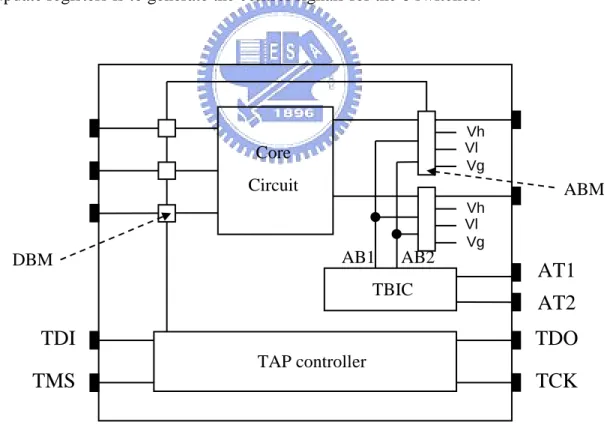
methodologies. In 1999, IEEE std.1149.4 was carried out for mixed-signal testing. We will introduce circuits and functions of main blocks for IEEE std.1149.4 below.
Figure 2.1 is the architecture of IEEE std.1149.4. There are 6 pins prepared for test I/Os. TCK is the test clock, TDI is the test data input, TDO is the test data output, TMS is the test
Chapter 2 Background
mode select, and AT1, AT2 are the analog test access ports. We can send test pattern into the scan chain and then obtain test results of each core blocks by connecting each boundary scan cell (DBM, ABM) together.
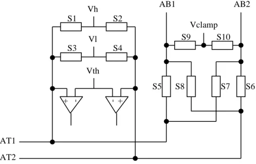
TAP controller, Test Access Port controller, is a very important block of the system. Its main objective is to facilitate board-level testing through boundary scan. TBIC, Test Bus Interface Circuit, is to connect internal test bus (AB1, AB2) and analog test access port (AT1,
AT2). Figure 2.2 shows the architecture of TBIC. In this figure, TBIC controls ten switches (S1~S10) depending on the control signals sent from TAP controller. Figure 2.3 is the main architecture of ABM. ABM means Analog Boundary Module, it consists of 6 switches (Sh, Sl, Sg, SB1, SB2, SD), control registers and update registers. The objective of control registers and update registers is to generate the control signals for the 6 switches.
Core Circuit Vh Vl Vg Vh Vl Vg TBIC TAP controller
TDI
TMS
TDO
TCK
AT1
AT2
DBM ABM AB1 AB2AT1 AT2 Vh Vl + - - + Vth AB1 AB2 Vclamp S1 S2 S3 S4 S5 S8 S7 S6 S9 S10
Figure 2.2 TBIC architecture
+ -+ -Vth Vh Sh Vl Sl Vg Sg SD SB1 SB2 Analog Pin AB1 AB2 TBIC AT1 AT2 Core Circuit
Figure 2.3 ABM architecture
The aim of the IEEE std.1149.4 research recently is to provide standardized approaches to interconnect test, parametric test and internal test [1], [2]. The first objective is to detect opens in the interconnections between integrated circuits. The second objective refers to the
Chapter 2 Background
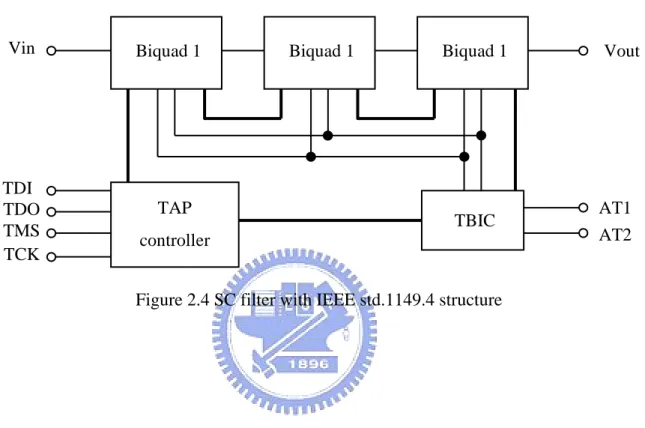
problem of measuring the values of discrete components. And the third objective refers to the ability to perform internal test of a component. In [2], they take SC filter as core circuit for example and simulate the whole circuit under normal mode and test mode. Figure 2.4 shows its structure.
Biquad 1 Biquad 1 Biquad 1
Vin Vout TDI TDO TMS TCK TAP controller TBIC AT1 AT2
Figure 2.4 SC filter with IEEE std.1149.4 structure
2.2 Research of SC Filter BISTs
In recent years, design-for-test and built-in-self-test technique for SC filters are popular fields of research. Many papers have been presented to apply different approaches to achieve on-chip test functions with minimum area and power overhead [3]-[6]. Here, we take [6] for example because of its novel ideas and complete circuit structures.
The objective in [6] is to discuss the possibility of reusing the existing hardware originally present in SC filters to implement test functions for a completely autonomous self-testable solution. The implementation of completely autonomous self-test implies the use
of on-chip Test Pattern Generators (TPGs) and Output Response Analyzers (ORAs). Figure 2.5(a) gives an example of analog filter made of a cascade of basic biquad clocks, and the TPG and ORA are added to the original circuit. The concept of this paper is shown in Figure 2.5(b). Some of the existing biquad blocks are reused in test mode to implement the TPG and ORA.
Biquad 1 Biquad 2 Biquad n
ORA TPG
Biquad 1
Biquad 1 Biquad 2Biquad 2 Biquad nBiquad n
ORA TPG
Figure 2.5(a) Classical BIST
Biquad 1 / TPG
Biquad 2 Biquad n
/ ORA
Figure 2.5(b) Reuse-based BIST
2.2.1 Multi-frequency TPG
The stimuli generator is a sine wave oscillator. As shown in Figure 2.6, this oscillator is based on two pure integrators connected in a ring configuration. A 360∘phase shift is ensured because the first integrator is inverting and the second integrator is non-inverting. Non-inverting integrator uses negative resistor, which is implemented by swapping two clock phases of a positive switched-capacitor [7].
Chapter 2 Background + -+ -Vout Va Csc Cosc Csc C C 1 φ 2 φ 1 φ 1 φ 1 φ 1 φ 1 φ 2 φ 2 φ 2 φ 2 φ 2 φ Figure 2.6 TPG
From Figure 2.6, oscillation frequency of TPG is given by
C
C
f
f
clk sc oscπ
2
⋅
=
. (2-1)The negative SC resistor in the local feedback loop of the first integrator results in a positive feedback. It ensures circuit instability and a faster growth in the oscillation amplitude. The bias voltage Va is used to adjust the amplitude of the oscillation.
2.2.2
Multi-frequency ORA
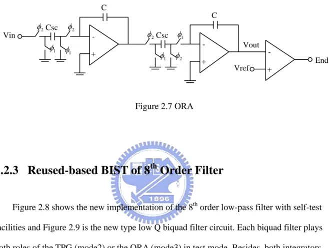
As shown in Figure 2.7, the ORA is also based on cascade of two integrators and an additional comparator. A digital signature is obtained by computing the time for the output of the second integrator to reach Vref. There is a counter for computing digital signatures, and
this counter must be enabled from the integration start up to the time when the comparator output goes high [8], [9].
+ -Csc C 1 φ 1 φ 2 φ φ2 Vin + -Csc C 1 φ 1 φ 2 φ 2 φ + -Vref End Vout Figure 2.7 ORA
2.2.3 Reused-based BIST of 8
thOrder Filter
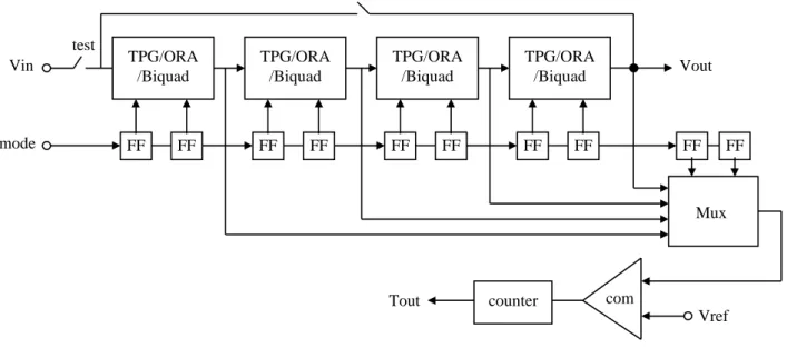
Figure 2.8 shows the new implementation of the 8th order low-pass filter with self-test facilities and Figure 2.9 is the new type low Q biquad filter circuit. Each biquad filter plays both roles of the TPG (mode2) or the ORA (mode3) in test mode. Besides, both integrators can be reset by shortening their integration capacitors (mode4). The operation mode of a given biquad filter is determined by two bits in two flips-flops. Only one comparator is added to the whole circuit and connected to each biquad filter output through a multiplexer.
Chapter 2 Background TPG/ORA /Biquad TPG/ORA /Biquad TPG/ORA /Biquad TPG/ORA /Biquad test Vin mode FF FF FF FF FF FF FF FF FF FF Mux Vref counter com Tout Vout
Figure 2.8 Self-testable 8th order low-pass filter topology
+ -C1 Ca Vin + -C2 Cb C4 mode4 C3 mode3 mode2 mode4 Vout
The test procedure includes 4 phases, each phase being dedicated to the test of one of the biquad filters. For example, if the second biquad filter is tested, then the first biquad filter acts as the TPG and the third one as the ORA. In the next phase, test functions are moved to the next blocks so the third biquad filter is tested in this phase.
The self-test method presented in [6] is innovative, but there are still some problems exist when we realize it for circuit implementation. First, each biquad filter is able to perform its normal function, work as sine wave oscillator, or as a signature analyzer. This
characteristic can effectively decrease area overhead. But, performance of the core circuits is also affected because we change the structure of biquad filters. Second, design of a sine wave oscillator is complex and we can not generate the sine wave actually. This will affect the precision of test results.
2.3 Concept and Formula Derivation
In this thesis, we will use different concepts and methods from [6] to avoid its main drawbacks. First, we use triangular-wave as test waveform to replace sine wave. Therefore, we can implement a high resolution test waveform. Second, we use a pair of comparators called dual-comparator to replace single comparator. According to the dual-comparator analysis, we can divide a triangular-wave into 3 portions. Therefore, we can compute the probabilities of each portion. Moreover, we can also obtain the probabilities when the triangular-wave has different values of offset and amplitude. Finally, we can obtain the information about gain error and offset error of the core circuits by comparing the probability
Chapter 2 Background
of the self-test results to the derived ones.
Figure 2.10 shows the concepts of our method. In this figure, Va is the amplitude of the triangular-wave, Vx is offset of the triangular-waves, and Vr+, Vr- are the reference values of the dual-comparator. Vx Vr-Vr+ P3 P2 P1 Va
Figure 2.10 Concept of method
P1 is the probability of that the triangular-waves are lower than Vr-. P2 is the probability of that the triangular-waves are between Vr+ and Vr-. And P3 is the probability of that the triangular-waves are higher than Vr+. According to the formula derivation we can obtain the equations of P1, P2 and P3 as . 0 . 2 ) ( 2 1 . 2 ) ( 2 1 : 1 CASE 3 2 1 = − + = − − = < + − − + P V V V P V V V P V V V A R X A R X R A X . (2-2)
. 2 ) ( 2 1 . 2 ) ( . 2 ) ( 2 1 , : 2 CASE 3 2 1 A X R A R R A R X R A X R A X V V V P V V V P V V V P V V V V V V − − = − = − − = < − < + + − + − − + . (2-3) . 2 ) ( 2 1 . 2 ) ( 2 1 . 0 : 3 CASE 3 2 1 A X R A X R R A X V V V P V V V P P V V V − − = − + = = > − + + − . (2-4)
Chapter 3 Switched-capacitor Low-pass Filter
Chapter 3
Switched-capacitor Low-pass Filter
Switched-capacitor (SC) filters have become extremely popular due to their accurate frequency response, linearity, and dynamic range. Since coefficients of SC filters are determined by capacitance ratios which can be set precisely in ICs (on the order of 0.1%), accuracy of SC filters are much better than RC filters (as much as 20%).
A SC filter is realized with some basic building blocks such as opamps, capacitors, switches, and nonoverlapping clocks. We will detail the objectives, circuit structures and design considerations of these building blocks in this chapter.
3.1 Fully Differential, High Bandwidth Opamp
nonidealities affect the accuracy of SC circuits such as DC gain, unity-gain frequency, phase margin and slew rate.
The DC gain of opamps in a CMOS technology is typically on the order of 60dB. Low DC gain affects the accuracy of the discrete-time transfer function.
The unity-gain frequency (Ft) and phase margin (PM) of an opamp gives an indication of the small signal settling behavior of an opamp. A general rule is that Ft should be at least 5 times larger in frequency than the clock frequency assuming little slew rate behavior occurs and PM is greater than 60∘. Modern SC filters are realized using high-frequency single-stage opamps such as folded-cascode opamps or telescopic opamps. These opamps have very large output impedances (on the order of 100K Ohm) since the loads are purely capacitive, instead of resistive.
The finite slew rate (SR) of opamps can limit the clock frequency in SC filters as these circuits rely on charge being quickly transferred from one capacitor to another. Thus, at the instance of charge transfer, it is uncommon for opamps to exceed SR limit.
3.1.1
Fully-Differential Structure
In most analog applications, it is desirable to keep the signals in differential mode. Fully-differential signals imply that the difference between two lines represents the signal component. Thus, any noise appears as a common-mode signal on those two lines does not affect the signal. Fully differential circuits should also be balanced, implying that the
differential signals operate symmetrically around a DC common-mode voltage which is called analog ground. Fully differential circuits have another advantage that if each single-ended
Chapter 3 Switched-capacitor Low-pass Filter
will have only odd-order distortion terms. These terms are often much smaller. Consider the block diagram shown in Figure 3.1, two nonlinear elements are identical and then each of the outputs can be found as a Taylor series expansion given by
...
3 3 2 2 1⋅
+
⋅
+
⋅
+
=
i i i ok
V
k
V
k
V
V
, (3-1)where ki are constant terms. In this case, the differential output signal, Vdiff, consists of only the odd-order terms,
...
2
2
2
1⋅
+
3⋅
3+
5⋅
5+
=
i i i diffk
V
k
V
k
V
V
. (3-2)With these two important advantages, most modern switched-capacitor circuits are realized using fully differential structures.
Nonlinear element Nonlinear element Vi -Vi Vo1 Vo2
+
Vdiff Figure 3.1In this thesis, we introduce folded-cascode opamp as our opamp structure. We expect Ft of the opamp to be 5 times greater than clock frequency (140 MHz), and under this condition, we still have great DC gain about 60dB to reduce the gain error.
In the next parts, design considerations of the opamp and bias circuit for the opamp are described in detail. Finally, we compare pre-layout simulation and post-layout simulation results of the opamp.
3.1.2 Design considerations
Table 3.1 shows characteristics of three types of opamps. There are some critical points in choosing which one is suitable for our design. First, if we need high bandwidth, two-stage opamps is not a good choice. Second, we define VDD as 1.8V for CMOS 0.18um technology, so output swing is a critical issue of our design. We can find that telescopic opamps are not applicable with its low output swing. So, in this thesis, we take folded-cascode opamp as the structure to implement opamp.
Output Power
Gain Swing Speed Dissipation Noise
Telescopic medium Low high Low low
Folded-Cascode medium medium high High medium
Two-Stage High High low medium low
Table 3.1 Comparison of three types of opamps
Figure 3.2 is the structure of a typical fully-differential folded-cascode opamp. It has many advantages such as high bandwidth, high DC gain concurrently, and high dynamic range. However, its main drawback is the power dissipation. Compared to telescopic structure, folded-cascode has two current branches (differential input pair and cascode current mirror
Chapter 3 Switched-capacitor Low-pass Filter
Figure 3.2 Typical fully-differential folded-cascode opamp
Typically, when using fully-differential opamps in a feedback application, the applied feedback determines the differential signal voltages, but does not affect the common-mode voltages. Therefore, it is necessary to add an additional circuit to determine the output
common-mode voltage and to control it to be equal to the analog ground. This circuit is called common-mode feedback (CMFB) circuitry. CMFB has many drawbacks we can not overcome
and these drawbacks will affect opamp performs. First, it is often the most difficult part of the opamp design. Second, there are two typical approaches to implement CMFB circuits, a continuous-time approach and a switched-capacitor approach. The former approach usually limits the signal range. And, if nonlinear, it may introduce common-mode signals. The latter one will increase additional capacitance loadings to the main circuit and then reduce
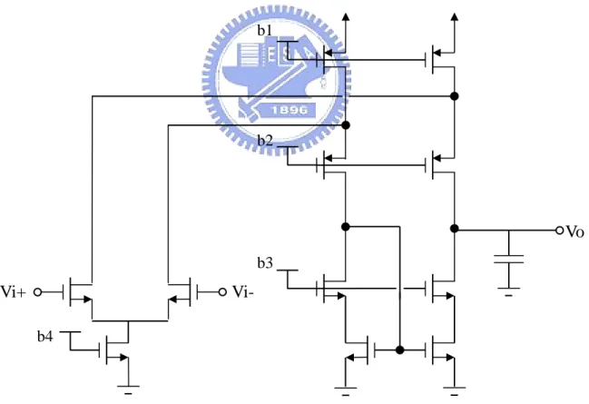
bandwidth of the opamp. Switched-capacitor CMFB may also introduce clock-feedthrough Vi-Vi+ Vo+ CMFB Vo- b1 b2 b3 b4
glitches.
To avoid the disadvantages of CMFB but achieve fully-differential structure, we use the approach in [10]. Figure 3.3 is a typical single-ended folded-cascode opamp. We use cascode current mirror to obtain wide-swing output range. Because a single-ended folded-cascode opamp has excellent Common-mode Rejection Ratio (CMRR), it has robust common-mode output voltage and tiny effects from noises and distortions. Due to these characteristics, we can implement a fully differential folded-cascode opamp without CMRR by two single-ended ones with inverse differential inputs. Figure 3.4 shows this concept. This structure can
improve the bandwidth. Unfortunately, it has larger power dissipation than the typical one.
Figure 3.3 Typical single-ended folded-cascode opamp
Vi-Vi+ Vo b1 b2 b3 b4
Chapter 3 Switched-capacitor Low-pass Filter
+
-+
Vi+ Vi- Vo-Vo+Figure 3.4 Concept of fully differential opamp presented in [10]
3.1.3 Fully differential, High Bandwidth Opamp
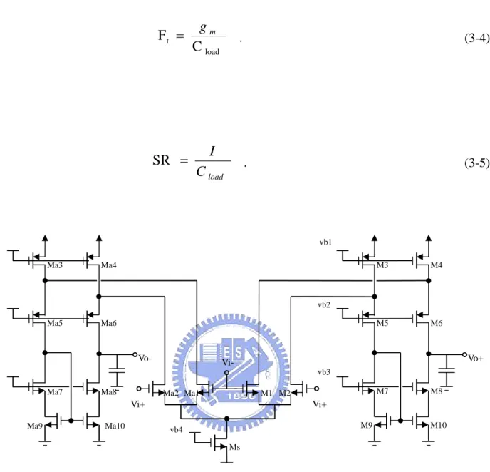
With recent technologies, High gains become more difficult to achieve because of short-channel effect. We let channel length as 0.36um here for the consideration of DC gain and to reduce the process variation concurrently. Figure 3.5 is the circuit structure of fully differential, high bandwidth opamp we use in this thesis. We set output loadings 2pF, current goes through Ms is 4.2mA and goes through M3,4, Ma3,4 is 1.9mA. Under these conditions, we obtain transconductance of differential input pair (M1,2 , Ma1,2) to be 15.8m (1/Ohm) and output impedance to be 51K (Ohm). Then, according to (3-3~5) we can compute
specifications of the opamp as: DC gain=58.2 dB, Ft=790 MHz and Maximum SR=950 us/sec. out m
r
g
⋅
=
gain
DC
. (3-3)load t
C
F
=
g
m . (3-4) loadC
I
=
SR
. (3-5)Figure 3.5 fully differential, high bandwidth opamp
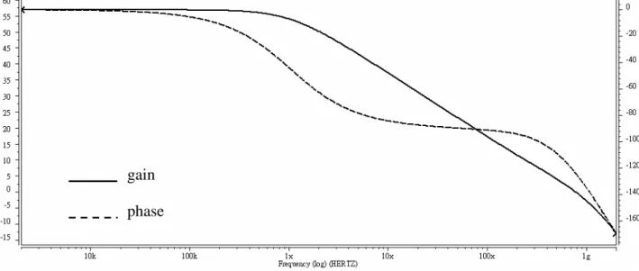
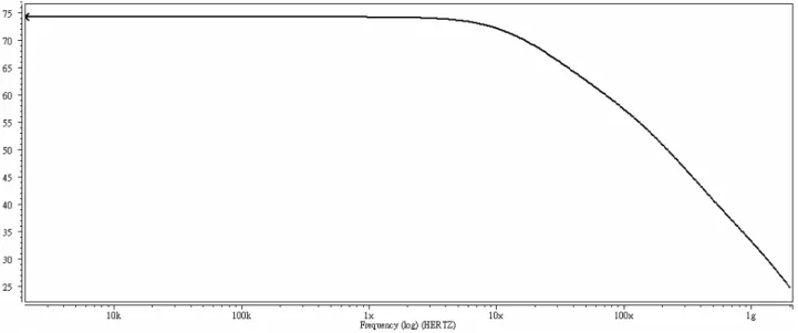
Figure 3.6 is the frequency response simulation results of the opamp. It shows that the dominate pole falls into 1 MHz and the first nondominate pole falls into 990 MHz. At low frequency, DC gain is 57.1 dB (DC gain). The unity-gain frequency is 783 MHz and the phase margin is 57∘.
Figure 3.7 is the CMRR simulation results. The CMRR is 74.3 dB at low frequency.
Vo+ vb4 vb2 vb3 Vo- Vi-Vi+ Vi+ Ms M1 M2 Ma2 Ma1 M3 M4 M5 M6 M7 M8 M9 M10 Ma3 Ma4 Ma5 Ma6 Ma7 Ma8 Ma9 Ma10 vb1
Chapter 3 Switched-capacitor Low-pass Filter
Figure3.8 is the simulation results of SR. We connect the opamp positive output and negative input together to become a unity-gain buffer. Use ideal square waves as input signal to obtain the SR simulation results. It shows that at rising edge SR is 552 us/sec (SR+) and at falling edge SR is 435 us/sec (SR-).
According to these data, we find that the simulation results are very close to the computing values according to the formulas.
Figure 3.6 Frequency response simulation gain
Figure 3.7 CMRR simulation
Figure 3.8 SR simulation
Table 3.2 shows the specifications summary of the opamp. It also shows the post-layout simulation results to compare with the pre-layout simulation results. For layout consideration, we use Source-Drain Merge method to reduce parasitic capacitor at the output of the opamp. Although using common-centroid method can reduce the input offset, it also increase parasitic
in out
Chapter 3 Switched-capacitor Low-pass Filter
capacitor at input pair and decrease the Ft. So in this thesis we adopt traditional method for the opamp layout in order to hold the high bandwidth. Figure 3.9 is the layout of the fully differential, high bandwidth opamp, the area is 275 * 75 um2.
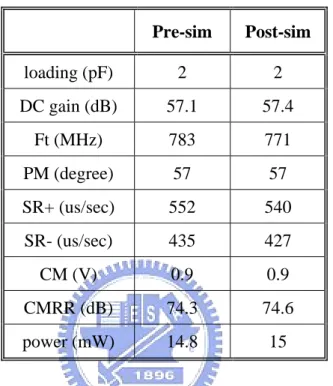
Pre-sim Post-sim loading (pF) 2 2 DC gain (dB) 57.1 57.4 Ft (MHz) 783 771 PM (degree) 57 57 SR+ (us/sec) 552 540 SR- (us/sec) 435 427 CM (V) 0.9 0.9 CMRR (dB) 74.3 74.6 power (mW) 14.8 15
Table 3.2 Specifications summary of the fully differential, high bandwidth opamp
3.1.4 Wide-swing Constant-transconductance Bias Circuit
Besides the main circuit of the opamp described in the above section, bias circuit is also an important part. Its main function is to apply steady, noise-insensitive voltage for biasing points of the opamp. In this thesis, we introduce a wide-swing, constant-transconductance bias circuit to implement the biasing circuit. It consists of the start-up circuit to prevent the circuit working at unexpected steady state.
Perhaps the most important parameters in opamps are the transconductance of transistors. Figure 3.10 is a bias circuit that gives very stable transconductances. With this method, to a first-order effect, the transconductances are independent of power-supply as well as process and temperature variations.
Figure 3.10 Bias circuit with stable transistor transconductances M1 M2 M3 M4 M5 M6
Chapter 3 Switched-capacitor Low-pass Filter
Assuming the sizes of M5 and M6 are equal and the circuit has the same current (ID) due to the current-mirror pair. As a result,
R
I
V
V
gs1=
gs2+
D⋅
. (3-6) Recalling that t gs effV
V
V
=
−
. (3-7)We can subtract the threshold voltage from both sides in (3-6) and rewrite (3-6) as
R
I
L
W
C
I
L
W
C
I
D ox n D ox n D=
+
⋅
2 1(
)
2
)
(
2
µ
µ
. (3-8)And recalling that
1 1 1
2
n ox(
)
D mI
L
W
C
g
=
µ
⋅
. (3-9)We obtain the important relationship
R
L
W
L
W
g
m]
)
/
(
)
/
(
1
[
2
2 1 1−
=
. (3-10)Thus, the transconductance of M1 is determined by geometric ratios only, independent of power-supply, process parameters, temperature or other parameters with large variability. For the special case of (W/L)2=(W/L)1, we can find
R
g
m1=
1
. (3-11)As new technologies with shorter channel lengths are used, designers are often forced to use cascode current mirrors to achieve high gain. Unfortunately, the use of conventional cascode current mirror limits the signal swings, this drawback reduces the circuit practicality. One novel structure of cascode current mirrors that do not limit the signal swings is shown in Figure 3.11, which is called the wide-swing cascode current mirror.
Figure 3.11 Wide-swing cascode current mirror
The basic idea of this current mirror is to bias the drain-source voltages of transistors M2 and M3 to be close to the minimum possible without going into the triode region. Note that the transistor pair M3, M4 acts like a single diode-connected transistor in creating the
gate-source voltage for M3. The reason for including M4 is to lower the drain-source voltage of M3 so that it is matched to the drain-source voltage of M2. This matching makes Iout more accurately match Iin.
M5 M4
M3
M1
M2
Chapter 3 Switched-capacitor Low-pass Filter
To determine the bias voltages for this circuit, we have
L
W
C
I
V
V
V
ox n D eff eff effµ
2 3 22
=
=
=
. (3-12)Furthermore, we let size of M1~M4 be the same and 4 times greater than that of M5, then we have eff eff eff eff eff
V
V
V
V
V
⋅
=
=
=
2
5 4 1 . (3-13) Thus, eff gs gs ds dsV
V
V
V
V
2=
3=
5−
1=
. (3-14)So, M2 and M3 are at the edge of the triode region. Thus, the minimum allowable output voltage is eff eff eff out
V
V
V
V
>
1+
2=
2
⋅
. (3-15)According to the two concepts we have introduced, we incorporate wide-swing current mirrors into the constant-transconductance bias circuit. This circuit minimizes most of the second-order imperfections caused by the finite-output impedance of the transistors. Without greatly restricting signal swings. The complete circuit is shown in Figure 3.12.
Figure 3.12 Wide-swing constant-transconductance bias circuit
This bias circuit does have the problem that it is possible for the current to be zero in all transistors, and the circuit will remain in the stable state. It is necessary to include start-up circuitry. An example of a start-up circuit consisting M15 ~ M18 is shown in Figure 3.12. If
all currents in the bias loop are zero, M17 will be off. Since M18 operates as a
high-impedance load that is always on, the gate voltages of M15, M16 will be pulled high and these transistors will inject currents into the bias loop. Once the Bias loop starts up, M17 will turn on and then pull the gate voltages of M15, M16 low. Finally, start-up circuitry will be turned off and no longer affects the bias loop.
The simulation result of the whole bias circuit is shown in Figure 3.13. In this figure, we set the initial currents of all transistors are zero. Thus, the initial values of b1, b2 are 1.8 V
R 0.17mA
b1
b2
b3 b4
Bias loop Cascode loop Start-up
M2 M3 M1 M4 M9 M6 M8 M7 M5 M10 M11 M14 M13 M12 M15 M18 M17 M16
Chapter 3 Switched-capacitor Low-pass Filter
and b3, b4 are 0 V. Due to the start-up circuitry, the four bias points will work at normal stable state after 5 nsec.
Figure 3.13 Simulation results of the Wide-swing constant-transconductance bias circuit
3.2 SC Low-pass Filter
3.2.1 Resistor Equivalence of a Switched capacitor
Consider the switched-capacitor circuit shown in Figure 3.14. Assuming φ and1 φ are 2 two nonoverlapping clocks. C is charged to V1 and then V2 during each clock period.
)
(
V
1V
2C
Q
=
−
∆
. (3-16)Then, we can also find the equivalent average current over one clock period is given by
T
V
V
C
I
avg=
(
1−
2)
, (3-17)where T is the clock period. Finally, we see the equivalent resistor of the switched capacitor in Figure 3.14 over one clock period is given by
s eq eq
f
C
C
T
I
V
V
R
⋅
=
=
−
=
1 21
, (3-18)where fs is the sampling frequency.
Figure 3.14 SC resistor
In Figure 3.14, we ignore the effect of the parasitic capacitors. Here, Cp represents the parasitic capacitor of the top plate of C as well as the nonlinear capacitors associated with the two switches. It is in parallel with C and therefore cause gain error of the circuit transfer function. To overcome this drawback, parasitic-insensitive structures have been developed to
V1 V2
C
1
φ φ2
Chapter 3 Switched-capacitor Low-pass Filter
realize high accuracy. Figure 3.15(a) is a parasitic-insensitive resistor equivalence of switched capacitor in positive type and Figure 3.15(b) is the negative one.
Figure 3.15 (a) Positive parasitic-insensitive SC resistor
Figure 3.15 (b) Negative parasitic-insensitive SC resistor
3.2.2 Signal-flow-graph Analysis of Low-pass Biquad Filter
The transfer function of typical continuous-time biquad filters are given by
2 0 0 2 0
)
(
)
(
)
(
)
(
ω
ω
⋅
+
+
−
=
≡
s
Q
s
k
s
V
s
V
s
H
i o , (3-19) V1 V2 1 φ C 1 φ 2 φ 2 φ V1 V2 1 φ C 1 φ 2 φ 2 φwhere ω0 represents the corner frequency and Q is called Q factor. Signal-flow-graph is
shown in Figure 3.16.
Figure 3.16 Signal-flow-graph of continuous-time biquad filter
We can transfer the signal-flow-graph from S-domain (Figure 3.16) into Z-domain (Figure 3.17) for discrete-time biquad filters, and according to Figure 3.17, the transfer function of the discrete-time biquad filters, H(z), are found to be
1
)
2
(
)
1
(
)
(
)
(
)
(
4 3 2 2 4 3 1+
⋅
−
−
+
⋅
+
⋅
−
=
≡
z
K
K
K
z
K
z
K
K
z
V
z
V
z
H
i o (3-20)Figure 3.17 Signal-flow-graph of discrete-time biquad filter
+
Vi(s)
s 1 − 0 0 ω k s 1 −+
0 ω − Q 0 ω 0 ωVo(s)
+
Vi(z) 1 1 1 − − z 1 K −+
1 3 − ⋅ z K 4 K − 2 K − Vo(s) 1 1 1 − − zChapter 3 Switched-capacitor Low-pass Filter
Finally, comparing Figure 3.16 and Figure 3.17 we can find the approximations for feedback capacitor ratios are given by
T
K
K
2≈
3≈
ω
0 . (3-21)Q
T
K
0 4ω
≈
. (3-22) 2 1(
DC
gain
)
K
K
≈
⋅
. (3-23)A switched-capacitor low-pass biquad filter based on Z-domain signal-flow-graph is shown in Figure 3.18. Note that this SC biquad filter has redundant switches, as switch sharing has not yet been applied.
1 φ + -+ -Vi(z) Vo(z) K1C1 C1 C2 1 φ 2 φ φ2 1 φ K2C1 1 φ 2 φ φ2 φ1 K4C1 φ1 2 φ φ2 1 φ K3C1 φ1 2 φ 2 φ
Figure 3.18 Switched-capacitor Low-pass biquad filter
In this thesis, we set ω0T =0.45 and sampling frequency to be 140 MHz due to limitation of the opamp bandwidth, so corner frequency of the biquad filter will be 10 MHz. We also set Q factor and DC gain of the biquad filter to be unity. Then, we can see all capacitor values of the biquad filters shown in Table 3.5.
C1 C2 K1C1 K2C2 K3C2 K4C2
1.5 pF 1.5 pF 0.675 pF 0.675 pF 0.675 pF 0.675 pF
Table 3.3 Capacitor values of the biquad filter
3.2.3 Switches
The requirements for switches used in SC filters must have a very high off resistance, a relatively low in resistance, and no offset voltage when it turns on. In today’s CMOS
technology, using of MOSFET transistors as switches satisfies these requirements.
MOS switches consist of NMOS, PMOS and CMOS switches, like Figure 3.19 shows. NMOS switches are applicable for low voltage range and PMOS switches are applicable for high. However, CMOS switches combine the advantages of both ones. It can work for full range. Figure 3.20 shows method to simulate the turn-on resistance of MOS switches [11]. We use AC current as input signal and then obtain drain-source voltage of the switch as output signal. Inductors in this figure are used to make sure that AC signals only pass through MOS switches. Therefore, turn-on resistance of the switch is given by
Chapter 3 Switched-capacitor Low-pass Filter in out onP onN on
I
V
R
R
R
=
//
=
. (3-24)Figure 3.19 3 types of MOS switches
gnd vdd
gnd vdd
NMOS switch PMOS switch CMOS switch
φ φ
φ
φ Vdc Vdc gnd vdd L L Vout IinFigure 3.21 is the CMOS switches turn-on resistance simulation results. Different figures represent different ratios between NMOS sizes and PMOS sizes. We simulate overall four kinds of ratios that NMOS sizes over PMOS sizes are 1/2, 1/3, 1/4 and 1/5. In these simulation results we find that when NMOS size over PMOS size is 1/4, the turn-on resistance of CMOS switches is mostly like constant. Besides, we also see that larger sizes bring lower turn-on resistances. However, we have to consider non-ideal effects of MOS switches such as charge-injection and clock-feedthrough, which introduce errors proportional to the switch sizes when we design MOS switches. Therefore, determination of MOS switch sizes is a trade-off between turn-on resistance and non-ideal error.
Vdc 0.5 0.6 0.7 0.8 0.9 1.0 1.1 1.2 1.3 Ron 0 100 200 300 400 6u - 24u 8u - 32u 10u - 40u Vdc 0.5 0.6 0.7 0.8 0.9 1.0 1.1 1.2 1.3 Ro n 0 100 200 300 400 6u - 30u 8u - 40u 10u - 50u Vdc 0.5 0.6 0.7 0.8 0.9 1.0 1.1 1.2 1.3 Ro n 0 100 200 300 400 6u - 12u 8u - 16u 10u - 20u Vdc 0.5 0.6 0.7 0.8 0.9 1.0 1.1 1.2 1.3 Ro n 0 100 200 300 400 6u - 18u 8u - 24u 10u - 30u
Chapter 3 Switched-capacitor Low-pass Filter
Non-ideal effects of MOS switches are the major limitation on resolution of SC circuits. They cause error due to unwanted charges being injected into the circuit when switches turn off. Non-ideal effects include two types called charge injection and clock feedthrough. We have more detail analysis of these two effects in Figure 3.22 and next description.
Figure 3.22 Non-ideal effects of MOS switches
(1) Charge Injection: Charge injection occurs by channel charge when MOS switches turn off. From Figure 3.22 we can see the channel charge flow out from the channel region of the transistor to the drain and source junctions. The channel charge of a transistor had zero drain-source voltage is given by
)
(
gs t ox eff ox chWLC
V
WLC
V
V
Q
=
=
−
. (3-25)And we derive voltage error due to charge injection is given by
G
φ
Cov CovVi
Vo
S D
Cl
Qch hφ
lφ
l t gs ox ov l ch
C
V
V
WLC
C
C
Q
V
2
)
(
1
2
1
≈
−
−
+
⋅
−
=
∆
. (3-26)(2) Clock Feedthrough: From Figure 3.22, overlap capacitors between gate and junctions will inject additional charge into circuit when switches turn off, and this effect is called clock feedthrough. Voltage error due to clock feedthrough is given by
ov l ov l h
C
C
C
V
+
⋅
−
−
=
∆
(
φ
φ
)
, (3-27) where φh is VDD and φl is Gnd.Due to (3-26) and (3-27) we find that error caused by clock feedthrough is small and signal-independent, which can be eliminated by fully-differential structure. On the other hand, error caused by charge injection is much larger. We also can divide charge injection into two parts, signal-dependent and signal-independent. Switches connected to analog ground and virtual ground will cause signal-independent error because its turn-on voltage is constant. Just like clock feedthrough, we can eliminate this kind of errors duo to fully-differential structure. Besides these, switches connected to the signal will cause signal-dependent error which is changed with signal. Signal-dependent error is important because it truly affects resolution of the circuit. Therefore, How to reduce this kind of errors is the critical issue when we design switches of SC filter. In this thesis, we use three kinds of approaches to reduce charge injection and have description about these approaches as below.
(1) The first approach to lower charge injection effect is incorporating both NMOS and PMOS devices that have same charge amount but opposite direction as a CMOS switch. This approach can make channel charges of two different transistors cancel
Chapter 3 Switched-capacitor Low-pass Filter
(2) Using dummy switches. As Figure 3.23 shown, a dummy switch (M2) driven by inverse clock is added to the circuit. Therefore, the charge injected by the main switch (M1) can be removed to M2 after M1 turns off and M2 turns on. Note that both source and drain of M2 are connected to the output node and M2 has half size of M1 in order to make∆q1= ∆q2.
(3) The third approach is called bottom-plate sampling. Here, we take an SC integrator as example. As Figure 3.24 shows, we add a pair of clocks (φ1a,φ2a) that slightly
advance than original clocks (φ ,1 φ ). When M1 turns off, the injected charge2 ∆q1
will not cause any change in the charge stored in Cl since M2 has already turned off and the right side of C1 is connected to an effective open circuit. Therefore, by this approach, the circuit is affected only by M2 and M4 which are connected to virtual ground or analog ground. Charges injected by these transistors are
signal-independent and be cancelled by fully-differential structure.
Figure 3.23 Addition the dummy switch to reduce charge injection
φ Vi φ Cl Vo M1 M2 1 q ∆ ∆q2
Figure 3.24 SC integrator with bottom-plate sampling
Due to concepts of turn-on resistance and charge injection cancellation we have described, now we can determine the sizes of MOS switches.
At beginning, we take a biquad filter as two first-order system with a single delay around the loop due to the negative SC resistor. And the output error of an ideal first-order system is given by
τs
t
e
t
e
V
(
)
=
− , (3-28)where τ is RC time constant of the first-order system and t is settling time of the s
first-order system. Assuming the circuit has N bits resolution, then (3-28) can be rewritten as
1
2
1
+ −≤
N tse
τ . (3-29)We set capacitance loading as 2 pF, settling time as half of clock period and resolution as 8 bits, then we can obtain the term of turn-on resistance limitation given by
+ -C1 C2 Vo 1 φ φ1a 2 φ φ2a 1 q ∆ ∆q2 M1 M2 M3 M4 Vi
Chapter 3 Switched-capacitor Low-pass Filter
K
p
n
C
N
t
R
l s on0
.
28
2
2
ln
9
57
.
3
2
ln
)
1
(
+
⋅
⋅
=
⋅
⋅
≈
≤
. (3-30)Due to (3-30) we can determine the size of NMOS switches. As for CMOS switches, we still have to consider the size ratio between NMOS and PMOS.
How to determine the ratio? First of all, we recall that the equation of transistor current versus voltage at triode region is given by
]
2
1
)
)[(
(
gs t ds ds2 ox dV
V
V
V
L
W
C
I
=
µ
−
⋅
−
. (3-31)And then turn-on resistance of MOS switches is given by
eff ox ds d on
V
L
W
C
V
I
R
⋅
=
∂
∂
=
−)
(
1
)
(
1µ
. (3-32)Due to (3-25), (3-32) and MOS parameters such as mobility and threshold voltage, the optimize size ratio between NMOS and PMOS of a CMOS switch can be derived as below.
First, we set Ron of NMOS to be equal to that of PMOS, then we obtain
) ( ) ( ) ( ) (
)
/
(
)
/
(
1
n ov n n ox n p ov p p ox p p on n onV
L
W
C
V
L
W
C
R
R
µ
µ
=
=
. (3-33) (3-33) can be rewritten as23
.
4
)
/
(
)
/
(
≅
n n p pL
W
L
W
. (3-34)(3-34) shows the computing result is fit in with the simulation result in Figure (3-21).
Second, to reduce charge injection effect, we set channel charge of NMOS and PMOS are the same. Then we get
) ( ) ( ch(p) ch(n)
1
p ov ox p p n ov ox n nV
C
L
W
V
C
L
W
V
V
⋅
⋅
⋅
⋅
=
=
. (3-35) (3-35) can be rewritten as73
.
0
≅
⋅
⋅
p p n nL
W
L
W
. (3-36)Due to (3-34) and (3-36), ratios of channel width and length between NMOS and PMOS are given by
0.42
,
1.77
=
=
p n p nW
W
L
L
. (3-37)Finally, according to (3-30) and (3-37), we can determine the sizes of CMOS switches.
3.2.4 Nonoverlapping Clocks
Clocks determine when charge transfers occur and they must be nonoverlapping in order to guarantee charge is not lost. One simple approach for generating nonoverlapping clocks is shown in Figure 3.25. Here, delay blocks are used to ensure clocks are nonoverlapping with each other.
Chapter 3 Switched-capacitor Low-pass Filter
Figure 3.26 is the output buffer of nonoverlapping clocks to generate the final clock and its inverse clock applied for the SC filter. The transmission gates are used to match the clock and its inverse clock. Figure 3.27 shows the complete circuit of the clock driver. Because of bottom-plate sampling, we need two pairs of nonoverlapping clocks.
Figure 3.25 Circuit implementation of nonoverlapping clocks
Figure 3.26 Output buffer of nonoverlapping clocks clk delay delay 1 φ 2 φ inv1 inv2 tr1 inv3 in φ φ
Figure 3.27 Clock driver
3.2.5 Simulation Results of the SC Low-pass Filter
Figure 3.28 shows the low-pass biquad filter circuit structure. Some redundant switches are removed due to the concept of switch sharing. Switches that connected to analog ground or virtual ground will be implemented with NMOS switches because they are always working at 0.9V when turn on. Other switches connected to the signal will be implemented with CMOS switches for working at wide range. Capacitor values have been already introduced in Table 3.5. 1a φ φ1 2 φ clk 2a φ a 1
φ
φ1 2 φ a 2 φChapter 3 Switched-capacitor Low-pass Filter b 1 φ 1 φ + -Vi+ Vo+ 0.675p 1.5p 1.5p a 1 φ 2 φ φ2a 2 φ a 2 φ 2 φ a 1 φ 0.675p 0.675p 0.675p + -2 φ 0.675p a 2 φ a 1 φ 2 φ 0.675p a 2 φ + -+ -1.5p 0.675p a 2 φ 0.675p 1.5p Vi- Vo-1 φ b 1 φ 1 φ b 2 φ 1 φ b 2 φ 1 φ b 1 φ 1 φ b 1 φ a 1 φ b 1 φ 1 φ + -Vi+ Vo+ 0.675p 1.5p 1.5p a 1 φ 2 φ φ2a 2 φ a 2 φ 2 φ a 1 φ 0.675p 0.675p 0.675p + -2 φ 0.675p a 2 φ a 1 φ 2 φ 0.675p a 2 φ + -+ -1.5p 0.675p a 2 φ 0.675p 1.5p Vi- Vo-1 φ b 1 φ 1 φ b 2 φ 1 φ b 2 φ 1 φ b 1 φ 1 φ b 1 φ a 1 φ
Figure 3.28 Fully-differential low-pass biquad
Finally, we implement a fully differential, high bandwidth, 4th-order SC low-pass filter due to two cascading biquad. Figure 3.29 is the frequency response simulation results. In this figure, we see that pre-layout simulation results are very close to post-layout simulation results, and maximum error between ideal filter and the SC filter is 0.8dB at 8 MHz.
Figure 3.29 Frequency response simulation results
Figure 3.30 shows the harmonic distortion simulation results of the SC filter. The input single tone is at about 1/3 of the corner frequency in order to capture the worst case for the dominant third harmonic [12]. In this figure, we see the maximum harmonic distortion is -43 dB at corner frequency. Finally, we list specifications of the fully-differential, high bandwidth, 4th-order SC low-pass filter in Table 3.4.
* Ideal
X Pre-simulation O Post-simulation
Chapter 3 Switched-capacitor Low-pass Filter
Figure 3.30 Harmonic distortion simulation result
Sampling Frequency 140 MHz Corner Frequency 10 MHz DC Gain 1 T 0 ω 0.45 Q Factor 1 CM Voltage 0.9 V Signal Range 0.65 V ~ 1.15 V Max. Harmonic Distortion -43 dB
Table 3.4 Specifications summary of the fully differential, high bandwidth, 4th-order SC low-pass filter
Chapter 4
Built-in-self-test Circuit
How to achieve on-chip test function of SC filters with limited area and power overhead is the critical issue for mixed-signal testing designers. It is also the top target of this thesis. Test concept and method we adopted have already been introduced in Chapter 2, section 3. In this chapter, we will describe how to transfer the ideas into the hardware circuits. The circuit implementation will include a triangular-wave oscillator to take as test-waveform-generator (TWG), a differential-to-single-ended circuit with a dual-comparator to take as output response analyzer (ORA). The triangular-wave oscillates at 29.2 KHz. We determine a very
low frequency here in order to increase accuracy of the triangular-wave itself and linearity of the core circuit (SC filter) output response.
In the last section of this chapter, we will introduce layout considerations of the SC filter and the BIST circuit. Total area of the chip is 1.65(mm)*1.3(mm) and total power is 72 mW.
Chapter 4 Built-in-self-test Circuit
4.1 Test-waveform-generator
Figure 4.1 shows a pair of differential triangular-waves. In this figure, we see some critical specifications to adjust the performance of differential triangular-waves are:
(1) Amplitude (Va): voltage amplitude error of the triangular-wave will cause error of signal swing. Here, we use a pair of dual-comparator to take as the amplitude judgment device. Oscillation frequency of the triangular-wave is very low to reduce the comparator offset voltage.
(2) Phase shift (∆ ): Phase shift between each of the triangular-waves will also affect φ precision of the test result. To minimize the phase shift error, we use only one corner-judgment circuit for the differential triangular-waves.
(3) Common-mode (CM): common-mode voltage of the differential signals is also a key-point. In this thesis, we add common-mode feedback (CMFB) circuit into the triangular-wave oscillator in order to control the common-mode voltage and protect it from the noise affection.
Figure 4.1 Differential triangular-wave
φ
∆
CM Va
4.1.1 Triangular-wave Oscillator
The traditional circuit of the triangular-wave oscillator is based on an integrator with a bistable circuit to be the triangular-wave corner-judgment circuit. Like Figure 4.2 shows, a RC integrator with square-wave input signal will generate triangular-wave at output node. The amplitude of the triangular-wave is determined by the bistable circuit. If the output voltage of the bistable circuit is high, the triangular-wave will change linearly from high voltage to low voltage .When triangular-wave goes down to the low threshold voltage of the bistable circuit, the bistable circuit will be triggered and output voltage will become low. Therefore, the triangular-wave will generate a corner and begin to go to high voltage.
+
-Bistable circuit
Figure 4.2 Traditional triangular-wave oscillator
However, there are some drawbacks in this approach. First, RC time-constant has bad precision with unpredictable process error. Second, the bistable circuit is complex to design,
Chapter 4 Built-in-self-test Circuit
low level of the square-wave to be the input signal of the integrator are VDD and gnd. It is not
a good approach to take power lines as the reference voltages because there are ±10 mV variations due to the bounding-wire inductance effect.
Figure 4.3 is the structure of the fully-differential triangular-wave oscillator in this thesis. It is also called test-waveform-generator (TWG). Comparing the innovative structure we used to the traditional one, we replace the resistor in Figure 4.2 with switched-capacitor in order to obtain high accuracy coefficient. Besides, we use a pair of dual-comparator and a SR latch to replace the bistable circuit. With the approach we adopted, precision of the triangular-wave amplitude increases greatly. We use only one corner-judgment circuit to control the
differential triangular-waves. This approach guarantees the minimum phase error between the differential pair. Finally, we add a common-mode feedback (CMFB) circuit to obtain the robust common-mode voltage.
Because the capacitors Cc1 and Cc2 are very large, unity-gain frequency of the opamp reduces and the sampling frequency should also be lower. We determine the clock frequency for the BIST circuit to be 1/4 of that for the core circuit, which is equal to 35 MHz. Vr+ and Vr- are 1.15 V and 0.65 V. Thus, the amplitude of the triangular-wave is 250 mV and the oscillation frequency is 29.2 KHz.
1 φ b 1 φ b 1 φ
+
-OUT OUTb CMFB Vctrl Vr+ S R Q Qb 1 φ 2 φ φ2a a 1 φ ctrl4 a 1 φ Vr-Vr+ Vr-Vr+ Vr-ctrl3 ctrl2 ctrl1 ctrl4 ctrl3 ctrl2 ctrl1 2 φ φ2a dual-comparator Cs1 Cs2 Cc1 Cc2Figure 4.3 Fully-differential triangular-wave oscillator in this thesis (TWG)
4.1.2 CMFB
The CMFB we used here is implemented in SC circuits. Like Figure 4.4 shows,
capacitors labeled Cc generate the average output voltages, which are used to create control voltage (Vctrl) for current source of the opamp. The DC voltage across Cc is determined by capacitors Cs, which are switched between bias voltages and in parallel with Cc. The SC CMFB acts like a SC low-pass filter with DC input signal. Cs must be between 1/4 and 1/10 the sizes of Cc. Capacitor values are not critical to circuit perform, but with too small sizes will cause common-mode offset due to charge injection of the MOS switches. All switches are implemented by NMOS except those connected to the outputs (OUT and OUTb), which are realized by CMOS.