行政院國家科學委員會專題研究計畫 成果報告
雙位元儲存氮化矽快閃式記憶元件技術及可靠性(3/3)
計畫類別: 個別型計畫 計畫編號: NSC94-2215-E-009-004- 執行期間: 94 年 08 月 01 日至 95 年 07 月 31 日 執行單位: 國立交通大學電子工程學系及電子研究所 計畫主持人: 汪大暉 報告類型: 完整報告 報告附件: 出席國際會議研究心得報告及發表論文 處理方式: 本計畫可公開查詢中 華 民 國 95 年 10 月 14 日
雙位元儲存氮化矽快閃式記憶元件技術及可靠性
摘要
本篇計畫主要著重在研究以氮化矽(SiN)為電荷儲存之快閃式記憶元件可靠性議題 (reliability issue)研究。一般而言,為了增加電荷保存能力(retentivity),此元件通常選 用較厚的底部氧化層(bottom oxide)。元件在未加壓之前,其具有相當優異的可靠度。 然而,當經過多次寫入/抹除(program/erase)後,會使得氧化層造成傷害,進而對元件 可靠性造成極大的影響。 第一章簡介此元件基本的結構以及寫入抹除的方式。對於二位元操作時反向讀取 (reverse reading)的原理,也詳列於其中。第二章探討元件耐久性(endurance)機制。吾 人發現,無論在寫入或抹除狀態之臨界電壓準位,皆會隨著寫入/抹除次數的增加而皆 有向上揚升的現象。 第三章詳述一改良後之電荷幫浦(charge pumping)量測方法。藉由此法,在汲極/ 源極接面上之寫入電荷水平分佈,可獨立被萃取出來。吾人研究發現,在同一元件中, 第二寫入的位元有著比第一寫入位元較寬的電荷分佈。此原因為在寫入第二位元時,第 一寫入位元產生的電場會加速通道電子使其提早注入氮化矽層中。另外,實驗結果顯 示,寫入電荷分佈會隨著寫入抹除次數增加而延伸到通道中央。第四章中,吾人對抹除狀態臨界電壓不穩定(threshold voltage instability)、讀取 擾動(read-disturb),以及寫入狀態資料流失(charge loss)有著深入的探討。首先,對於 一經加壓後的元件,抹除狀態之臨界電壓會隨著儲存時間而上升。此漂移現象與溫度有 著微弱的關係並且隨寫入抹除次數呈現奇特的轉彎現象(turn-around),這與底部氧化層 中帶正電性缺陷的生成有著密切關係。吾人實驗結果發現,此臨界電壓漂移與時間呈現 對數(logarithm)的相依性,並可用穿隧波前(tunneling front)模型來做描述。此外, 若是讀取偏壓太大,正電性電荷幫助穿隧(PCAT)效應將會主導臨界電壓漂移,與時間 將會轉變成指數(power-law)關係。藉由研究垂直電場以及溫度對氮化矽層電荷遺失之 影響,吾人提出一解析之物理模型:Frenkel-Poole 蒸散進而透過氧化層缺陷穿隧。吾 人可利用此模型提出一閘極偏壓加速測試元件資料保存時間之方法。 第五章探討底部氧化層厚度以及加壓效應對於氮化矽記憶元件資料流失的影響。根 據多電子捕捉(multiple electron trapping)模型,吾人利用一數值分析方法,分別對 底部氧化層厚度為 1.8nm 到 5.0nm 的元件模擬其電荷保存特性。在吾人的模型中,假 設氮化矽中缺陷為連續性的分佈。傳導帶(conduction band)與氮化矽中缺陷狀態(trap
state)的暫態行為,可用一連串 Frenkel-Poole 激發以及電子再度被捕陷(re-capture)來描 述。電荷流失可分為兩種途徑:一是傳導帶電子透過正電性氧化層缺陷而流失;二是電 子直接穿隧過底部氧化層而散失。透過大面積元件量測,吾人發現在較厚的底部氧化層 元件中,經由加壓後引致的電荷逸失現象呈現兩階段(two stages)發展。第一階段電荷 漏電流被氧化層缺陷幫助穿隧給限制住。第二階段中,因 Frenkel-Poole 散失使其而遵 循1/t 的時間關係。從第一階段到第二階段之間的過渡時間與氧化層缺陷幫助穿隧時間 有關,但是將會被延長一個特定比例。基於以上的了解,吾人在第六章中,利用此 1/t 暫態電流,萃取出氮化矽材料中缺陷的密度。 第七章中,吾人針對一局部儲存(localized storage)、多準位(multi-level)氮化矽快 閃式記憶元件中,因寫入/抹除加壓後產生隨機電報雜訊(random telegraph noise, RTN) 導致之讀取電流擾動作一深入之探討。吾人發現,局部儲存方式明顯地增加 RTN 的擾 動。而RTN 的振幅隨著不同的寫入準位而改變。用一機率模型,可定義此 RTN 造成的 讀取電流擾動分佈。例外,利用較好的底部氧化層製程方法,可有效降低此讀取電流雜 訊。 最後於第八章,吾人將對本計畫做個總結。 關鍵詞:氮化矽快閃式記憶元件、寫入/抹除、耐久性、電荷幫浦、寫入電荷水平分佈、 抹除狀態臨界電壓不穩定、讀取擾動、寫入狀態資料流失、穿隧波前、正電性電荷幫助 穿隧、Frenkel-Poole 蒸散、多電子捕捉模型、隨機電報雜訊
Dual-bit Storage Nitride Trap Flash Memory Device
Technology and Reliability
Abstract
This project will focus on the reliability issues of SONOS-type trapping storage flash memories. For today’s SONOS cells, a thicker bottom oxide is employed to improve the retentivity. These cells exhibit excellent data retention behavior before stress. After P/E cycling, the bottom oxide is damaged, thereby degrading the reliability.
In Chapter 1, the device structure and program/erase methods of the cell are described. A reverse read scheme for two-bit operation is illustrated. With respect to the cell endurance, the threshold voltage in program-state or in erase-state may shift upward as P/E cycle number increases. The mechanism will be investigated in Chapter 2.
To expound the second-bit effect, a modified charge pumping technique to characterize programmed charge lateral distribution is proposed in Chapter 3. The stored charge distribution of each bit over the source/drain junctions can be profiled separately. Our result shows that the secondly programmed bit has a broader stored charge distribution than the first programmed bit. The reason is that a large channel field exists under the first programmed bit during the second bit programming. Such a large field accelerates channel electrons and causes earlier electron injection into the
nitride. In addition, we find that programmed charges spread further into the channel as program/erase cycle number increases.
Reliability issues including erase-Vt state threshold voltage instability, read-disturb, and high-Vt state charge loss will be addressed in Chapter 4. First, an erase-state threshold drift with storage time is observed in a P/E cycled cell. This drift has insignificant temperature dependence and exhibits an anomalous turn-around with P/E cycle number. This peculiar phenomenon is strongly related to the creation of positive charged defects in the bottom oxide. The temporal evolution of the threshold voltage drift has log(t) dependence on storage time and can be well described by the tunneling front model. Furthermore, at a sufficiently large read bias, positive charge assisted channel electron tunneling dominates the threshold voltage shift, causing a power-law time relation. By measuring the dependence of electric field and temperature, an analytical model based on Frenkel-Poole emission followed by oxide trap assisted tunneling successfully identifies the mechanism for charge loss. With use this model, a Vg acceleration method for retention lifetime test is also
proposed.
Bottom oxide thickness and program/erase stress effects on charge retention in SONOS flash memory cells with FN programming are investigated. Utilizing a numerical analysis based on a multiple electron trapping model, the electron retention behavior in a SONOS cell with bottom oxide thickness from 1.8nm to 5.0nm is simulated. In our model, the nitride traps have a continuous energy distribution. A series of Frenkel-Poole excitation of trapped electrons to the conduction band and electron re-capture into nitride traps feature the transitions between the conduction band and trap states. Conduction band electron tunneling via positively charged
oxide traps created by high-voltage stress and trapped electron direct tunneling through the bottom oxide is included to describe various charge leakage paths. We measure the nitride charge leakage current directly in a large area device for comparison. Our study reveals that the charge retention loss in a high-voltage stressed cell with a thicker bottom oxide (5nm) exhibits two stages. The charge leakage current is limited by oxide trap assisted tunneling in the first stage and then follows a 1/t time dependence due to the Frenkel-Poole emission in the second stage. The transition time from the first stage to the second stage is related to oxide trap assisted tunneling time, but is prolonged by a factor. According to the above understanding, the silicon nitride trap density can be extracted from the 1/t transient current in Chapter 6.
In Chapter 7, program/erase stress induced read current fluctuation arising from random telegraph noise (RTN) in a localized, multi-level SONOS cells is explored. Our study shows that localized charge storage significantly enhances RTN. The amplitude of RTN varies in different program levels of a multi-level cell. The broadening of read current distribution caused by RTN is characterized and modeled. Better bottom oxide process can reduce read current noise.
Conclusions are finally made in Chapter 8.
Keywords: SONOS-type trapping storage flash memories, program/erase,
endurance, charge pumping, programmed charge lateral distribution, erase state threshold voltage instability, read disturb, high-Vt state charge loss, read-disturb, tunneling front model, positive charge assisted tunneling (PCAT), Frenkel-Poole
Contents
Chinese Abstract
I
English Abstract
III
Contents
VII
Chapter 1
Introduction
1
1.1
Backgrounds
1
1.2 Uniform charge storage versus localized
charge
storage
2
1.3
Organization
of
the
Project
5
Chapter 2
Program/Erase Cycling Induced Endurance
Degradation in Nbit Flash Memory Cell
12
2.1 Introduction
12
2.2
Endurance
Failure
in
Nbit
Cells
12
2.3
Evidence
of
Negative
Charge
Creation
13
2.4
Improvement
of
Cycling
Endurance
15
Chapter 3
Characterization of Programmed Charge Lateral
Distribution in Nbit Flash Memory Cell by Using Charge
Pumping Technique
23
3.1 Introduction
23
3.2
Device
Structure
and
Measurement
Setup
24
3.3
Measurement
Result
and
Discussion
25
3.3.1
Single-bit
Storage
25
3.3.2
Two-bit
Storage
26
3.3.3
P/E
Cycling
Stress
Effect
28
3.4 Summary
29
Chapter 4
Reliability Mechanisms of Data Retention and
Read-Disturb
in
Nbit
Flash
Memory
Cells
44
4.1 Introduction
44
4.2 Room-Temperature Threshold
Voltage
Drift
44
4.3
Read-Disturb
Effects
in
Erase
State
46
4.3.1 Commonality between Vt Drift
and
Read-Disturb
47
4.3.2 Gate and Drain Bias Dependences on Read-Disturb Behavior 47
4.4 Program state Charge Loss
48
4.5 Summary
49
Chapter 5
Numerical Simulation for Program-State Charge
Retention in SONOS Flash Memory Cell
61
5.1 Introduction
61
5.2
Retention
Loss
Simulation
Model
62
5.2.1 Nitride Charge Dynamics and Loss Mechanisms
62
5.2.2
Assumptions
in
Simulation
66
5.3
Numerical
Simulation
Method
67
5.3.1 Explicit and Implicit Methods
67
5.3.2
Non-linear
and
Stiff
System
68
5.3.3
Jacobian
Matrix
69
5.4
Results
and
Discussion
72
5.4.1
Bottom
Oxide
Blocking
Effect
72
5.4.2
Post-Stress
Two-Stage
Retention
Loss
73
5.4.3
Leakage
Component
Separation
75
5.5 Summary
76
Chapter 6
Extraction of Nitride Trap Density from Stress
Induced Gate Leakage Current in SONOS Flash Memory
94
6.1 Introduction
94
6.2
Nitride
Trap
Characterization
Technique
95
6.3 Summary
99
Chapter 7
Read Current Instability Arising from Random
Telegraph Noise in Localized Storage, Multi-Level SONOS Flash
Memory
105
7.1
Introduction
105
7.2
Experimental
Setup
106
7.3
Two-region
model 106
7.4
Results
and
Discussions
108
7.4.1
Localized
charge
storage 108
7.4.2
RTN
in
a
multi-level
cell 108
7.4.3 P/E stress and read current
distribution
modeling
109
Chapter 8
Conclusions
121
References
124
Chapter 1
Introduction
1.1 Backgrounds
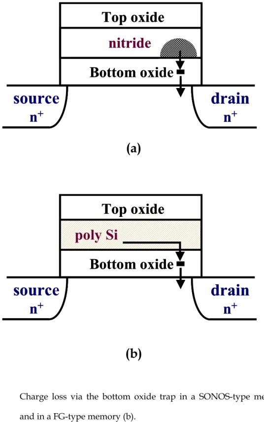
Flash memory has become a kind of nonvolatile memory widely used in personal computers (PCs) and electronic products, as it is capable of storing, reading and erasing data for many times, and the data stored therein will be retained even after the supplied power is cut off. Data in flash memory devices are usually stored in a multi-layer gate structure in a field effect transistor. With respect to charge storage devices, two state-of-the-art techniques are categorized. (a) Floating Gate Devices: Charge is stored in a thin conducting or semiconductor layer or conducting particles sandwiched between insulators [1.1]-[1.4]. Kahng and Sze proposed the first floating gate device in 1967 [1.5]. Storage of the charge in the floating gate allows the threshold voltage (Vt) to be electrically altered between a low and a high value to represent logic 1 and 0, respectively. (b) Charge Trapping Devices: Charge is stored in the traps at the interface of a multi-layer gate structure and/or in the bulk of insulator. The major difference in charge loss mechanisms between charge trapping and FG flash is that the charge storage media is non-conductive in charge trapping devices and is conducting in FG flash. In a charge trapping cell, only trapped charges near an oxide trap can leak directly, as demonstrated in Fig. 1.1(a). Trapped charges elsewhere cannot escape via oxide trap assisted tunneling directly since trapped charge cannot move. Those trapped electrons need to be excited to its conduction band and then move to the oxide trap and escape. In FG cells, since the storage media is conductive, stored electrons can move freely to the weak spot of the oxide and
escape by trap-assisted tunneling (Fig. 1.1(b)). This causes a limitation in the bottom oxide thickness and thus the channel length and the operating voltage cannot be scaled down further in FG flash. According to the device simulation, the channel length of NOR type floating gate flash memory cannot be scaled below 0.13µm, as shown in Fig. 1.2 [1.6]. In order to solve the dilemma, charge trapping device becomes an attractive solution. Ref. [1.7]-[1.10] indicated various candidates for trapping material. Among them, nitride-based material has been considered to be the most promising candidate for successfully integrated into standard logic process.
Fig. 1.3 illustrates the development of the nitride-based nonvolatile memory device. The early MNOS (Metal Nitride Oxide Silicon) [1.11][1.12] devices of the 1960s and mid-1970s were used an aluminum gate technology, relatively thick nitride (45nm), and thin tunnel oxides (2nm). In the latter 1970s and early 1980s, the technology moved into ploy-silicon gates SNOS (Silicon Nitride Oxide Semiconductor) [1.13][1.14] cells with reduced nitride thickness (25nm). Later, silicon-gate SONOS (Silicon Oxide Nitride Oxide Semiconductor) [1.15]-[1.17] devices was proposed in the mid-1980s and 1990. SONOS/MONOS provides the most promising structures with an additional top oxide. Holes are blocked from gate injection to the nitride as a result of its high barrier (3.9eV). Therefore, memory window is widened and nitride thickness can be scaled to around 5nm to 15nm. With the thinner effective thickness, SONOS/MONOS can be operated at lower voltage.
1.2 Uniform charge storage versus localized charge storage
Recently, considerable research efforts have been made to study nitride trap storage flash memories for its lower voltage operation, smaller cell size, simpler
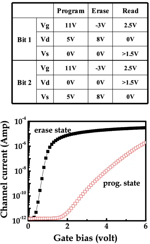
fabrication process, and no drain-induced turn-on [1.18]-[1.20]. These cells have generally categorized into two types; the first one utilizes uniform charge storage in a nitride layer, such as conventional SONOS/MONOS and the second one has localized charge storage at the source/drain junctions, such as NROM [1.19] or Nbit [1.21] technology. The operation principles between the two types are compared in Fig. 1.4. Among NROM or Nbit structure, attention is particularly paid to its two-bit storage capability. The two bits operation can be achieved by placing programmed charges in the nitride layer locally above the source or the drain junction by channel hot electron (CHE) program and band-to-band hot hole (BTB HH) erase. To allow for two-bit operation, the applied bit-line voltage in reverse-read must be sufficiently large (>1.5V) to be able to “read-through” the trapped charge in the neighboring bit. Table. 1.1 shows the operation biases for program, erase, and read, respectively. The IV characteristics of program state and erase state are shown in Fig. 1.5. A narrow charge trapping region, typically tens of nano-meter, deteriorates the sub-threshold swing in program state. Because of a thicker bottom oxide and the non-uniformity of charge stored in the nitride layer, the reliability issues in Nbit cell are quit different from that in conventional SONOS cell. Several concerns are believed to possibly hinder Nbit’s development. (a) Second bit effect is the inevitable outcome in two-bit operation [1.22]. It is related to the programming sequence and the P/E stress condition. At present, no effective way can mitigate this intrinsic effect. As a result, second bit effect may result in a serious scaling problem in this technology. (b) Although excellent intrinsic integrity is possessed, data loss is still a reliability concern after stress. In low-Vt state, Vt up-drift was reported by the bottom oxide hole tunneling [1.21]. Much effort has been devoted to alleviating the issue. For
example, a “soft hot electron injection” combined with a circuit judgment [1.23] is demonstrated to neutralize the positive hole charge. Reduction of the bottom thickness is another way to reduce the drift [1.24]. In high-Vt state, Vt loss was identified by Frenkel-Poole emission subsequently followed by oxide trap assisted tunneling [1.21]. The two-step charge loss closely relates to the bottom oxide robustness and/or the nitride trap energy deepness. Nitrided-oxide [1.25] or deuterium treatment [1.26] can better the bottom oxide quality. The ratio of SiH4 to
N2 during nitride film growth has a significant influence on trap energy distribution
[1.27]. Several groups have investigated the impact of trap energy on retention characteristics and attempted to extract the energy distribution [1.28], but some deficiencies and misunderstandings exist in their methodology. All previous literatures are work on the SONOS cell with an ultra-thin bottom oxide (1.5nm~2.5nm). They hypothesized the time through the bottom oxide can be ignored and the trapped charges are almost thermally activated in high temperatures (>85C). However, in such thicknesses, direct tunneling (DT) rather than thermal emission governs the charge loss mechanism even in these high temperatures. On the other side, for today’s SONOS cells, a thicker bottom oxide is usually employed, causing above hypothesis impractical. With a larger oxide thickness, more factors should be taken into account in a charge loss model. For example, a pronounced stress-induced oxide trap assisted leakage current is exhibited. In addition, charges re-trapping in silicon nitride are also significant [1.29]. This effect is complicated and necessitates a numerical technique for accurate modeling. (c) For Nbit cell, the read current fluctuation will be worsened due to the threshold voltage non-uniformity [1.30]. The design margin will be degraded and cause a failure, especially in
multi-level operation.
1.3 Organization of the Project
The scope of this project mainly focuses on reliability concerns of nitride-based storage memory, which are schematically illustrated in Fig. 1.6. Following the introduction, the mechanism of endurance degradation after P/E cycling stress in Nbit cells is described in Chapter 2. Proposed in Chapter 3 is a modified charge pumping technique for direct characterization of programmed charge lateral distribution in silicon nitride. P/E cycling stress induced programmed charge broadening effect is also investigated in this measurement. Various reliability issues including erase-Vt state threshold voltage instability, read-disturb, and high-Vt state charge loss are identified and the responsible models are made in Chapter 4. To further explore the charge loss mechanisms in high-Vt state, a numerical algorithm is established in Chapter 5. With the use of the numerical analysis, the influence of bottom oxide thickness and program/erase stress on charge retention is retrieved. An anomalous two-stage feature during retention measurement and the responsible origins are also discussed here. From the study in Chapter 5, a simple technique based on Frenkel-Poole emission to extract a silicon nitride trap density from stress induced nitride charge leakage current is developed in Chapter 6. Lateral threshold non-uniformity induced read current noise is verified in Chapter 7. A simple but reasonable model for read current distribution is proposed. Finally, conclusions are drawn in Chapter 8.
(a)
(b)
Fig. 1.1 Charge loss via the bottom oxide trap in a SONOS-type memory (a) and in a FG-type memory (b).
source
n
+
Top oxide
poly Si
Bottom oxide
drain
n
+
source
n
+
Top oxide
poly Si
Bottom oxide
drain
n
+
source
n
+
Top oxide
nitride
Bottom oxide
drain
n
+
source
n
+
Top oxide
nitride
Bottom oxide
drain
n
+
Fig. 1.2 Scaling limitation of NOR type floating gate flash. IDTO is drain induced
turn-on leakage current, IBBT is band-to-band tunneling current, tPGM
refers to the hot electron programming time, and IREAD is the current
needed for read. The shaded region refers to the design window. For the above design constraints, the design window will no longer exist when device channel length is below 0.13µm.
(a)
(b)
(c)
Fig. 1.4 Program & Erase operations in Nbit cells (a) and in SONOS cells (b). The operation modes are summarized in (c).
BTB HH
FN
Erase
CHE
FN
Program
2 bits/cell
1 bit/cell
NROM or Nbit
(>40Å)
Conventional SONOS
(15Å~35Å)
BTB HH
FN
Erase
CHE
FN
Program
2 bits/cell
1 bit/cell
NROM or Nbit
(>40Å)
Conventional SONOS
(15Å~35Å)
P-substrate
oxide
n
+n
+S
D
G
-FN +FNP-substrate
oxide
oxide
nitride
n
+n
+bit1
bit2
S
D
G
CHE BTB HHTable. 1.1 Bias conditions for Nbit two-bit operation.
Fig. 1.5 Channel current versus gate bias in erase state and in program state.
0V
8V
5V
Vs
>1.5V
0V
0V
Vd
2.5V
-3V
11V
Vg
Bit 2
>1.5V
0V
0V
Vs
0V
8V
5V
Vd
2.5V
-3V
11V
Vg
Bit 1
Read
Erase
Program
0V
8V
5V
Vs
>1.5V
0V
0V
Vd
2.5V
-3V
11V
Vg
Bit 2
>1.5V
0V
0V
Vs
0V
8V
5V
Vd
2.5V
-3V
11V
Vg
Bit 1
Read
Erase
Program
0
2
4
6
10
-1210
-1010
-810
-610
-4erase state
prog. state
C
h
an
ne
l curren
t (A
mp)
Gate bias (volt)
0
2
4
6
10
-1210
-1010
-810
-610
-4erase state
prog. state
C
h
an
ne
l curren
t (A
mp)
Fig. 1.6 The design margin for Nbit operation. RT RD Charge loss 2ndBit effect Sensing deficiency EM PM Vt,ini Vt,ini Vt,stress Vt,stress
Chapter 2
Chapter 3 Chapter 4
Chapter 4&5
Chapter 6
Chapter 7
RT RD Charge loss 2ndBit effect Sensing deficiency EM PM Vt,ini Vt,ini Vt,stress Vt,stressChapter 2
Chapter 3 Chapter 4
Chapter 4&5
Chapter 6
Chapter 7
Chapter 2
Program/Erase Cycling Induced Endurance Degradation in
Nbit Flash Memory Cell
2.1 Introduction
Endurance is an important issue in nonvolatile memory. It is defined by the number of data changes that can be performed in every cell of a given memory chip before one of the cells fails to meet the data sheet specifications. It describes the reliability of a device in terms of the number of program/erase (P/E) operations that can be performed on it without failure. Today, most commercially available nonvolatile memory products are guaranteed to withstand, at least 10,000 P/E cycles [2.1]. In a floating gate memory, electron trapping after numerous P/E cycles in tunnel oxide builds up a permanent negative charge, thereby reducing the electric field and injected tunneling current for the same applied terminal voltage. For a constant program voltage and program time, this reduces the program-state threshold voltage whereas increases the erase-state threshold voltage, resulting in a threshold voltage window closure problem [2.2]. In Nbit devices, the window closure is not observed (Fig. 2.1(a)). Instead, there appears an upward shift of both program-state and erase-state threshold voltages after P/E stress. We will discuss the cause for this endurance degradation in Nbit cells.
2.2 Endurance Failure in Nbit Cells
window with P/E cycles is due to trap generation in the tunnel oxide. Threshold voltage window opening in the initial tens of cycles is caused by positive charge trapping, whereas window closing after 104-105 cycles is caused by electron trapping
in the oxide (Fig. 2.1(b)) [2.3]. The Nbit cells apparently exhibit a different feature. Both program-state and erase-state threshold voltages move upward in parallel (Fig. 2.1(a)). This characteristic reveals that programming and erasing speeds are not degraded after cycling stress and implies that the failure of endurance may result from the aging of the tunnel oxide, including interface state creation [2.4] or oxide charge accumulation caused by cycling stress [2.5]. Interface state creation can be easily excluded since the sub-threshold swing in a 100k-P/E-cycled device is similar to that of the fresh one, no matter in program state or in erase state, as shown in Fig. 2.2. Based on the above observation, it seems that oxide trap/oxide charge creation should be responsible for the endurance failure.
2.3 Evidence of Negative Charge Creation
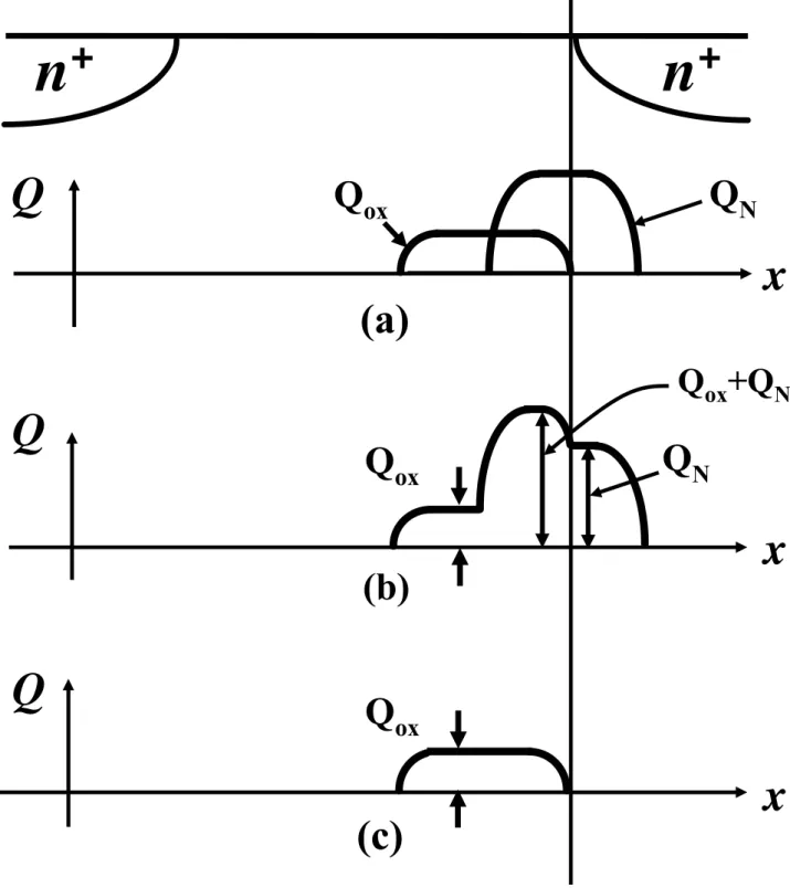
The sub-threshold characteristics at program state and erase state in a fresh device and in a cycled device are compared in Fig. 2.2. Although no significant swing degradation is observed, we do observe a parallel shift of the I-V curve before and after P/E stress. The parallel shift in Fig. 2.2 is usually attributed to negative trapped charge creation in the bottom oxide. Thus, the ONO dielectric layers actually consist of two kinds of charge in program state; negative trapped charge in the bottom oxide (QN) and negative charge in the nitride (Qox), as illustrated in Fig. 2.3. In erase state,
the nitride charge (QN) can be neutralized by band-to-band hot hole injection
in the bottom oxide. Fig. 2.3 is a diagram illustrating the charge distribution in the ONO in program state (Fig. 2.3(b)) and in erase state (Fig. 2.3(c)). Qoxis negligible in a fresh device and increases with P/E stress. The build-up of the bottom oxide charge Qox, which cannot be removed by erase, explains the upward shift of the threshold window with P/E cycles.
The relative positions of Qox and QN depicted in Fig. 2.3 are constructed by the
following measurements. A fresh device and a 100k cycling stressed device are used for this study. GIDL current and threshold voltage are measured. GIDL current is used as a monitor for the charge in the ONO layers above the n+ drain region while threshold voltage can be used to measure the ONO charge in the channel region (please refer to Fig. 2.4(a)) [2.6]. First, we adjust the programming bias condition for each device to make sure that program-state GIDL current is the same in each device. The measured program-state threshold voltage is 4.13V in the fresh device and 4.62V in the 100k device. The same GIDL current means the two devices have the same amount of charge above the n+ drain. The higher threshold in the 100k cell is believed
due to the additional stress created oxide charge Qox. Then, the erase characteristics
of the two devices are measured. Fig. 2.4(b) shows the threshold voltage shift with erase time in the two devices. It is interesting to note that the two curves in Fig. 2.4(b) are almost identical. Two questions are brought about. First, why the two devices have the same erasing speed? This can be understood because the two devices have the same GIDL current. The readers should be reminded that GIDL reflects the strength of hot hole erasing. Second, why the erasing in the 100k cell stops around 1millisecond and the threshold voltage shift is the same as in the fresh cell although the program-state threshold in the 100k device is about 0.5V higher? This implies that
part of the ONO charge in the 100k device, amounting to 0.5V threshold voltage shift, cannot be erased. Why this charge cannot be erased? What kind of charge is it? We believe the answer is oxide trapped charge Qox. From the above arguments, the picture of the oxide charge and the nitride charge distributions in the 100k device is constructed as in Fig. 2.4(b).
In the second experiment, both the devices are programmed to have the same threshold voltage. The measured GIDL current in the 100k device is found to be smaller than that in the fresh device. Fig. 2.5(a) shows the measured result and the corresponding charge distributions. Again, the threshold voltage shift versus erase time in the devices is measured (Fig. 2.5(b)). Now, the fresh device has a larger threshold shift. Our explanation is as follows. Although the total ONO charge in the channel region in the two devices are equal (i.e. the same program-state threshold), the ONO charge in the fresh cell is completely the erasable nitride charge and thus the threshold voltage shift in the fresh device during erase is larger.
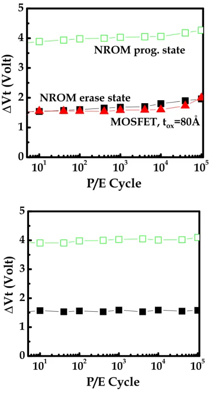
Finally, we would like to compare the P/E stress effects in the conventional gate MOSFET and in the Nbit cell. Fig. 2.6(a) shows the ∆Vt in the MOSFET and in the Nbit cell. Since oxide charge creation is the only cause for the shift in the nMOSFET, the similarity between the NMOSFET and the Nbit in Fig. 2.6(a) indicates that solely oxide charge creation can explain the observed endurance degradation in the Nbit cell
2.4 Improvement of Cycling Endurance
From the above study, we conclude that the shift of the threshold voltage window in the Nbit cell is attributed to bottom oxide charge creation. The endurance
of the operation window can be improved by increasing bottom oxide robustness. It has been well reported in literature that thinner oxide has less charge creation [2.7]. The reduction of bottom oxide thickness should be an effective approach to improving the endurance. Another approach is to strengthen the erase bias condition. A stronger erase will result in accumulation of excess holes in the nitride to compensate for the negative oxide charge or even increases the possibility of recombination of injected hot holes and oxide trapped electrons.
Fig. 2.6(b) shows the threshold voltage window by using a stronger erase bias. Endurance up to 106 cycles can be achieved.
Fig. 2.1 (a) Endurance characteristics of a Nbit cell operation window. Program bias is Vg/Vd=11V/4.7V, 10µs and erase bias is Vg/Vd=-3V/, 3ms. The thickness of each ONO layer is 7nm, 6nm and 6nm. (b) Endurance characteristics of a floating-gate flash cell showing the window opening and closing.
10
010
110
210
310
410
50
2
4
6
8
10
P/E Cycle
Vt
(Vo
lts
)
10
010
110
210
310
410
50
1
2
3
4
5
P/E Cycle
V
t
(Vol
ts)
(a)
(b)
Fig. 2.2 Nbit cell subthreshold charcateristics in erase state and in program state before stress and after 100k cycling stress. QN and Qox represent the
charge created by P/E stress and the injected charge by programming, respectively.
0
1
2
3
4
5
10
-13
10
-11
10
-9
10
-7
10
-5
10
-3
Q
ox
Q
N
+Q
ox
Q
N
Gate Bias (Volt)
Cha
nnel
cur
rent
(A
m
p
)
Fig. 2.3 (a) The relative position of Qox and QN in a cycled cell. The x-axis is the
channel direction. There is an overlap between Qox and QN. (b) The
charge distribution of Qox and QN in program state after cycling stress.
(c) Qox in erase state in a stressed cell.
x
Q
Q
ox
Q
N
x
Q
Q
ox
Q
N
Q
ox
+Q
N
x
Q
Q
ox
n
+
n
+
(a)
(b)
(c)
(a)
(b)
Fig. 2.4 (a) Illustration of the charge distribution in the fresh and the 100k P/E devices. The two devices are programmed to have the same GIDL current. (b) Threshold voltage shift with erase time in a fresh cell and in a 100k cycled cell.
10
010
110
210
310
40.0
0.5
1.0
1.5
2.0
fresh
100k P/E
Erase time (ms)
∆Vt
(V
olt)
PE 100k
fresh
Q
Nx
Q
Vt GIDL
Q
ox(a)
(b)
Fig. 2.5 (a) Illustration of the charge distribution in the fresh and 100k P/E devices. The two devices are programmed to have the same threshold voltage. (b) The erase characteristics in the fresh and in the 100k P/E devices. The two devices have the same program - state threshold voltage.
10
110
210
310
40.0
0.5
1.0
1.5
2.0
Q
SiNQ
oxfresh
P/E 100k
Erase time (ms)
∆Vt
(V
ol
t)
Q
NPE 100k
fresh
x
Q
Vt GIDL
Fig. 2.6 (a) Threshold voltage variation versus P/E cycle number in a conventional gate MOSFET and in a Nbit. (b) Threshold voltage versus P/E cycle number in a Nbit cell with a stronger erase bias.
10
110
210
310
410
50
1
2
3
4
5
NROM prog. state
NROM erase state
MOSFET, t
ox=80Å
P/E Cycle
∆Vt
(V
olt)
10
110
210
310
410
50
1
2
3
4
5
P/E Cycle
∆Vt
(V
ol
t)
Chapter 3
Characterization of Programmed Charge Lateral Distribution
in Nbit Flash Memory Cell by Using Charge Pumping
Technique
3.1 Introduction
In two-bit operation, the control of programmed charge lateral distribution of each bit is a major concern for the scalability of the Nbit cell. The stored electrons at the first bit will affect the threshold voltage of the second bit in reverse read and vice versa. This phenomenon is referred to as the second bit effect [3.1] and is closely related to programmed charge lateral spread. Furthermore, the lateral spread of stored charges in nitride will result in the degradation of erase capability or erase speed due to a spatial mismatch between stored electrons and injected holes during erase [4.2]. For these reasons, comprehensive understanding of programmed charge spatial distribution is of vital importance in the optimization of the cell structure and operation bias.
Attempts have been made in the past to characterize the trapped charge distribution in a Nbit cell [3.3][3.4]. Larcher et al. used an inverse modeling approach to extract programmed charge distribution from measured I-V characteristics [3.3]. This method, however, suffers from some drawbacks, such as lack of precise information on device doping profile and extensive numerical calculation to reach a consistent solution between stored charge distribution and measurement result.
the lateral distribution of programmed charges at the source and drain junctions separately without using computer simulation. The devices and measurement setup throughout this study will be described. The charge pumping current for single bit storage and two-bit storage will be demonstrated. Program/erase cycling stress effect on stored charge distribution will be also examined.
3.2 Device Structure and Measurement Setup
The nitride flash cells used in this work have a gate length of 0.5µm and a gate width of 1.0µm. The thickness of each ONO layer is 9nm (top oxide), 6nm (nitride) and 6nm (bottom oxide). The cell intrinsic threshold voltage (Vt) is about 1.6V where Vt is defined as the gate voltage when the drain current is 1µA at a reverse read voltage of 1.6V. Channel hot electron program and band-to-band hot hole erase accompanied by a reverse read scheme are adopted to achieve two-bit per cell operation.
In charge pumping (CP) measurement, the voltage waveforms at gate and drain terminals supplied by a two-channel pulse generator are illustrated in Fig. 3.1. The employment of a dual-channel pulse generator can circumvent the misalignment of gate and drain signal. The gate pulse has a fixed high level (Vgh) and a variable low level (Vgl). The Vgh is sufficiently high (Vgh=6V here) to ensure that the entire channel at program state is inverted.
The charge pumping current, named hereafter Icp, is measured at the substrate. To probe the lateral extent of programmed charge in the drain side (or the source side), Vd (or Vs) is adjusted to modulate the drain (or source) depletion width while Vs (or Vd) is left floating. In this way, there is no channel current and thus no impact
ionization induced substrate current in CP measurement. Besides, the Vd is 180o
phase-shifted with respect to Vg so that the drain signal is applied only during the interface-trap (Nit) electron emptying period. Because the length of the channel hot electron injection region (i.e., programmed region) is only about a few nanometers [3.6], Icp contributed by interface traps in the programmed region is very low and close to the measurement limit of the current setup. Therefore, a higher frequency of 2.5MHz with 50% duty cycle and rise/fall times of 15ns each is selected in CP measurement. To make sure the measured Icp is still reliable at this frequency, the frequency dependence of normalized charge pumping current at program state is shown in Fig. 3.2. The constant Icp/f confirms the validity of the CP measurement.
3.3 Measurement Result and Discussion
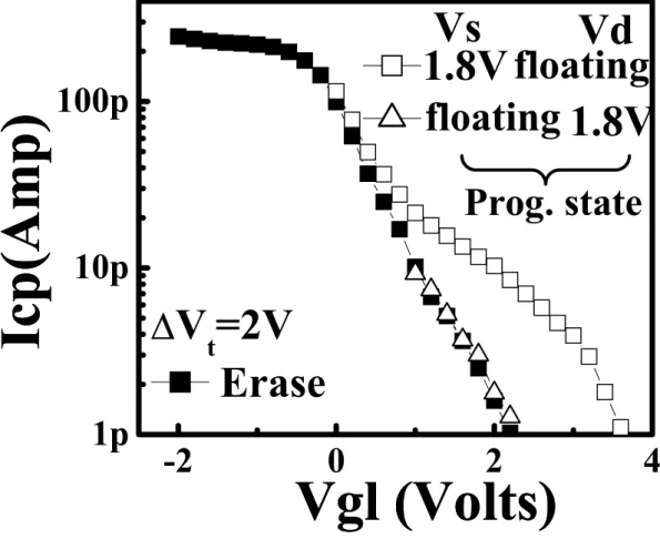
3.3.1 Single-bit StorageFig. 3.3 shows the Icp versus Vgl curves in a virgin cell, after programming only, and after one P/E cycle, respectively. Only the first bit (drain side) is P/E cycled and the Vd in CP measurement is 0V. The threshold voltage window (∆Vt) is 2V. The Icp in a virgin cell and in erase state are almost identical, whereas a noticeable Icp bump at program state is noticed. This Icp bump is attributed to a local increase of channel threshold voltage due to negative nitride charge trapping. To verify the nitride charge storage effect, the Icp characteristics for two different threshold voltage windows, ∆Vt=2V and 2.7V, are compared in Fig. 3.4. As expected, the larger threshold voltage window exhibits a larger Icp bump due to more stored electrons. The dependence of the program-state Icp bump on Vd in charge pumping measurement is shown in Fig. 3.5. The Icp bump is suppressed as Vd increases. The
reason is that the drain depletion region increases with Vd. At a sufficiently large Vd (in this figure 1.8V), interface traps underneath the program charges are completely “masked” by the drain depletion region. Thus, these interface traps can no longer go through inversion-accumulation cycles in CP measurement and do not contribute to Icp. As a result, the program-state Icp bump is totally suppressed. Our result here implies that a Vd about 1.8V is necessary in reverse read to avoid completely the second bit effect. In contrast, when Vs is applied in CP measurement, the Icp bump is not affected at all (Fig. 3.6). This indicates that programmed charge is highly localized near the drain edge.
3.3.2 Two-bit Storage
The Nbit cell stores two bits at different locations (drain-side and source-side). Each bit within a cell serves as binary unit of data that is totally mapped to four states in a memory cell. The Icp of the four states corresponding to “11”, “10”, “01” and “00” are shown in Fig. 3.7. “00” denotes both bits in program state. “10” (or “01”) denotes the drain-side bit in erase state (or in program state) and the source-side bit in program state (or in erase state). To explore the influence of the programming sequence on trapped charge spatial profile, the charge pumping measurement is performed after each bit is programmed. Fig. 3.8 shows the Icp of the first programmed bit and the second programmed bit, respectively. Here, the Icp of the second programmed bit is obtained in two ways. One is to measure Icp after the first bit is erased. The second approach is to subtract the fist bit Icp from the “00” state Icp. Fig. 3.9 compares the second bit Icp from the above two approaches and the result is almost the same. It should be emphasized that a crossover of the first bit and the
second bit Icp in Fig. 3.8 is observed. This suggests that the second programmed bit has a wider charge distribution but a smaller peak density. The reason will be discussed later. To profile the nitride stored charge lateral distribution, a technique similar to [3.6] is performed. In profiling, we make the following assumptions. First, we assume that a fresh cell has uniform interface trap density (Nit) along the channel [3.6]. The charge pumping current thus should have a linear dependence on channel position x; L I ) V ( I x max , cp gl cp = (3-1)
where x=0 is defined at the edge of the source or drain junction. L is the channel length and Icp,max denotes the saturated charge pumping current. The second assumption is that Nit generation after one program/erase cycle is negligible. Based on these assumptions, the nitride charge distribution is deduced as follows,
) V V ( q C ) x ( QN = ONO gl− ti (3-2)
where QN(x) is the nitride charge density at the position x, and Vti stands for the
threshold voltage of a fresh device. Fig. 3.10 depicts the extracted stored charge distribution of the first programmed bit and the second programmed bit versus a distance from the source/drain junction. The stored charges extend into the channel about tens of nanometers. This result is in agreement with the simulation in [3.3]. In addition, the CP measurement result shows that the second programmed bit exhibits
a broader distribution but a smaller peak density. To explain this result, a two-dimensional device simulation is performed. A rectangular charge distribution with a width of 30nm and a charge density of 1.6x1019 cm-3 is used. Fig. 3.11 shows
the lateral channel electric field distribution in the second bit programming. A large channel field exists not only in the programmed region but also in the first bit region (drain side). Such a large field in the first bit region will accelerate channel electrons from the drain and cause earlier hot electron injection into the nitride, thus resulting in a broader second bit distribution. Finally, we would like to remark that Eq. (3-2) and consequently Fig. 3.10 are derived from a simplified one-dimensional model. For a narrow charge distribution by hot electron programming, Eq. (3-2) only serves as a first-order approximation. Accurate profiling of programmed charge distribution requires a more complicated 2D model.
The programmed charge lateral extent can be also probed by varying Vd (or Vs) in CP measurement. Fig. 3.12 shows the difference in Icp between program state and erase state versus Vd (or Vs). ∆Icp is measured at Vgl=1.6V. The 2nd programmed bit needs a larger junction bias to“mask” the programmed charge. The same conclusion that the second bit has a broader charge distribution is obtained.
3.3.3 P/E Cycling Stress Effect
The P/E cycling stress effect on programmed charge distribution is examined in Fig. 3.13 by using the variable Vd method. The Vt window keeps the same during cycling. Again, the ∆Icp is measured at Vgl=1.6V and is normalized to its value at Vd=0V to compensate for interface trap creation effect for different cycling stress. It has been reported that hot-carrier stress created oxide traps spread toward the
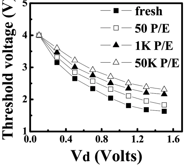
channel with stress time [3.7][3.8]. Such traps, especially positively charged traps, can effectively lower the Si/SiO2 injection barrier [3.9][3.10] and enhance the electron injection probability. Therefore, as cycle number (stress time) increases, the hot electron injection region expands toward the channel due to the spread of the bottom oxide damaged region. A larger Vd in CP measurement is necessary to screen programmed charge at a larger cycle number. The consequence of the broadening of programmed charge distribution is the degradation of the second bit effect. Fig. 3.14 shows the threshold voltage versus Vd in reverse read for different cycle numbers. The second bit effect is apparently worsened with increasing cycle number.
3.4 Summary
We have characterized the programmed charge lateral distribution in a two-bit storage nitride flash cell by channel hot electron program. The charge pumping measurement reveals that the charge distribution of each bit extends into the channel for tens of nanometers. This suggests the possibility of further scaling down the nitride flash cell with respect to the concern of the overlap of two bit charges. Our study also shows that the charge distribution of the secondly programmed bit is influenced by the stored charge of the first bit. A broader second bit charge distribution is obtained.
Fig. 3.1 (a) Schematic diagram of a two-bit storage nitride flash cell and (b) charge pumping measurement waveform. The dashed line in the substrate represents the depletion region caused by Vd. The thickness of the ONO gate stack is 9nm (top oxide), 6nm and 6nm, respectively.
Vd
Vg
V
gh
V
gl
0
(b)
P-substrate
oxide
oxide
nitride
n
+n
+floating
V
d
I
B= I
cp
V
g
P-substrate
oxide
oxide
nitride
n
+n
+floating
V
d
I
B= I
cp
V
g
(a)
Fig. 3.2 The dependence of normalized charge pumping current (Icp/f) on measurement frequency. In charge pumping measurement, the Vt window (∆Vt) is 2.7V and Icp is measured at Vgl=2.5V.
1.0
1.5
2.0
2.5
1.00
1.25
1.50
1.75
Frequency (MHz)
Icp/f
(1
0
-1
7
C)
Prog. state
∆V
t
=2.7V
Fig. 3.3 Icp versus Vgl in a fresh cell, in program-state and in erase state, respectively. The Vt window (∆Vt) is 2V. Vd in CP measurement is 0V.
-2
0
2
4
1p
10p
100p
fresh
Prog. state
Erase state
Vgl(Volts)
Icp(A
m
p)
Vgl(Volts)
Icp(A
m
p)
nitride charge
trapping
Fig. 3.4 Icp versus Vgl for different Vt window. The program-state Icp bump increases with Vt window due to more injected charges.
-2
0
2
4
1p
10p
100p
Erase
Prog. state
∆V
t
=2.7V
∆V
t
=2V
V
gl
(Volts)
I
cp
(A
m
p
)
-2
0
2
4
1p
10p
100p
Erase
Prog. state
∆V
t
=2.7V
∆V
t
=2V
-2
0
2
4
1p
10p
100p
Erase
Prog. state
∆V
t
=2.7V
∆V
t
=2V
V
gl
(Volts)
I
cp
(A
m
p
)
Fig. 3.5 Icp versus Vgl with different Vd in CP measurement. The program-state Icp bump decreases with Vd. The Vt window is 2V.
-2
0
2
4
1p
10p
100p
0V
0.8V
1.8V
Erase
Vgl (Volts)
Icp
(A
m
p)
∆V
t
=2V
V
d
Prog.
state
-2
0
2
4
1p
10p
100p
0V
0.8V
1.8V
Erase
Vgl (Volts)
Icp
(A
m
p)
∆V
t
=2V
V
d
-2
0
2
4
1p
10p
100p
0V
0.8V
1.8V
Erase
Vgl (Volts)
Icp
(A
m
p)
Vgl (Volts)
Icp
(A
m
p)
∆V
t
=2V
V
d
Prog.
state
Fig. 3.6 The program state Icp measured at Vd=1.8V & Vs floating and at Vs=1.8V and Vd floating.
-2
0
2
4
1p
10p
100p
Vd
Vs
1.8V
floating
floating
1.8V
∆
V
t
=2V
Erase
Vgl (Volts)
Icp(A
mp)
Vgl (Volts)
Icp(A
mp)
Prog. state
Fig. 3.7 The Icp versus Vgl of the four states of two-bit storage. “11” represents both bits in erase-state and “10” represents one bit in erase-state and one bit in program-state.
-2
0
2
4
1p
10p
100p
"00"
"01"&"10"
"11"
V
gl
(Volts)
I
cp
(A
m
p
)
∆V
t
=2V
Fig. 3.8 Comparison of the Icp versus Vgl of the first programmed bit and the secondly programmed bit. The 2nd bit Icp is measured with the first bit erased.
-2
0
2
4
1p
10p
100p
Vgl (Volts)
Icp
(A
m
p)
∆V
t
=2V
1st prog. bit
2nd prog. bit
“cross-over”
-2
0
2
4
1p
10p
100p
Vgl (Volts)
Icp
(A
m
p)
∆V
t
=2V
1st prog. bit
2nd prog. bit
“cross-over”
-2
0
2
4
1p
10p
100p
Vgl (Volts)
Icp
(A
m
p)
Vgl (Volts)
Icp
(A
m
p)
∆V
t
=2V
1st prog. bit
2nd prog. bit
“cross-over”
Fig. 3.9 Comparison of the second bit Icp-Vgl from two approaches. One is to measure Icp after the first bit is erased. The second approach is to subtract the fist bit Icp from the “00” state Icp.
-2
0
2
4
1p
10p
100p
1st bit erased
Vgl (Volts)
Icp
(A
m
p)
Erase
subtraction
from “00” state
-2
0
2
4
1p
10p
100p
1st bit erased
Vgl (Volts)
Icp
(A
m
p)
Vgl (Volts)
Icp
(A
m
p)
Erase
subtraction
from “00” state
Fig. 3.10 Lateral profiling of the programmed charge distribution of the first programmed bit and the secondly programmed bit. A uniform interface trap distribution along the channel is assumed. Icp,max in Eq. (3-1) is 195pA.
0.00
0.01
0.02
0.03
0.04
0.0
5.0x10
121.0x10
131st prog. bit
2nd prog. bit
“cross-over”
Q
N
/q
(c
m
-2
)
Distance (
µm)
0.00
0.01
0.02
0.03
0.04
0.0
5.0x10
121.0x10
131st prog. bit
2nd prog. bit
“cross-over”
0.00
0.01
0.02
0.03
0.04
0.0
5.0x10
121.0x10
131st prog. bit
2nd prog. bit
“cross-over”
Q
N
/q
(c
m
-2
)
Distance (
µm)
Fig. 3.11 Simulated channel field distribution in 2nd bit programming from 2D device simulation. x=0 is at the n+ source edge and x=0.4 is at the n+
drain edge. Vs=6.5V and Vg=11 in 2nd bit programming.
0.0
0.1
0.2
0.3
0.4
0.0
2.0x10
54.0x10
56.0x10
5Distance (
µm)
C
h
an
n
el
f
iel
d
(V
/cm
)
Fig. 3.12 The difference in Icp between program-state and erase-state as a function of drain bias for the 1st bit and source bias for the 2nd bit. The ∆cp is obtained from Fig. 3.7 and Fig. 3.8 at Vgl=1.6V.
0.0
0.5
1.0
1.5
2.0
0.0
5.0p
10.0p
15.0p
20.0p
1st prog.bit
2nd prog. bit
∆
Icp
(A
m
p
)
Applied junction bias (Volts)
0.0
0.5
1.0
1.5
2.0
0.0
5.0p
10.0p
15.0p
20.0p
1st prog.bit
2nd prog. bit
∆
Icp
(A
m
p
)
Fig. 3.13 The difference in Icp between program state and erase state as a function of Vd in CP measurement at various P/E cycle numbers. ∆Icp is measured at Vgl=1.6V and is normalized to its value at Vd=0V to take into account interface trap creation in cycling.
0.0
0.5
1.0
1.5
2.0
0.0
0.5
1.0
fresh
50 P/E
1K P/E
50K P/E
V
d
(Volts)
Nor
m
al
iz
ed
∆
Icp
(Am
p)
Fig. 3.14 Threshold voltage versus reverse read Vd for different cycle numbers.
0.0
0.4
0.8
1.2
1.6
1
2
3
4
5
fresh
50 P/E
1K P/E
50K P/E
V
d
(Volts)
Threshold voltage
(V)
0.0
0.4
0.8
1.2
1.6
1
2
3
4
5
fresh
50 P/E
1K P/E
50K P/E
V
d
(Volts)
Threshold voltage
(V)
Chapter 4
Reliability Mechanisms of Data Retention and Read-Disturb
in Nbit Flash Memory Cells
4.1 Introduction
The major advantages of the Nbit cell, as compared with the conventional SONOS flash EEPROM, has a better retentivity due to a thick bottom oxide thickness [4.1]. The bottom oxide in the Nbit cell is normally thicker than 40Å. Such oxide is sufficiently thick to avoid charge direct tunneling [4.2]. The Nbit cell exhibits no window loss before P/E cycling. However, after P/E cycled stress, the retentivity behavior is degraded, showing a window closure with time (Fig. 4.1). As previously stated, the retention loss characteristics are determined by two factors. (a) oxide charge (Qox) de-trapping in erase state [4.3], strongly dependent on P/E stress and oxide quality [4.4], and (b) nitride charge (QN) loss in program state [4.5], closely related to temperature and electric field.
In this chapter, the reliability issues of the Nbit flash cell including low-Vt state threshold voltage instability (room temperature threshold voltage drift, RT drift), read-disturb, and high-Vt state charge loss will be reviewed. Responsible mechanisms and possible solution will be discussed.
4.2 Room-Temperature Threshold Voltage Drift
In a P/E stressed cell, the erase-state threshold is found to possess a positive drift with storage time (Fig. 4.1). This retention loss exhibits logarithmic
time-dependence but weak temperature dependence (Fig. 4.2). This is why the drift is referred to as RT drift [4.6]. Unlike a SONOS cell, the bottom oxide is sufficiently thick and thus this drift cannot be explained by nitride hole back tunneling [4.7]. Furthermore, we find that the Vt drift exhibits a peak around 10k P/E cycles in Fig. 4.3. To understand this peculiar cycle number dependence, the readers should be reminded that it is well published in literature that positive trapped charge creation is dominant in tunnel oxide in the initial period of P/E stress [4.8]. The appearance of the peak gives a clue that the Vt drift is related to positive charge creation in the bottom oxide. To explore the origin of the RT drift, Vt and GIDL techniques are used to monitor the charge, as shown in Fig.4.4 (a) and Fig.4.4 (b). From the change of Vt and GIDL, it can be deduced that after P/E stress the net ONO charge above the n+
region is positive and the net ONO charge above the channel region is negative. More exactly speaking, the ONO charge in the channel region comprises positive oxide charge (Qox) and negative nitride charge (QN). In storage, trapped holes in the
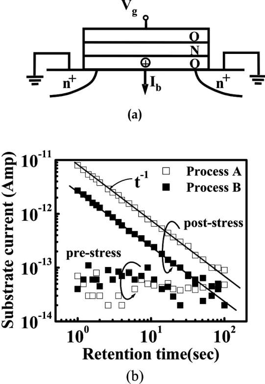
bottom oxide (Qox) can escape to the Si substrate with time. The total ONO charge in the channel region therefore becomes more negative and thus threshold voltage increases with time. To measure positive oxide charge de-trapping directly, the charge separation technique (Fig. 4.5(a)) is employed in large area devices with two different ONO processes (A and B). Process B is known to have a thinner bottom oxide, thereby causing a smaller Qox. The substrate current (Ib) before and after FN stress was measured in these two samples, as shown in Fig. 4.5(b). According to the hole tunneling front model [4.9], the post-stress substrate current resulting from positive oxide charge de-trapping follows a 1/t time-dependence,