國
立
交
通
大
學
電控工程研究所
碩
士
論
文
雜訊相依模型與模組設計最佳化運用在
離散時間積分三角類比數位轉換器
Noise Correlation Model and Model-based Design Optimization for
Discrete-Time Sigma-Delta Modulators
研 究 生:盛子恩
指導教授:陳福川 教授
雜訊相依模型與模組最佳化運用
在離散時間積分三角類比數位轉換器
Noise Correlation Model and Model-based Design Optimization for
Discrete-Time Sigma-Delta Modulators
研 究 生:盛子恩 Student:Tzu-En Sheng
指導教授:陳福川 Advisor:Fu-Chuang Chen
國 立 交 通 大 學
電 控 工 程 研 究 所
碩 士 論 文
A ThesisSubmitted to Department of Electrical and Control Engineering College of Electrical Engineering and Computer Science
National Chiao Tung University in partial Fulfillment of the Requirements
for the Degree of Master
in
Electrical and Control Engineering
September2010
Hsinchu, Taiwan, Republic of China
雜訊相依模型與模組最佳化運用在離散時間積分三
角類比數位轉換器
研究生:盛子恩 指導教授:陳福川 教授 國立交通大學 電控工程研究所摘要
傳統高階積分三角調變器的設計上,主要是依賴行為模擬的方法。然而此方法相 當耗時。本論文是第一個提出使用模組化設計的方法去設計積分三角調變器。在速度 上,使用模組化設計的方法將會比使用行為模擬的方法快上萬倍。由於先前非理想雜 訊以及失真模型的不完備,模組化設計的方法一直無法真正的去實現。如今,由於積 分器充放電雜訊模型以及放大器非線性直流增益諧波失真模型的推出,使得模組化設 計方法得以實現。然而,使用模組化設計方法將會遭遇到雜訊相依的問題;本論文將 會提出雜訊相依模型以便解決這個問題。除此之外,本論文也同時提出了積分三角調 變器最佳化設計流程。對照於一篇積分三角調變器設計實例,模組化積分三角調變器 最佳化設計將可以使用更短的時間去達到更高的訊號對雜訊以及失真比,同時降低積 分三角調變器的功率消耗。Noise Correlation Model and Model-based
Design Optimization for Discrete-Time
Sigma-Delta Modulators
Student:Tzu-En Sheng Advisor:Dr. Fu-Chuang Chen
Institute of Electrical and Control Engineering Nation Chiao Tung University
ABSTRACT
The conventional high-level SDM synthesis is mainly based on behavior simulation which is very time-consuming. This thesis is the first one in the literature to propose model-based SDM synthesis. Model-based method can be at the order of 104
times faster than simulation-based method, but it is never realized before due to the incompleteness of non-ideality models. The recent establishment of settling noise model [18] and OTA distortion model [17] facilitates model-based SDM designs. Nonetheless, new problem associated with model-based method arises, notably correlation between noises. Noise correlation models here are derived. In addition, a SDM design optimization scheme is proposed, which incorporates a comprehensive power consumption model. This model-based optimization is tested against a published SDM design, achieving higher SNDR and lower power results in a much shorter design time.
誌謝 Acknowledgment
我要將此論文獻給 我親愛的母親-許錦碧 女士 最疼我的父親-盛景徽 先生 若沒有他們,我不可能有機會完成此篇論文,並且從交通大學碩士班畢業。除此 之外,必須感謝指導教授陳福川博士兩年來嚴格的督促與指導,讓我學會做研究的方 法與心態。另外,也要感謝口試委員廖德誠教授、趙昌博教授與洪浩喬教授對本篇論 文所給予的建議與指導。 還要感謝實驗室學長智隆在我一年級時幫我打好深厚的研究基礎。感謝實驗室同 學嘉昌和學弟瑋才、國政和揚程陪我度過最後的學生生涯,並在研究上給予我很多幫 助。最後要謝謝這兩年在新竹唸書期間所有幫助過我的人,雖然無法一一列舉,但在 這邊向大家致上最大的謝意。Contents
中文摘要... I English Abstract... II Acknowledgment... III
Contents... IV Lists of Tables... VII Lists of Figures... VIII List of Symbols…... IX
Chapter 1 Introduction... 1
1.1 Current Status and Background... 1
1.2 Motivation and Aims... 1
1.3 Organization... 3
Chapter 2 SDM Noise Power and Distortion Power Models…... 4
2.1 Switch Non-idealities... 5
2.1.1 Switch Thermal Noise Power Model... 5
2.1.2 Nonlinear Switch on-resistance Distortion Power Model... 5
2.1.3 Clock-Feedthrough... 5
2.1.4 Charge Injection... 5
2.2 Capacitors Non-idealities... 6
2.2.1 Capacitor Mismatch Noise Power Model... 6
2.2.2 Capacitor Nonlinearity Distortion Power Model... 6
2.3 Finite and Nonlinear DC-gain... 6
2.3.1 Finite DC-gain Noise Power Model... 6
2.3.2 Nonlinear DC-gain Distortion Power Model... 6
2.4.1 Settling Noise Power Model... 6
2.4.2 Slew-Rate Distortion Power Model... 6
2.5 OTA Noise... 7
2.5.1 OTA Thermal Noise Power Model... 7
2.5.2 Flicker Noise Power Model... 7
2.5.3 Reference Circuit Noise Power Model... 7
2.6 Clock Jitter Effect... 7
2.7 Comparator Hysteresis... 7
2.8 Multi-Bit DAC Non-idealities... 8
2.8.1 DAC Noise Power Model... 8
2.8.2 DAC Distortion Power Model... 8
Chapter 3 SNDR Generation in Model-Based SDM Designs... 9
Chapter 4 Advantage of Model-Based SDM Designs... 17
4.1 SNDR Speed Comparison... 17
4.2 SDM Design Guide... 21
Chapter 5 Models of SDM Power Consumption... 23
5.1 Analog Power Consumption... 23
5.1.1 OTA Power Consumption... 23
5.1.2 Quantizer Power Consumption... 30
5.2 Digital Power Consumption... 30
5.2.1 DAC Power Consumption... 30
5.2.2 Switch Power Consumption... 31
5.2.3 DWA Power Consumption... 31
Chapter 6 Model-Based SDM Design Optimization... 35
6.1 Design Optimization Schemes... 35
6.1.2 SNDR and POWER Computation... 35
6.1.3 Cost Function Generation... 35
6.2 ΣΔ ADC for ADSL-CO Applications... 36
Chapter 7 Conclusions and Future Works... 39
Appendix... 40
Lists of Tables
TABLE 4.1: Running time of each non-ideality for both design approaches... 18
TABLE 5.1: Specific value of CD,eq for different bit number... 33
TABLE 6.1: Comparisons of our design results with those in [3]... 37
TABLE 6.2: The corresponding noise and distortion power for both designs... 37
Lists of Figures
Fig. 2.1: Schematic of SC single-loop 2nd-order SDM... 4
Fig. 3.1: Block diagram of single-loop 2nd-order SDM... 10
Fig. 3.2: The magnitude and angle of VModified_quantization_noise(f)... 12
Fig. 3.3: The magnitude and angle of VE(f)... 13
Fig. 3.4: Correlation powers (a) assumption that VE in negligible... 15
(b) assumption that VE exists... 15
Fig. 3.5: Each noise power w.r.t different SR values... 16
Fig. 4.1: Single-loop 2nd-order SDM model with relevant non-ideality blocks... 18
Fig. 4.2: The pie chart of SNDR computation time in model-based SDM design method... 19
Fig. 4.3: The pie chart of SNDR computation time in modified model-based SDM design method... 21
Fig. 5.1: OTA model... 23
Fig. 5.2: Integrator model with parasitic capacitor... 24
Fig. 5.3: (a) Telescopic OTA... 26
(b) Fold-Cascode OTA... 27
(c) Two-stage Miller-compensated OTA... 28
Fig. 5.4: Block diagram of DWA implementation...31
Fig. 5.5: 2 bit thermometer-to-binary ROM encoder... 32
Fig. 5.6: (a) 2-bit DWA power... 33
(b) 3-bit DWA power... 33
(c) 4-bit DWA power... 34
List of Symbols
Symbols
Physical
K Boltzmann’s constant T Absolute temperatureDefinitions
σcap Standard deviation of unit capacitance
σjit Standard deviation of clock jitter
ai Gain coefficient of i th integrator
A0 OTA finite DC-gain
Ain Amplitude of input signal
B Number of bits in the quantizer CC Compensation capacitor
CD,eq DWA equivalent capacitor
CI Integrating capacitor
CL OTA Load capacitor
CS Sampling capacitor
CSwitch Switch parasitic capacitor
Cu Unit feedback capacitor
Erf Error function f Feedback factor fB Signal bandwidth
fin Input signal frequency
fS Sampling Frequency
gm OTA transconductance
n Order of the sigma-delta modulator N Quantizer levels
RSwitch Switch on-resistance
VLSB Quantizer step size
VOS OTA maximum output swing
Vref Reference voltage of the quantizer
VS Input signal plus feedback DAC signal
Abbreviations
ADC Analog to Digital Converter
DAC Digital to Analog Converter DEM Dynamic Element Matching DR Dynamic Range
DWA Data Weighted Averaging FFT Fast Fourier Transform FOM Figures of Merit GBW OTA Gain Bandwidth
MOSFET Metal Oxide Semiconductor Field Effect Transistor OSR Oversampling Ratio
OTA Operational Transconductance Amplifier SC Switched Capacitor
SNDR Signal to Noise plus Distortion Ratio SNR Signal to Noise Ratio
1
Introduction
1.1 Current Status and Background
Sigma-Delta ADCs have become popular for high-resolution medium-to-low-speed applications such as digital audio [1-2], voice codec, and DSP chip. Recently, Sigma-Delta ADCs have been applied to higher bandwidth signals, and low power designs are frequently emphasized. For example, in xDSL [3-4] applications, signals up to several MHz must be handled. Since significantly increasing the sampling rate is difficult, designer either seeks to increase the order or the cascade stages [5-6], or employ multi-bit quantization [7-8], or both, in order to achieve the required dynamic range (DR). DAC linearity can be improved due to process technology advances, and it makes the multi-bit architecture more popular. However, Sigma-Delta Modulator (SDM) design is a complex and time consuming process because many coupled design parameters must be determined. Coming up with an acceptable design is very difficult with increasing design specification demands, previously described. Even an acceptable design may not be the best one. For this reason, we propose an optimization approach to increase automation and reduce complexity in the SDM design.
1.2 Motivation and Aims
To propose the design optimization for many SDM structures, we need a complete set of important non-ideality models and a power consumption model. Some issues concerning SDM noises and errors modeling appeared in [1-2] [9]. The SDM performance is usually expressed in terms of signal to noise ratio (SNR) and signal to noise plus distortion ratio (SNDR). Circuit designers must take into consideration of non-idealities, and decide design parameters to meet the desired specifications. A SDM design optimization procedure
proposed in [10] could meet design specifications while minimizing power consumption. However, it didn’t consider nonlinear distortions, so that the effectiveness of the proposed design optimization is limited. In this work, we discuss all the important noise and distortion models into the optimization process in order to achieve more reliable designs.
Currently, the major approaches for SDM high-level optimization design was using MATLAB SIMULINK and related power models while simulated with annealing or generic algorithm [11-12] to find anoptimal design parameter set. Although they used different algorithm to reduce the searching time, it still spent much time in behavior simulation. Besides, in existing approaches, the optimization result can’t indicate the magnitude of each noise and distortion power, hence designer is hard to adjust design parameters. Differing with these approaches which employ behavioral simulators to explore the design space finding out the optimal set of SDM architecture and design parameters, we proposed an optimization design approach for SDM based on analytic all typical architecture noise, distortion, and power consumption with general math models. So that our approach, namely the model-based SDM design, can explicitly generate each noise power and distortion power after optimization is performed. Designer can obtain design parameters they want and know how to correct the result. More importantly, our design method need not behavior simulation, so the simulation time not depends on system clock cycles, but relates to CPU clock. It will be much faster than other optimization design approaches based on behavioral simulators. Nonetheless, a new problem associated with model-based method surface, notably the correlation problem. The correlation issue is due to dependency between non-ideality models. In this thesis, we establish models to compute correlation powers. We also establish a SDM power model which is much more comprehensive and involves more design parameters than the model used in [11].
In the end, we propose an optimization algorithm based on analytical models of noise, distortion, and power consumption. This algorithm searches the SDM design parameter
space to find out a design parameter set which meets design specs in terms of SNR or SNDR while keeping minimum power consumption.
1.3 Organization
This work is organized as follows. In Chapter 2, we discuss all the important noise and distortion models in SDM. In Chapter 3, the correlation issue for each SDM noise would be discussed. In Chapter 4, advantages of model-based SDM design are presented. In Chapter 5, the SDM power consumption is derived. In Chapter 6, we would propose a design optimization scheme, and use a published design case [3] to demonstrate its accuracy and practicability. Conclusion and future works are presented in Chapter 7.
2
SDM Noise Power and Distortion Power
Models
Model-based high-level SDM design employs only mathematical models. In this chapter, we will first check about the availability of noise and distortion models against all non-idealities in SDM. These models are functions of design parameters. Modification to existing models will be made wherever needed. The models discussed here are for the popular switch-capacitor single-loop 2nd-order SDM structure shown in Fig. 2.1.
Fig. 2.1: Schematic of SC single-loop 2nd-order SDM
For SC single-loop 2nd-order SDM shown in Fig. 2.1, major circuit non-idealities are listed below:
1) Switches non-idealities;
2) Capacitors non-idealities;
4) Bandwidth and slew rate;
5) OTA noises;
6) Clock jitter effect;
7) Comparators;
8) Multi-bit DAC non-idealities.
The non-idealities of (1) - (5) are related to integrators. The non-idealities of (6) - (8) are from outside of integrators. In the following, noise and distortion power models related to each of eight non-idealities are discussed.
2.1 Switch Non-idealities
2.1.1 Switch Thermal Noise Power Model (P
Switch_thermal)
PSwitch_thermal [13] [14] is from switches before Cu and CS. The PSD of switch thermal
noise at SDM output is derived as (8KT)/CS. Therefore, the in-band switch thermal noise
power is _ -8 1 8 B B f Switch thermal f S S KT KT P df C OSR C
(2.1)2.1.2 Nonlinear Switch on-resistance Distortion Power Model
(P
Switch_distortion)
The switch on-resistance is nonlinear because its value depends on input signal. The SDM output distortion power PSwitch_distortion can be obtained from [15].
2.1.3 Clock-Feedthrough
The clock-feedthrough is caused by the charge of the gate-to-source capacitors of the switch that is injected to the sampling capacitor when switch turns off. This error can be attenuated by fully differential integrator [16].
2.1.4 Charge Injection
capacitor when the switch turns off. This error can be solved by widely used circuit technology [16].
2.2 Capacitors Non-idealities
2.2.1 Capacitor Mismatch Noise Power Model (P
Cap_mismatch)
Capacitor mismatch can alter integrator gain from its nominal value, resulting in SDM output noise power PCap_mismatch [14].
2.2.2 Capacitor Nonlinearity Distortion Power Model (P
Cap_distortion)
The capacitor CS introduces harmonic distortion because its capacitance depends on
the input signal. The output distortion power PCap_distortion is derived in [14] under the
assumption that the gain of the second stage equals to one.
2.3 Finite and Nonlinear DC-gain
2.3.1 Finite DC-gain Noise Power Model (P
Finite_DC-gain)
Finite DC-gain affects the noise transfer function, resulting SDM output noise power PFinite_DC-gain [14].
2.3.2 Nonlinear DC-gain Distortion Power Model (P
DC-gain_distortion)
OTA DC-gain is nonlinear because it varies with integrator output voltage. The output distortion power PDC-gain_distortion can be obtained from [17].
2.4 Bandwidth and Slew-Rate
2.4.1 Settling Noise Power Model (P
Settling_noise)
The limited integrator bandwidth and slew-rate make the voltage charge and discharge incomplete at integrator output, which causes SDM output noise power PSettling_noise [18].
2.4.2 Slew-Rate Distortion Power Model (P
Settling_distortion)
a dependency of the settling error on its input is created, which results slew-rate distortion. The output distortion power PSettling_distortion can be obtained from [14].
2.5 OTA Noises
2.5.1 OTA Thermal Noise Power Model (P
OTA_thermal)
The OTA thermal noise originates from the OTA MOSFET non-idealities. Form the input-referred noise PSD VnOTA2 [14] [20], the in-band OTA thermal noise power at SDM
output can be derived as
2 2
2 _ 2 0 1 1 ( ) ( )OTA thermal nOTA samp int
P V H f H f df
a OSR
(2.2)where a1 donates the first integrator gain,andHsamp(f) and Hint(f) are the transfer functions
from noise source to integrator output in sampling phase and integration phase, respectively.
2.5.2 Flicker (1/f) Noise Power Model (P
OTA_flicker)
The flicker noise also originates from the transistor non-idealities of OTA. The output noise power POTA_flicker can be obtained from [20].
2.5.3 Reference Circuit Noise Power Model (P
Ref_noise)
Reference circuit noise usually contains OTA thermal noise and flicker noise, appearing at reference voltage of DAC circuit in Fig. 2.1. The output noise power can be obtained from [13] [20].
2.6 Clock Jitter Effect (P
Jitter_noise)
The clock jitter noise originates from the sampling phase, resulting in non-uniform sampling of converter input signal. The noise power PJitter_noise can be obtained from [1].
2.7 Comparator Hysteresis(P
Hysteresis)
comparator’s output, which leads to a loss of performance of SDM, and the noise power PHysteresis can be obtained from [1].
2.8 Multi-bit DAC Non-idealities
2.8.1 DAC Noise Power Model (P
DAC_noise)
The DAC noise originates from the capacitance of Cu mismatch, andcan be obtained
from [13].
2.8.2 DAC Distortion Power Model (P
DAC_distortion)
The DAC is nonlinear because the transfer function of DAC depends on the capacitance of Cu. It causes DAC distortion.
3
SNDR Generation in Model-Based SDM
Designs
The SDM design spec is typically given in terms of SNDR. SNDR is defined as
S N D P SNDR P P (3.1)
where PS represents the signal power, PN the total noise power and PD the total distortion
power, respectively. In simulation-based SDM designs, PN and PD are generated from
behavior simulations. In model-based SDM designs, PN and PD are computed by summing
up each SDM output noise and distortion power models described in Chapter 2. However, there is one issue associated with the computation of PN and PD; i.e., the correlation problem.
The direct sum up of noise powers and distortion powers would work only when the SDM output noises and distortions are independent. Indeed, correlations between noises and distortions do exist, and they have to be considered in the computation of PN and PD. In this
chapter, PN and PD are defined as
_ _ _ _ _
_ _
N Modified quantization noise Switch thermal OTA thermal Jitter noise
DAC noise Settling noise
P P P P P P P (3.2) and - _ _
D DC gain distortion DAC distortion
P P P (3.3)
Since finite DC-gain may produce changes in noise transfer function and increase in-band quantization noise, the quantization noise would be rewritten as
2 4 2 2 _ _ 5 3 2 ( )( ) 12 5 3 LSB Modified quantization noise
V P
OSR OSR
(3.4)
where μ represents the finite DC-gain error and VLSB represents the quantizer step size for
mid-tread quantizer.
For the six noise powers in equation (3.2), the first five can be correctly summed up, since the five corresponding noises (i.e., modified quantization noise, switch thermal noise, OTA thermal noise, jitter noise and DAC noise) are independent. However, due to the reasons explained later, these five noises are correlated with settling noise. Therefore, there should be additional correlation powers terms in equation (3.2) to account for the correlation between settling noise and the five independent noises. These correlation terms are derived in follows.
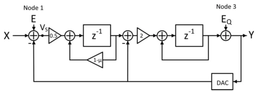
Fig. 3.1: Block diagram of single-loop 2nd-order SDM
Consider the five independent noises. The modified quantization noise (3.4) is expressed in Fig. 3.1 as EQ applied at nodes 3 and the factor μ at feedback loop of first
integrator. The remaining four noises are applied at node 1 of Fig. 3.1, the sum of which is donated as E. These five noises are treated as independent because EQ and the four noises in
E are all assumed to be Gaussian and white. Next, to explain why these five noises are correlated to settling noise, recall that settling error ε is approximated in [18] as
1 3 5 1VS 3VS 5VS
(3.5)
According to Fig. 3.1, the VS in equation (3.5) can be expressed as
-2 1 2
(1- ) -[1 (1 )]
S Q
It is clear from equations (3.5) and (3.6) that settling error ε is correlated to E, EQ and μ.
From discussions above, the noise signal at SDM output can be expressed as
_ _ _
( ) ( ) ( ) ( )
N Modified quantization noise Settling noise E
v t v t v t v t (3.7)
where
_ _ _ _
( ) ( ) ( ) ( ) ( )
E Switch thermal OTA thermal DAC noise Jitter noise
v t v t v t v t v t (3.8)
The autocorrelation function of vN(t) is
_ _ _
( ) [ ( ) ( )]
( ) ( ) ( )
( ) ( ) ( ) ( )
N N N
Modified quantization noise E Settling noise
SQ QS SE ES R E v t v t R R R R R R R (3.9)
where RSQ(τ) and RQS(τ) are cross-collection function of vSettling_noise(t) and
vModified_quantization_noise(t), and RSE(τ) and RES(τ) are cross-collection function of vSettling_noise(t)
and vE(t). Since vModified_quantization_noise(t) and vE(t) are uncorrelated, thus, REQ(τ) and RQE(τ)
do not exist in equation (3.9). Then, the power spectral density function of vN(t) is
_ _ _
( ) { ( )}
( ) ( ) ( )
( ) ( ) ( ) ( )
N N
Modified quantization noise E Settling noise
SQ QS SE ES S f F R S f S f S f S f S f S f S f (3.10)
where SSettling_noise(f), SQuantization_noise(f), and SE(f) represent PSD of vSettling_noise(t),
vModified_quantization_noise(t), and vE(t). The SSQ(f) and SQS(f) are the cross spectral density
between vModified_quantization_noise(t) and vSettling_noise(t). The SSE(f) and SES(f) are the cross
spectral density between vE(t) and vSettling_noise(t). Thus, the in-band noise power PN of
equation (3.1) can be obtained by
_ _ _ _ _ _ _ -( ) ( ) ( ) ( ) ( ) B B B B f N f N
Modified quantization noise Switch thermal OTA thermal DAC noise Jitter noise f Settling noise f SQ QS SE ES P S f df P P P P P P S f S f S f S f df
(3.11)terms at equation (3.11) are the correlation power models to be derived. The SQS(f), SSQ(f),
SSE(f) and SES(f) can be approximated as [21]
* * _ _ _ * * _ ( ) ( ) 1 ( ) ( ) 2 ( ) ( ) 1 ( ) ( ) 2 SQ QS
Settling noise Modified quantization noise
SE ES Settling noise E S f S f V f V f T S f S f V f V f T (3.12)
where VSettling_noise(f), VModified_quantization_noise(f), and VE(f) are the Fourier transforms of
vSettling_noise(t), vModified_quantization_noise(t), and vE(t), respectively, over a finite time interval [-T,
T].
(a)
(b)
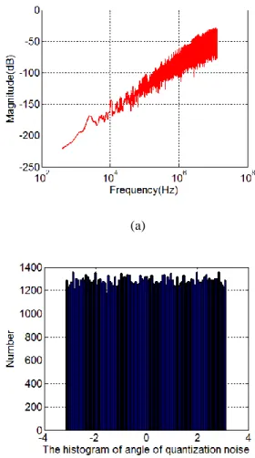
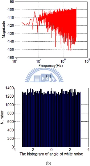
Fig. 3.2: The magnitude and angle of VModified_quantizaition_noise(f)
Fig. 3.2 (a) shows the FFT of a typical vModified_quantization_noise(t) obtained from behavior
close to uniform distribution. Therefore, θQ(f) is assumed to be an arbitrary value in –π~π,
and VModified_quantization_noise(f) is modeled as
_ _ 2 ( ) ( ) 2sin 4 sin 12 Q
Modified quantization noise
i f LSB S S S V f V f f e f f f (3.13)
Fig. 3.3 shows the FFT of vE(t) obtained from behavior simulation.
(a)
(b)
Fig. 3.3: The magnitude and angle of VE(f)
The angle of VE(f) is also close to a uniform distribution. Therefore, θE(f) is assumed to be
an arbitrary value in –π~π, and VE(f) is modeled as
1/ 2 1/ 2 _ _ ( ) 1/ 2 1/ 2 _ _ 1( ) Switch thermal OTA thermal iE f
E
S
Jitter noise DAC noise
P P V f e f P P (3.14)
1 3 5 _ ( ) 1 ( ) 3 ( ) 5 ( ) Settling noise S S S v t v t v t v t (3.15) _ ( ) 1 1( ) 3 3( ) 5 5( ) Settling noise S S S V f V f V f V f (3.16)
where vS(t) is the first integrator input signal, and by equation (3.6)
1 4 / _ _ ( ) ( ) (1 S) ( ) ( ) S S j f f
E Modified quantization noise
V f V f
e V f V f
(3.17)
Then, the Fourier transform of vS2(t) can be obtained by convoluting VS(f) and VS(f), i.e.
2( ) ( ) ( )
S S S
V f V f V f (3.18)
Subsequently, VS3(f) and VS5(f) can be obtained by
3( ) 1( ) 2( ) S S S V f V f V f (3.19) 5( ) 2( ) 3( ) S S S V f V f V f (3.20)
With VQuantization_noise(f), VE(f), and VSettling_noise(f) described in equations (3.13), (3.14) and
(3.16), the cross-spectral densities, SQS(f), SSQ(f), SSE(f) and SES(f), can be computed, and
then the correlation power can be evaluated as
- ( ) ( ) ( ) ( ) B B f Correlation f SQ QS ES SE P
S f S f S f S f df (3.21)With PCorrelation added, PN in equation (3.1) is then rewritten as
_ _ _ _ _ _
_
N Modified quantization noise Switch thermal OTA thermal Jitter noise DAC noise
Settling noise Correlation
P P P P P P
P P
(3.22)
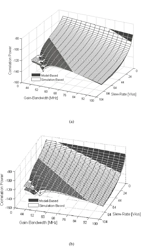
To verify the correctness of correlation model (3.21), Fig. 3.4 (a) (b) shows the correlation power calculated by equation (3.21) and by behavior simulation for various SR and GBW combinations, with other parameters set at Fin=100kHz, B=1, OSR=100,
(a)
(b)
Fig. 3.4: Correlation powers (a) assumption that VE in negligible (b) assumption that VE exists
Next, an example is provided to investigate the relations between PSettling_noise,
PQuantization_noise and PCorrelation under the assumption that VE(f) in negligible, which is the
typical case. The relevant parameters are: Fin=100kHz, B=1, OSR=256, Ain=0.2V, Vref=1V
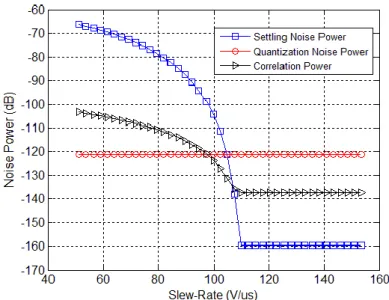
Fig. 3.5: Each noise power for different SR values.
Discussion 1: As Fig. 3.5 shows, settling noise is in linear region [18] when slew-rate is large than 110V/μs. In this case, the α3 and α5 in equation (3.16) can be neglected, such
that
_ ( ) 1 1( )
Settling noise S
V f V f (3.23)
Then, it can be shown that
1/2 _ _ ( ) ( ) 2 B B fCorrelation f SQ QS Quantization noise Settling noise
P S f S f df P P
(3.24)Since PQuantization_noise=-120dB and PSettling_noise=-159dB, the correlation power is -137dB, as
is shown in Fig. 3.5.
Discussion 2: When slew-rate is less than 110 V/μs, the α3 and α5 in equation (3.16)
would increase dramatically. Therefore, the normalized correlation between settling noise and quantization noise reduces when slew-rate decreases. However, as is shown in Fig. 3.5, PCorrelation increases steadily as SR decreases, and PCorrelation becomes larger than
PQuantization_noise when SR<100 V/μs. This is because PCorrelation represents an absolute
4
Advantages of Model-Based SDM Design
The first advantage of model-based design over simulation-based design is obviously its speed; the former can be at the order 104 times faster. The second advantage is that the model-based approach provides more insights to guide the design, since this design method explicitly computes all noise powers and distortion powers. These issues are quantitatively analyzed in this chapter.
4.1 SNDR Speed Comparison
For model-based SDM design, the SNDR is computed by equation (3.1). In simulation-based SDM design (in MATLAB SIMULINK environment), generating SNDR is a more complex process. First, behavior simulation is conducted and output data points are collected. Then, FFT is performed on collected data points to generate power spectral density (PSD). The total noise power PN is obtained from integrating in-band PSD floor, and
total distortion power is obtained by summing up distortional powers in PSD. The accuracy of SNDR computed heavily depends on the number of data points involved, since sufficient number of data points in needed to generate relatively accurate PSD [22]. However, more data points require almost proportionally more simulation time because FFT accounts for only 0.3% of the total simulation time for generating SNDR. Table 4.1 lists the simulation times for obtaining 16384, 32768 and 65536 data points.
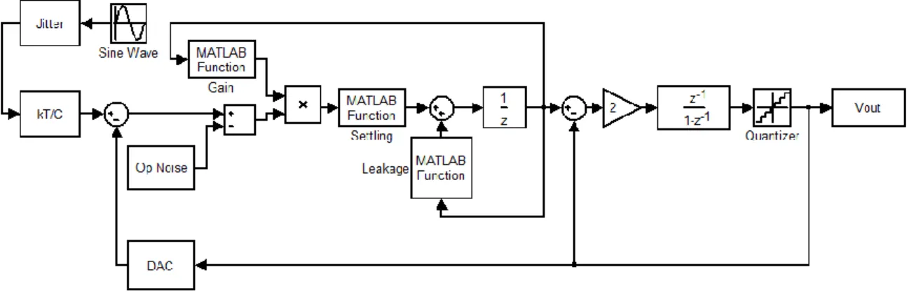
Fig. 4.1: Single-loop 2nd-order SDM model with relevant non-ideality blocks. TABLE 4.1: Running time of each non-ideality for both design approaches
Non-idealities Data Points 16384 32768 65536
Quantization Noise Simulation-Based 56.515ms 114.125ms 285.375ms Model-Based 0.016ms 0.016ms 0.016ms Switch thermal Noise Simulation-Based 108.203ms 182.969ms 423.25ms Model-Based 0.016ms 0.016ms 0.016ms Jitter Noise Simulation-Based 67.985ms 123.703ms 254.562ms Model-Based 0.016ms 0.016ms 0.016ms DAC Noise Simulation-Based 83.86ms 165.157ms 370.297ms Model-Based 0.016ms 0.016ms 0.016ms OTA thermal Noise Simulation-Based 65.438ms 119.219ms 256.844ms Model-Based 0.422ms 0.422ms 0.422ms Settling Noise Simulation-Based 2171.72ms 4865.94ms 8578.59ms Model-Based 23.469ms 23.469ms 23.469ms DC-Gain Distortion Simulation-Based 1967.063ms 3941.09ms 7828.078ms Model-Based 0.031ms 0.031ms 0.031ms Total Non-idealities Simulation-Based 3847.03ms 7631.25ms 15382.03ms Model-Based 24.125ms 24.125ms 24.125ms
In MATLAB 7.0.1, simulations were carried on AMD Athlon (tm) 64 X2 Dual Core Processor 6000+ PC with 4GB memory running at 3.11GHz.
In contrast, as is shown in Table 4.1, in model-based approach the SNDR computation time is a least 102 times loss than that in simulation-based approach. The model-based SNDR computation time can be reduced much further, since little research has been done on
the computational issue which would be discussed in follows.
As Fig. 4.2 shows, computing settling noise power accounts for 97% of the total time for generating SNDR. To reduce the computation time of settling noise power, we modify the settling noise analytic model [18].
Fig. 4.2: The pie chart of SNDR computation time in model-based SDM design method
The settling noise is approximated by following polynomial
1 3 5 _ 1 3 5
Settling noise S S S
v v v v (4.1)
First, coefficients α1, α3 and α5 are computed by
1 2 4 6 0 0 0 1 4 6 8 3 0 0 0 5 6 8 10 0 0 0 2 ( ) ( ) ( ) ( ) ( ) ( ) ( ) ( ) ( ) ( ) ( ) H H H H H H H H H V V V S S S S S S S S S V V V S S S S S S S S S V V V S S S S S S S S S S S S S W V V dV W V V dV W V V dV W V V dV W V V dV W V V dV W V V dV W V V dV W V V dV W V V dV W V
1 1 0 4 1 3 0 6 1 5 0 ( ) ( ) ( ) ( ) L H S L L L H S L L L H S L L V V V V L S S V V V V V S S S V S L S S V V V V S S S V S L S S V e e V dV W V V dV W V V e e V dV W V V dV W V V e e V dV
(4.2)where W(VS) is the weight function,
2 2 0 1 ( ) exp 1 exp 2 2 2 2 H S S s H S V s V V s V V W V V dV
(4.3)3 ( ) ( ) ( ) ( ) S S S S V f V f V f V f (4.4) 5 ( ) ( ) ( ) ( ) ( ) ( ) S S S S S S V f V f V f V f V f V f (4.5)
Finally, the settling noise power is obtained by
1 3 5 _ 1 ( ) 3 ( ) 5 ( ) B B f Settling noise f S S S P V f V f V f df
(4.6)In computing settling noise power, simulation result indicates that the first step, i.e., the coefficient computation, is the most time-consuming because using MATLAB to evaluate integrals in equation (4.2) costs much time. In MATLAB environment, dealing with algebra problem is much faster than evaluating integral problem. Hence, find the antiderivative of integrand in equation (4.2) and substitute the upper and lower limits of integration would make computation time for coefficients α1, α3, and α5 much faster. In this way the
computation time for coefficients α1, α3 and α5 become much faster, and it only takes
0.219ms to generate settling noise power.
In addition, computing OTA thermal noise power also needs to evaluate the integrals in equation (4.7). Hence, we find the antiderivative of integrand in equation (4.7) and substitute the upper and lower limits of the integration to reduce the running time of computing OTA thermal noise power. In this way it takes 0.016m second for generating OTA thermal noise power.
2 2 2 _ 2 0 1 2 2 1 1 2 2 0 2 1 1 1 1 ( ) ( ) 2 1 1 1 10 4 1 2 1 1OTA thermal nOTA Samp Int
S L S S P V H f H f df a OSR a RC a kT d a OSR C A RC a A a RC GBW GBW
(4.7)Eventually, it takes only 0.312m second for generating SNDR in model-based SDM design after modifying noise analytic models. It is hundred times faster than before. But computing
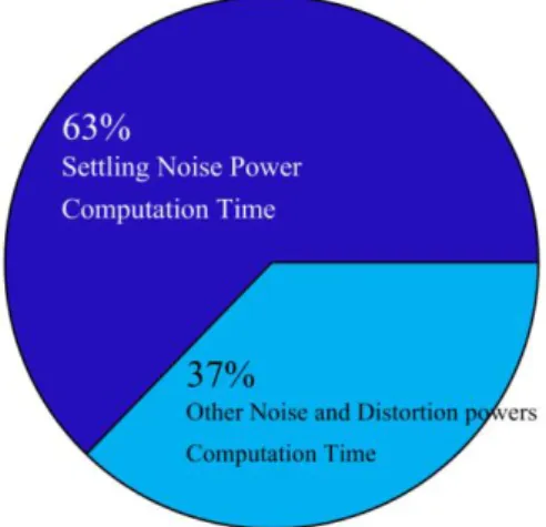
settling noise power still accounts for 63% of the total time in generating SNDR as is shown in Fig. 4.3.
Fig. 4.3: The pie chart of SNDR computation time in modified model-based SDM design method
Despite the detail of two design approaches, in model-based SDM design the SNDR computation time is a least 104 times faster than that in simulation-based SDM design. Consequently, model-based method is a time-efficient and practical solution in SDM design cycle.
4.2 SDM Design Guide
Simulation-based SDM design generates sum of noise PN and sum of distortion PD
from SDM output PSD. In this process, it is not easy to find out the magnitude of individual noise or distortion. In contrast, model-based SDM design can explicitly compute all noise and distortion powers. This advantage may be exploited by designers. We now consider two possible cases.
In the case that design specification cannot be met, the knowledge about dominating noise or distortion would indicate where design can be improved. For example, in a design problem for the sensor applications, SNDR is required to be better than 96dB (i.e., a resolution of 16 bits), but SNDR at 87dB is the highest that is achieved by traditional design method. After computing noise and distortion powers using their models, it revealed that all noises and distortions are very small except that the DAC noise at -86dB is the dominating
factor for previous design result. This gives a guide about how the design can be improved. After employing the DWA algorithm or making use of better CMOS device technology, the designer is able to reduce DAC noise to -123dB. New computations reveal that SNDR at 97dB is achieved, with dominating non-ideality power being switch noise power at -99dB.
In the case that design specification is met, the knowledge about magnitude of each noise or distortion would suggest where design parameters can be relaxed. For example, SNDR for an audio application is required to be better than 84dB (i.e. a resolution of 14 bits), and SNDR at 87dB is achieved by traditional design method. Since our model can compute all noise and distortion powers, we immediately find that -121dB for the settling noise power is by far smaller than the dominating non-ideality power which here is switch thermal noise at -94dB. Our models suggest that adjusting SR and GBW would significantly affect settling noise power and SDM power consumption, but otherwise has little effect on other noises and distortions. After relaxing design parameters SR (from 160V/μs to 91V/μs) and GBW (from 120MHz to 80MHz), designer raised settling noise to -98dB. Although SNDR is consequently lowered to 86dB, it still meets the 84dB requirement. But the benefits received are obvious: OTA power consumption is reduced from 11.23mW to 7.04mW, and OTA design complexity is much decreased.
5
Models of SDM Power Consumption
In this chapter, we propose an effective SDM power consumption model, which bases on single-loop 2nd-order SDM architecture shown in Fig. 2.1. Our power consumption model is split up in two parts: the analog power consumption of OTA and quantizer, and the digital power consumption of switch, DAC and data weighted averaging (DWA).
5.1 Analog Power Consumption:
5.1.1 OTA Power Consumption:
Given design parameters GBW, SR, and Ceq, OTA power consumption is derived partly
based on study [23] [24]. Here, OTA model is depicted in Fig. 5.1. This model includes: A single-pole dynamic
A non-linear characteristic with maximum output current IO
Fig. 5.1: OTA model
The OTA open-loop transfer function can be expressed as
0 1 ( ) 1 A A s s p (5.1)
A0 is the OTA open-loop dc gain
0 m out
A g r (5.2)
where gm is the OTA transconductance and rout is the OTA open-loop output resistance.
1 1 out L p r C (5.3)
where CL donates the open-loop effective load capacitance.
Using OTA model shown in Fig. 5.1 with infinite rout, the model of the SC integrator is
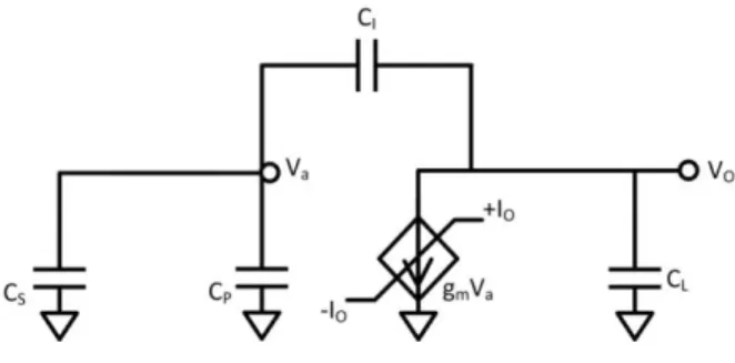
shown in Fig. 5.2. Meanwhile, it also takes the parasitic capacitors associated to its input and output nodes into account.
Fig. 5.2: Integrator model with the parasitic capacitor
Here, CS and CI are the sampling and integrating capacitors of integrator; CP is the parasitic
input capacitance and CL is the output load capacitance, which includes the OTA output
node parasitic and the bottom plate parasitic of CI. For the SC integrator, the close-loop
transfer function is 1 1 ( ) 1 CL u A s s f f (5.4)
where f is the feedback factor of integrator, and ωu is the OTA unity-gain frequency. The
feedback factor for the integrator is
I S I P C f C C C (5.5)
The unit-gain frequency for integrator is
0 1 m u O g A p C (5.6)
where CO is the open-loop effective load capacitance of the integrator shown in Fig. 5.2.
/ /( )
O L I S P
C C C C C (5.7)
3 m dB u eq g f C (5.8)
where Ceq is the equivalent load capacitance for the integrator, and is estimated as
1 P S eq P S L I C C C C C C C (5.9)
For the step response calculation, the time constant τa of the integrator is defined as
3 1 2 m dB a eq g GBW C (5.10)
Then, OTA transconductance for the integrator is obtained by 2
m eq
g GBW C (5.11)
Besides, SR for the integrator is defined as
O eq I SR C (5.12)
Hence, OTA maximum output current IO is obtained by
O eq
I SR C (5.13)
Given specific values of GBW, SR and Ceq, equation (5.11) and equation (5.13) indicate the
corresponding value of gm and IO of the OTA. However, estimating OTA power
consumption is not only determined by these three design parameters, but also decided by chosen OTA topology. The merits of three OTA topologies here are examined: telescopic OTA, folded-cascode OTA, and two-stage Miller-compensated OTA. Their simplified circuit schematics would be presented in Fig. 5.3 (a), (b) and (c), respectively.
Fig. 5.3 (a) Telescopic OTA
For telescopic OTA, the slew-rate is
9 D eq I SR C (5.14)
Then, the bias current ID9 corresponded to SR is defined as
9( )
D SR eq
I SR C (5.15)
The close-loop -3dB bandwidth for the integrator is
1 3 m dB eq g C (5.16)
Combing (5.17) with the transcoductance equation in strong region inversion region,
9 1 1 1 1 2 D D m OV OV I I g V V (5.17)
The bias current ID9 corresponded to ω-3dB is defined as
9( ) 3 1 2 1
D GBW dB eq OV eq OV
I C V GBW C V (5.18)
where VOV1 is the transistor overdrive voltage of the differential pair.
Equation (5.15) and equation (5.18) indicate that the telescopic OTA bias current ID9
depends on VOV1. The designer could assume that VOV1 has a range (such as 0.1v~0.3v)
equation hold.
9( ) 9( )
B D SR D GBW
I I I (5.19)
If VOV1 is out of range, it would be stuck at the extreme value of the range and the following
equation would be hold.
9( ), 9( )
B D SR D GBW
I Max I I (5.20)
Finally, the telescopic OTA power consumption is
DD B
PCV I (5.21)
where VDD donates the supply voltage.
Fig. 5.3 (b): Folded-Cascode OTA
For folded-cascode OTA, the slew-rate is
11 D eq I SR C (5.22)
Then, the bias current ID11 corresponded to SR is defined as
11( )
D SR eq
I SR C (5.23)
Notice that the value of ID9 and ID10 is set to 1.2∙ID11 to avoid zero current in cascades when
OTA is slewing [25], and slew limiting occurs only in the input stage of the circuit. The close-loop -3dB bandwidth for the SC integrator is
1 3 m dB eq g C (5.24)
Combing (5.24) with the transcoductance equation in strong region inversion region, the bias current ID11 corresponded to ω-3dB is defined as
11( ) 3 1 2 1
D GBW dB eq OV eq OV
I C V GBW C V (5.25)
Equation (5.23) and equation (5.25) indicate that the folded-cascode OTA bias current ID11
depends on VOV1. The designer could assume that VOV1 has a range when calculating ID11. If
VOV1 is in the range, it would be self adjusted to make following equation be hold.
11( ) 11( )
B D SR D GBW
I I I (5.26)
If VOV1 is out of range, it would be stuck at the extreme value of the range and the following
equation would be hold.
11( ), 11( )
B D SR D GBW
I Max I I (5.27)
Finally, the folded-cascode OTA power consumption is 2.4 DD B
PC V I (5.28)
Fig. 5.3 (c): Two-stage Miller-compensated OTA
For the two-stage Miller-compensated OTA, the slew-rate is
7 2 9 min D , D min( , ) int ext C O C I I SR SR SR C C C (5.29)
6 2 m O g p C (5.30) The zero is 6 0 m C g z C (5.31)
And the unit-gain bandwidth is
1 m u C g C (5.32)
Assuming that phase margin is greater than 70°, and z0 is twenty times higher than ωu, p2
must be placed at least 3.2 times higher than ωu. From the assumption above, we get CC >
0.16CO, and the internal slew-rate SRint is the limiting factor.
Then, the close-loop gain -3dB bandwidth is
1 3 m dB u eq g f C (5.33)
where Ceq for two-stage Miller-compensated OTA is expressed as
1 S P eq C I C C C C C (5.34)
Combing (5.33) with the transcoductance equation in strong region inversion region, the bias current ID7 corresponded to ω-3dB is defined as
7( ) 3 1 2 1
D GBW dB eq OV eq OV
I C V GBW C V (5.35)
Besides, the bias current ID7 corresponded to SR is defined as
7( )
D SR C
I SR C (5.36)
Equation (5.35) and equation (5.36) indicates that the two-stage Miller-compensated OTA bias current ID7 depends on VOV1. The designer could assume that VOV1 has a range when
calculating ID7. If VOV1 is in the range, it would be self adjusted to make following equation
be hold.
7( ) 7( )
B D SR D GBW
If VOV1 is out of range, it would be stuck at the extreme value of the range and the following
equation would be hold.
7( ), 7( )
B D SR D GBW
I Max I I (5.38)
For ID9 = 20ID1 form assumption above, and IB = 2ID1, the power consumption of two-stage
Miller-compensated OTA is
9
( 2 ) 21
DD B D DD B
PCV I I V I (5.39)
As OTA topology is selected, the total OTA power consumption for SDM is approximated as
OTA SDM
PC K PC (5.40)
where KSDM represent the ratio between the total power consumption of all the OTAs and
OTA in first stage.
5.1.2 Quantizer Power Consumption:
Quantizer in SDM is usually implemented by a flash ADC, and its power consumption is
2B
Quantizer comp Supply
PC I V (5.41)
where Icomp donates the total current of each comparator and must be determined before
computing the quantizer power; VSupply is the comparator supply voltage.
5.2 Digital Power Consumption:
5.2.1 DAC Power Consumption:
For the SC stage structure shown in Fig. 2.1, DAC power consumption is approximated by
2 2
2 2
S S
DAC DAC C u ref S C s ref B
PC N k C V f k C V f OSR (5.42)
where first factor 2 comes from the differential implementation; Cu is the unit feedback
CS in first stage; NDAC is the total number of the unit capacitor in first stage and can be
written as NDAC = 2B.
5.2.2 Switch Power Consumption:
The switch power consumption is approximated by
2
2
Switch Switch Switch Supply B
PC N C V f OSR (5.43)
where NSwitch is the number of total switches in SDM; VSupply is the switch supply voltage;
CSwitch is the switch parasitic capacitance corresponding to the switch structure.
For transmission gate switch circuit, the relation of CSwitch and Ron is estimated as
1 1 2 n p Switch on Supply tn tp L C R V V V (5.44)where L is the channel length of transistors. Given Ron, L and the specific process
technology, CSwitch could be obtained.
5.2.3 DWA Power Consumption:
DWA algorithm used to solve the nonlinearity problem of the feedback DAC can be implemented with an accumulator and a logarithmic shifter [27], as is depicted in Fig. 5.4.
Fig. 5.4: Block diagram of DWA implementation
and logarithmic shifter. A 2-bit ROM encoder is shown in Fig. 5.5.
Fig. 5.5: 2-bit thermometer-to-binary ROM encoder
When NMOS turns on, the current flows through the resistor and can be calculated as equation (5.44).
2 DD DS DS D n ox GS t DS V V W V I C V V V R L (5.45)When the NMOS turns off, there is no current on the resistor and no power consumption. For example, as input thermometer code is 0000, the output binary code is 000, and then the ROM encoder consumes no power. As the input thermometer code is 0001, the output binary code is 001, and the power of the ROM encoder is VDD∙ID (Because one NMOS turns
on). For the input thermometer code is given over some time interval, ROM encoder power consumption can be estimated.
For the accumulator and the logarithmic shifter, their power consumption are approximated as
2 , 2
DWA D eq Supply B
PC C V f OSR (5.46)
where VSupply is the circuit supply voltage; CD,eq is the equivalent capacitance corresponding
to the complexity of the accumulator and the logarithmic shifter, and its derivation is based on study [26]. Here, accumulator builds up with register and adder, and logarithmic shifter builds up with multiplexer. Therefore, a good approximation of CD,eq is the number of one
bit accumulator and logarithmic shifter that are operating at frequency fS, and is expressed
as
, ( ) 2
B
D eq Add Reg MUX
C B C C B C (5.47)
where CAdd, CReg, and CMUX are the one bit equivalent capacitance of adder, register and
multiplexer, respectively.
For example, when we give CD,eq a specific value shown in Table 5.1, Fig. 5.6 (a)-(c) show
the DWA power in equation (5.45) with the corresponding simulation result.
TABLE 5.1: The specific value of CD,eq for different bit number
2 Bit 3 Bit 4 Bit
CD,eq 0.2935 pF 0.4846 pF 0.8295 pF
Fig. 5.6 (a): 2-bit DWA Power
Fig. 5.6 (b): 3-bit DWA Power
Fig. 5.6 (c): 4-bit DWA Power
By summing up all the contributions in equations (5.40) - (5.43) and (5.46), the SDM power consumption can be estimated as
OTA Quantizer DAC Switch DWA
POWERPC PC PC PC PC (5.48)
6
Model-Based SDM Design Optimization
In this chapter, we propose a methodology for model-based SDM design optimization. This design method is applied to a published design task [3]. Compared with the single-loop SDM reported in [3], the SDMs designed by our method achieves much higher SNDR and significantly lowers power consumption. This shows that our method can effectively achieve more balanced designs for piratical application.
6.1 Design Optimization Schemes
A typical SDM design optimization algorithm is shown in Fig. 6.1. This algorithm searches the SDM design parameter space to find out one design parameter set which meet in terms of SNR or SNDR while keeping the power consumption as low as possible. The blocks or signals in Fig. 6.1 are explained in the following.
Fig. 6.1: Design optimization schemes
6.1.1 Design Parameters
Designers need to determine which design parameters are fixed to a specific value and which design parameters are adjusted during the optimization process run.
SNDR computation has been described in equation (3.1), and the POWER computation has been described in equation (5.48).
6.1.3 Cost Function Generation
After the SNDR and POWER are computed, they are used to generate 10 log( ) B POWER COST FUNCTION K SNDR f (6.1)
which is a modified figure of merit (FOM) [22]. The factor K served as the relative weighting. If high resolution design is required, the value of K can be set bigger, and increasing SNDR would play a more important role than reducing POWER. In contrast, if low power design is needed, the value of K would be set smaller.
At the end of the optimization process, the design parameter set corresponding to the minimum cost function value is treated as the design.
6.2 ΣΔ ADC for ADSL-CO Applications
The ADSL design specs reported in [3] to be achieved are
Peak SNDR : 78 dB
Signal bandwidth : 276 kHz
According to [3], Vref and VDD are set at 0.9V and 1.8V for the 0.18-μm CMOS technology.
The σdac is set at 0.04% for the MIM capacitance. Design parameter space searched by our
model-based optimization scheme is
B: 1 ~ 4 OSR: 8~96 CS: 0.1 ~1.7 pF A0: 45 ~ 55 dB GBW: 80 ~ 400 MHz SR: 50 ~ 500 V/μs
R: 100 ~ 300 Ω Ain: 0.1 ~ 0.9 V
The design published in [3] and that achieved from our methodology are listed in Table 6.1. The noise powers and distortion powers for both designs are listed in Table 6.2.
TABLE 6.1: Comparisons of our design results with those in [3]
Design parameters Reference [3] K = 0.2 Unit
B 3 2 - OSR 96 96 - CS 1.7 1.12 pF A0 55 50 dB GBW 400 160 MHz SR 500 201 V/μs Ain 300 300 V SNDR reported in [33] 0.638 0.45 dB SNDR(Our model) 78 - dB SNDR(SIMULINK) 75.51 89.91 dB POWER(Our model) 75.17 87.08 mW
TABLE 6.2: The corresponding noise and distortion power for both designs
Non-ideality Power Reference [3] K = 0.2 Unit
PModified_Quantization_noise -109.69 -103.95 dB PSwitch_thermal -96.92 -95.11 dB POTA_thermal -116.28 -111.97 dB PSettling_noise -216.63 -115.63 dB PDAC_noise -85.68 -123.17 dB PJitter_noise -122.87 -125.90 dB PCorrelation -145.61 -123.36 dB PDC-gain_distortion -95.58 -102.58 dB PDAC_distortion -77.05 - dB
Discussion 1: The design from model-based optimization is better than that of [3], achieving 89.91dB SNDR at 13.22mW compared with 75.51dB SNDR at 34.19mW in [3].
Discussion 2: Ref. [3] chose to use a 3-bit DAC without DWA, resulting in a dominating DAC distortion at -77.05dB and a large DAC noise at -85.68dB which brought
down SNDR. In contrast, our method by nature tries to evenly distribute noise power and distortion power among all noise and distortion categories, while minimizing POWER at the same time. This is the main reason our design can achieve a higher SNDR with lower POWER. Our algorithm selected a 2-bit DAC with DWA, eliminating DAC distortion and lowering DAC noise to -123.17dB.
Discussion 3: The power consumption by SDM of [3] is more than two times that of our SDM. This large power consumption is due to high values of GBW and SR used. Although large GBW and SR values indeed reduce Settling noise to -216dB in [3], this offered no help to boost SNDR.
Discussion 4: The SNDR computed by our model are verified by SIMULINK behavior simuation.
TABLE 6.3:Model-based optimization design results for different K values
Design parameters K = 1 K = 0.2 K = 0.04 Unit
B 3 2 2 - OSR 96 96 64 - CS 1.7 1.1 0.75 pF A0 50 50 50 dB GBW 180 160 80 MHz SR 201 201 100.5 V/μs Ain 0.47 0.45 0.45 V SNDR(Our model) 91.69 89.83 85.47 dB POWER(Our model) 23.11 18.78 8.98 mW
Discussion 5: Table 6.3 shows model-based optimization design results for different K values. It can be observed form Table 6.3 that when K increases, more emphasis is on rising SNDR; when K decreases, more emphasis is on reducing POWER.
7
Conclusions and Future Works
In order to increase the speed of circuit design for sigma-delta ADCs, this thesis offers an efficient optimization method to achieve the most suitable circuit specifications. All the noise and distortion powers also can be obtained after optimization process is performed, and the dominant noise or distortion power can be attenuated by adjusting the design parameters. Our proposed method has acceptable accuracy and fantastic speed, and the flexibility can be enhanced by building more noise or distortion models for different circuit structures.
Further, in order to reduce the time-cost for optimization, the algorithm efficiently search the entire design parameters space to find the design parameter set which satisfies the specifications must to be established.