292 IEEE ELECTRON DEVICE LETTERS, VOL. 28, NO. 4, APRIL 2007
High-Temperature Stable HfLaON p-MOSFETs
With High-Work-Function Ir
3
Si Gate
C. H. Wu, B. F. Hung, Albert Chin, Senior Member, IEEE, S. J. Wang, X. P. Wang, M.-F. Li, Senior Member, IEEE,
C. Zhu, Member, IEEE, F. Y. Yen, Y. T. Hou, Y. Jin, H. J. Tao, S. C. Chen, and M. S. Liang, Fellow, IEEE
Abstract—We report a novel 1000 ◦C stable HfLaON p-MOSFET with Ir3Si gate. Low leakage current of 1.8× 10⁻⁵ A/cm2at 1 V above flat-band voltage, good effective work function of 5.08 eV, and high mobility of 84 cm2/V· s are si-multaneously obtained at 1.6 nm equivalent oxide thickness. This gate-first p-MOSFET process with self-aligned ion implant and 1000◦C rapid thermal annealing is fully compatible to current very large scale integration fabrication lines.
Index Terms—HfLaON, Ir3Si, MOSFET, work function.
I. INTRODUCTION
A
CCORDING to the International Technology Roadmap for Semiconductors, the metal-gate/high-κ is the required technology for the future generation complementary MOSFETs to reduce the undesired large gate leakage current and continue the gate oxide scaling [1]–[11]. Currently, the HfSiON is a promising candidate beyond SiON with merits of high-κ value, low gate leakage current, and similar amorphous structure after 1000◦C rapid thermal annealing (RTA) for self-aligned process. However, the lack of a high-work-function gate for HfSiON p-MOSFETs is the challenge since only Ir (5.27 eV) and Pt (5.65 eV) in the periodic table [8] have the needed work function larger than the target 5.2 eV. The other problem of HfSiON is the relative lower κ of 10–14 that causes lim-ited scaling capability. In this letter, we developed the high-temperature stable Ir3Si/HfLaON p-MOSFET to address theaforementioned issues. The novel HfLaON dielectric can pre-serve the amorphous structure after 1000◦C RTA and is similar to HfSiON but with significantly higher κ value. Using high-work-function Ir3Si gate electrode [8], [9], the p-MOSFETs
show good device integrity of low leakage current of 1.8× 10⁻⁵ A/cm2 at 1 V above flat-band voltage Vfb, high
effec-Manuscript received October 26, 2006. This work was supported in part by the National Science Council of Taiwan, R.O.C., under Grant 94-2215-E-009-062. The review of this letter was arranged by Editor A. Chatterjee.
C. H. Wu and S. J. Wang are with the Institute of Microelectronics and Department of Electrical Engineering, National Cheng Kung University, Tainan 701, Taiwan, R.O.C.
B. F. Hung and A. Chin are with the Department of Electronics Engineer-ing, National Chiao-Tung University, Hsinchu 300, Taiwan, R.O.C. (e-mail: [email protected]).
X. P. Wang, M.-F. Li, and C. Zhu are with the Silicon Nano Device Laboratory, Department of Electrical and Computer Engineering, National University of Singapore, Singapore 117576.
F. Y. Yen, Y. T. Hou, Y. Jin, H. J. Tao, S. C. Chen, and M. S. Liang are with the Taiwan Semiconductor Manufacturing Company Ltd., Hsinchu 300, Taiwan, R.O.C.
Color versions of one or more of the figures in this letter are available online at http://ieeexplore.ieee.org.
Digital Object Identifier 10.1109/LED.2007.892367
tive work function φm-eff of 5.08 eV, high hole mobility of
84 cm2/V· s, and good 1000 ◦C RTA thermal stability at equivalent oxide thickness (EOT) of 1.6 nm. These results are compatible with or better than the best reported metal-gate/high-κ p-MOSFETs [1]–[7].
II. EXPERIMENTALPROCEDURE
Standard N-type Si wafers with resistivity of 1–10 Ω· cm (1015–1016 cm−3 doping level) were used in this study. After standard RCA clean, the HfLaO was deposited on N-type Si wafers by physical vapor deposition and post-deposition annealing. The HfLaON was formed by applying NH3plasma
surface nitridation on HfLaO. Then 5-nm amorphous-Si and 20-nm Ir were subsequently deposited on HfLaON and RTA annealed at 400–1000◦C for 30–5 s to form the MOS capaci-tors. For comparison, Ir/HfSiON devices were also fabricated, where the HfSiON was formed by atomic layer deposition of HfSiO and followed by surface plasma nitridation. The low-temperature-deposited Al gate on 1000◦C RTA-annealed HfLaON capacitors was also formed for φm-eff reference. For
p-MOSFETs, additional thick TaN capping layer is added on Ir/Si/HfLaON to prevent subsequent ion implantation pene-tration, where the IrxSi gate was formed during RTA. Af-ter patAf-terning, self-aligned B+ implantation was applied at
25 keV, and source–drain doping was activated at 1000 ◦C RTA for 5 s. The fabricated p-MOSFETs were character-ized by capacitance–voltage (C–V ) and current–voltage (I–V ) measurements.
III. RESULTS ANDDISCUSSION
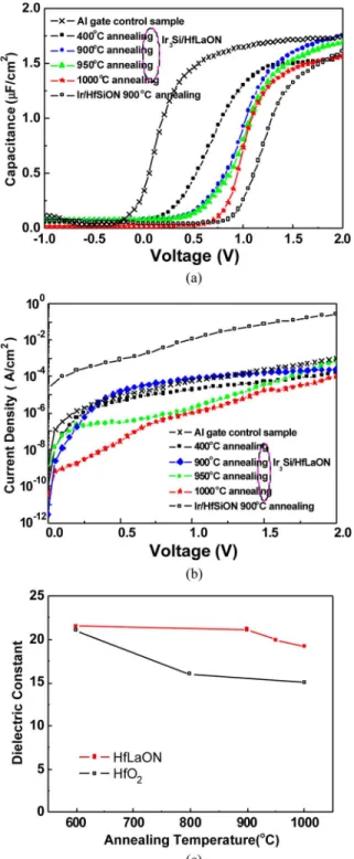
Fig. 1(a) and (b) shows the C–V and J –V character-istics, respectively, for different RTA temperature-annealed IrxSi/HfLaON capacitors. The Ir/HfSiON and Al/1000 ◦ C-annealed HfLaON devices are also shown for comparison. An increasing Vfb trend with increasing RTA temperature is
measured, which is attributed to IrxSi reaction toward high-κ interface [8], [9]. The Ir on HfSiON shows the highest Vfb,
but the capacitor failed after 1000 ◦C RTA. In contrast, the IrxSi/HfLaON has good 1000◦C thermal stability by convert-ing Ir to IrxSi by inserting ∼5 nm amorphous Si; however, the better thermal stability is traded off the slightly lower Vfb.
From the C–V shift to control Al gate on 1000 ◦C RTA-annealed HfLaON, the extracted φm-eff of Ir3Si/HfLaON is
5.08 eV. Here, the Al-gated capacitor was chosen as a refer-ence because low-temperature-deposited pure metal has little 0741-3106/$25.00 © 2007 IEEE
WU et al.: HIGH-TEMPERATURE STABLE HfLaON p-MOSFETs WITH Ir3Si GATE 293
Fig. 1. (a) C–V and (b) J –V characteristics of IrxSi/HfLaON, Ir/HfSiON,
and Al/1000◦C-annealed HfLaON capacitors measured under accumulation. The device area is 100× 100 µm. (c) Dielectric constant of HfLaON and HfO2
at different RTA temperatures.
Fermi-level pinning on high-κ dielectric [4], [5], [8], [9], and the same 1000 ◦C RTA ensures the similar oxide charge in HfLaON to Ir3Si-gated devices. The Al control gate is used
to avoid oxide charge difference on thickness introduced by nitrogen-plasma treatment and process variation. Nonetheless, the fixed charge density should be small from the good mobility shown as follows. The merit of using HfLaON rather than HfSiON is clearly seen by the orders of magnitude leakage
Fig. 2. XRD profiles of the Ir3Si/HfLaON structure.
Fig. 3. Id–Vdcharacteristics of Ir3Si/HfLaON p-MOSFETs. The gate length
is 4 µm.
current improvement. Very low leakage current of 1.8× 10⁻⁵ A/cm2 at 1 V above Vfb is measured in IrxSi/HfLaON at 1.6 nm EOT. Such low leakage current is attributed to the high-κ value of 20 and amorphous structure after 1000 ◦C RTA from cross-sectional transmission electron microscopy measurement. The decreasing stretch of C–V curves with increasing RTA temperature suggests the improving oxide quality, annealing out the defects at high temperatures. There-fore, high φm-eff of 5.08 eV, low gate leakage current of 1.8×
10−5A/cm2(Vfb+ 1 V), and good thermal stability of 1000◦C
RTA can be achieved at the same time in IrxSi/HfLaON MOS capacitors at 1.6 nm EOT. The decreasing capacitance density with increasing RTA temperature is related to slight decreasing κ value reduction shown in Fig. 1(c), but the amount of reduc-tion is significantly less than HfO2.
We have further used the X-ray diffraction (XRD) measure-ments to characterize the IrxSi. As shown in Fig. 2, the Ir-rich IrxSi with x = 3 was formed with distinct 2θ angle to residual Ir peak. The x = 3 in IrxSi was determined by comparing the measured peak XRD pattern with published data [12]. The amorphous structure of HfLaON was also confirmed by glazing angle XRD measurements even after 1000◦C RTA.
Fig. 3 shows the transistor Id–Vd characteristics as a function of Vg–Vt for 1000 ◦C RTA-annealed Ir3Si/HfLaON
294 IEEE ELECTRON DEVICE LETTERS, VOL. 28, NO. 4, APRIL 2007
Fig. 4. Hole mobility as a function of gate electric field of Ir3Si/HfLaON
p-MOSFETs.
p-MOSFETs, and good transistor characteristics are obtained. Here, the Vt is −0.1 V as obtained from the linear Id–Vg plot and consistent with the large φm-eff of 5.08 eV from
C–V curves.
Fig. 4 shows the hole mobility plot as a function of gate electric field of Ir3Si/HfLaON p-MOSFETs. High hole
mo-bility of 84 and 63 cm2/V· s are obtained at peak value and
1 MV/cm effective field for Ir3Si/HfLaON p-MOSFETs,
re-spectively. This result is comparable with the reported HfSiON p-MOSFET in the literature [1]–[7] with advantages of process compatibility to current VLSI line.
IV. CONCLUSION
Good device integrity of Ir3Si/HfLaON p-MOSFETs is
shown by the very low leakage current, high φm-eff, good
hole mobility, and 1000 ◦C thermal stability. This gate-first self-aligned process is fully comparable to current VLSI fab-rication lines.
ACKNOWLEDGMENT
The authors would like to thank R. N. Kwo, M. H. Hong, and H. L. Hwang of the National Tsing Hua University for their support.
REFERENCES
[1] H.-H. Tseng, C. C. Capasso, J. K. Schaeffer, E. A. Hebert, P. J. Tobin, D. C. Gilmer, D. Triyoso, M. E. Ramón, S. Kalpat, E. Luckowski, W. J. Taylor, Y. Jeon, O. Adetutu, R. I. Hegde, R. Noble, M. Jahanbani, C. El Chemali, and B. E. White, “Improved short channel device characteristics with stress relieved pre-oxide (SRPO) and a novel tantalum carbon alloy metal gate/HfO2stack,” in IEDM Tech. Dig., 2004,
pp. 821–824.
[2] X. Yu, M. Yu, and C. Zhu, “Advanced HfTaON/SiO2gate stack with high
mobility and low leakage current for low-standby-power application,” IEEE Electron Device Lett., vol. 27, no. 6, pp. 498–501, Jun. 2006. [3] S. C. Song, Z. Zhang, C. Huffman, J. H. Sim, S. H. Bae, P. D. Kirsch,
P. Majhi, R. Choi, N. Moumen, and B. H. Lee, “Highly manufacturable advanced gate-stack technology for sub-45-nm self-aligned gate-first CMOSFETs,” IEEE Trans. Electron Devices, vol. 53, no. 5, pp. 979–989, May 2006.
[4] T. Nabatame, M. Kadoshima, K. Iwamoto, N. Mise, S. Migita, M. Ohno, H. Ota, N. Yasuda, A. Ogawa, K. Tominaga, H. Satake, and A. Toriumi, “Partial silicides technology for tunable work function elec-trodes on high-k gate dielectrics-Fermi level pinning controlled PtSixfor
HfOx(N) pMOSFET,” in IEDM Tech. Dig., 2004, pp. 83–86.
[5] K. Takahashi, K. Manabe, T. Ikarashi, N. Ikarashi, T. Hase, T. Yoshihara, H. Watanabe, T. Tatsumi, and Y. Mochizuki, “Dual work function Ni-silicide/HfSiON gate stacks by phase-controlled full-silicidation (PC-FUSI) technique for 45-nm-node LSTP and LOP de-vices,” in IEDM Tech. Dig., 2004, pp. 91–94.
[6] P. F. Hsu, Y. T. Hou, F. Y. Yen, V. S. Chang, P. S. Lim, C. L. Hung, L. G. Yao, J. C. Jiang, H. J. Lin, J. M. Chiou, K. M. Yin, J. J. Lee, R. L. Hwang, Y. Jin, S. M. Chang, H. J. Tao, S. C. Chen, M. S. Liang, and T. P. Ma, “Advanced dual metal gate MOSFETs with high-k dielectric for CMOS application,” in VLSI Symp. Tech. Dig., 2006, pp. 14–15.
[7] H. Y. Yu, R. Singanamalla, K. Opsomer, E. Augendre, E. Simoen, J. A. Kittl, S. Kubicek, S. Severi, X. P. Shi, S. Brus, C. Zhao, J. F. de Marneffe, S. Locorotondo, D. Shamiryan, M. Van Dal, A. Veloso, A. Lauwers, M. Niwa, K. Maex, K. D. Meyer, P. Absi, M. Jurczak, and S. Biesemans, “Demonstration of Ni fully germanosilicide as a pFET gate electrode candidate on HfSiON,” in IEDM Tech. Dig., 2005, pp. 653–656. [8] D. S. Yu, A. Chin, C. H. Wu, M.-F. Li, C. Zhu, S. J. Wang, W. J. Yoo,
B. F. Hung, and S. P. McAlister, “Lanthanide and Ir-based dual metal-gate/HfAlON CMOS with large work-function difference,” in IEDM Tech. Dig., 2005, pp. 649–652.
[9] C. H. Wu, D. S. Yu, A. Chin, S. J. Wang, M.-F. Li, C. Zhu, B. F. Hung, and S. P. McAlister, “High work function IrxSi gates on HfAlON
p-MOSFETs,” IEEE Electron Device Lett., vol. 27, no. 2, pp. 90–92, Feb. 2006.
[10] C. H. Wu, B. F. Hung, A. Chin, S. J. Wang, F. Y. Yen, Y. T. Hou, Y. Jin, H. J. Tao, S. C. Chen, and M. S. Liang, “HfAlON n-MOSFETs incorpo-rating low work function gate using ytterbium-silicide,” IEEE Electron Device Lett., vol. 27, no. 6, pp. 454–456, Jun. 2006.
[11] X. P. Wang, C. Shen, M.-F. Li, H. Y. Yu, Y. Sun, Y. P. Feng, A. Lim, H. W. Sik, A. Chin, Y. C. Yeo, P. Lo, and D. L. Kwong, “Dual metal gates with band-edge work functions on novel HfLaO high-κ gate dielectric,” in VLSI Symp. Tech. Dig., 2006, pp. 12–13.
[12] S. Bhan and K. Schubert, “Constitution of the systems cobalt–germanium, rhodium–silicon, and some related alloys,” Int. J. Mater. Res. (Zeitschrift fuer Metallkunde), vol. 51, pp. 327–339, 1960.