IEEE ELECTRON DEVICE LETTERS, VOL. 12, NO. 11. NOVEMBER 1991 623
Direct Evidence
of
Gate Oxide Thickness
Increase in Tungsten Polycide Processes
S.
L. Hsu, L. M.
Liu,M.
S. Lin, Member, IEEE, andC. Y.
Chang, Fellow, IEEEAbstract-The increase of the "effective" gate oxide thick- ness for W-polycide processes is studied. The samples with as-deposited and annealed W polycide are analyzed by sec- ondary ion mass spectrometry, transmission electron mi- croscopy (TEM), and high-frequency C V measurements. The TEM cross section shows that the gate oxide thicknesses are -244 and -285
hi
for as-deposited and 1000°C annealed samples, respectively. The TEM results agree with that from CY measurements. The TEM analyses provide a direct physical evidence of an additional oxide thickness (-
41hi)
during the W-polycide annealing.I. INTRODUCTION
ECENTLY, more IC manufacturers choose to use tung-
R
sten (W) polycide gates instead of Ti-salicide processes in their CMOS technologies, even down to submicrometer regimes, due to the manufacturability of W-polycide gates. However, in the chemical-vapor-deposited tungsten polycide processes, there are two major concerns. One is the peeling problem [ 11, and the other is the current-drive degradation of MOS devices due to gate oxide thickening during the W-poly- cide processes [2]-[4]. It has been reported that the "effec- tive" gate oxide thickness becomes thicker based on the CV measurement [4]. Wright and Saraswat [2] used an ion implanter to introduce fluorine into the gate oxide, and from the CV measurement and ellipsometer data they concluded that the "effective" oxide thickness increased by the addi- tional oxide thickness rather than the change of the oxide dielectric constant. In this paper, we use transmission elec- tron microscopy (TEM), instead of ellipsometer measure- ments, to directly prove that the gate oxide is indeed physi- cally becoming thicker. To our best knowledge, this direct evidence has not yet been reported elsewhere.II. EXPERIMENTAL
A 250-8, gate oxide was grown at 920°C in a dry 0, ambient. The gate was formed by a 2500-8, POC1,-doped polysilicon and a 2500-8, WSix film. The tungsten silicide was deposited using the GENUS 8710 system. After the polycide pattern was defined, the polycide films were an- nealed at 800, 920, and lOOO"C, respectively, all in 0, /N2 ambients. The ambient was initially filled with 0, at a flow
Manuscript received June 19, 1991; revised August 26, 1991.
S. L. Hsu, L. M. Liu, and M. S. Lin are with Taiwan Semiconductor Manufacturing Company, Hsin-Chu, Taiwan, Republic of China.
C. Y. Chang is with the Department of Electronic Engineering, National Chiao-Tung University, Hsin-Chu, Taiwan, Republic of China.
IEEE Log Number 9104127.
rate of 14 l/min for 20 min, followed by N, with a flow rate also at 14 l/min for 10 min. Instead of furnace annealing, some wafers were annealed by rapid thermal annealing (RTA) at 1100°C in 0, ambient with a flow rate at 2 l/min for 20 s.
The as-deposited and annealed samples were then analyzed by secondary ion mass spectrometry (SIMS), high-resolution transmission electron microscopy, and high-frequency CV measurements. SIMS was used to measure the amount of fluorine diffused into oxides. The TEM cross sections were observed at the (110) pole under multibeam bright-field diffraction conditions for accurate delineation of the morphol- ogy of various polysilicon/oxide/substrate interfaces.
III.
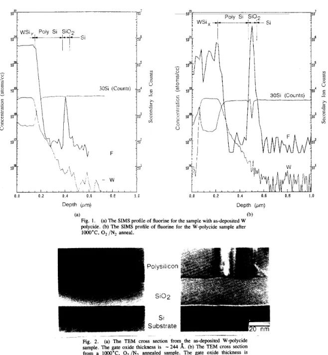
RESULTS AND DISCUSSIONFig. l(a) and (b) shows the SIMS profile of fluorine in W polycide before and after 1OOO"C annealing, respectively. Very high concentration of fluorine is found in gate oxides for the sample annealed at 1OOO"C (see Fig. l e ) ) . The concentration of fluorine is approximately
-
3 x atom/cm3, compared to 5 x 10l8 for the as-deposited sam- ple. The TEM cross section (Fig. 2(a)) from the as-deposited W-polycide sample shows that the gate oxide thickness is-
2448,
and that the polysilicon/gate oxide interface is quite smooth. Fig. 2(b) shows the TEM cross section for the 1OOO"C annealed sample. The gate oxide thickness is-
2858,
and the polysilicon/gate oxide interface is much rougher when compared to that in Fig. 2(a). Comparison between Fig. 2(a) and (b) provides direct physical evidence of an additional oxide thickness (- 41A)
during the W-polycide annealing.The results from CV measurements and TEM analyses for samples annealed at different temperatures are summarized in Table I. The table shows that the oxide thicknesses are the same for the polysilicon gate sample annealed at 1OOO"C and for the as-deposited and after 800°C annealed W-polycide samples. The "effective" gate oxide thickness for W-poly- cide samples is increased as the annealing temperature is above 920°C. Additional oxide thickness increases of 6% and 12% are found for samples annealed at 920 and lOOO"C, respectively. For RTA annealing at 1100°C for 20 s, a 5.2% thickness increase was found. The RTA 1100°C annealing reduces the amount of fluorine diffusion into oxides, and the increased oxide thickness is equivalent to that of the 920°C furnace annealing. The additional oxide thickness obtained from CV measurements agrees with that from TEM analyses.
From the above arguments, we conclude that the increased
624 IEEE ELECTRON DEVICE LETTERS, VOL. 12, NO. 11, NOVEMBER 1991
Process Conditions Poly gate.
+
1OOO"C anneal in 0, /N2WSi, polycide
+
no annealWSi, polycide
+
800°C anneal in 0, /N2WSi, polycide
+
920°C anneal in 0, /N2 WSi, polycide+
1OOO'C anneal in 0, /N2WSi, polycide
+
RTA 1 100"C, O , , 20 s__
1 0 7
t
reductant that can break the Si-0 bonds and displace oxygen at these sites. The released oxygen then diffises to the interfaces, oxidizes silicon and polysilicon, and results in the
IV. SUMMARY
We have shown that fluorine diffised from tungsten sili- tide films to gate oxides causes additional oxide growth. To,
(A)
To,(A)
(from CV) (fromTEM)
-
250
241 244 additional oxide thickness.
250
-
265 - 280 285 263 - (Counts) F C-
Depth O m ) Depth (,urn)
(a) (b)
Fig. 1. (a) The SIMS profile of fluorine for the sample with as-deposited W polycide. (b) The SIMS profile of fluorine for the W-polycide sample after 1000°C, 0, /N2 anneal.
~ _ _ ~~
-Fig. 2. (a) The TEM cross section from the as-deposited W-polycide sample. The gate oxide thickness is
-
244A.
(b) The TEM cross section from a lOOO'C, O,/N, annealed sample. The gate oxide thickness isHSU et a l . : GATE OXIDE THICKNESS INCREASE IN TUNGSTEN POLYCIDE PROCESSES 625
From
CV
measurements, TEM analyses, and SIMS results, we have directly shown that the increased “effective” oxide thickness is actually due to the oxide growth during W-poly- cide annealing.111
P I
131
ACKNOWLEDGMENT
The authors would like to acknowledge help in wafer fabrication from S. L. Ying, C. H. Fang, M. H. Liaw, J. J.
Lin, and Dr. L. S. Tsai. [41
REFERENCES
C. S . Yoo, T. H. Lin, and N. S . Tsai, “Si/W changes and film F l i n g during polycide annealing,” Japan. J . Appl. Phys., vol.
J. Wright and K. C. Saraswat, “The effect of fluorine in silicon dioxide gate dielectrics,” IEEE Trans. Electron Devices, vol. 36,
Y. Shioya, S . Kawamura, I. Kobayashi, M. Madeda, and K. Yanagida, “Effect of fluorine in chemical-vapor-deposited tungsten silicide film on electrical breakdown of SiO, film,” J . Appl. Phys., vol. 61, pp.
R. A. Chapman et al., “0.5 micron CMOS for high performance at 3.3 V,” in IEDM Tech. Dig., 1988, pp. 52-55.
29, pp. 2535-2540, 1990.
pp. 879-889, 1989.