行政院國家科學委員會補助專題研究計畫
■ 成 果 報 告
□期中進度報告
金屬閘極金氧半場效電晶體關鍵技術
Key Technologies of Metal Gate MOSFET
計畫類別:■ 個別型計畫 □ 整合型計畫
計畫編號:NSC 92-2215-E-009-001-
執行期間: 90 年 08 月 01 日至 93 年 07 月 30 日
計畫主持人:崔秉鉞
共同主持人:無
計畫參與人員:黃誌鋒、張修維、梁建翔、吳旻達、呂智勛、蕭逸璿、
王淯正、金立峰、黃勻珮
成果報告類型(依經費核定清單規定繳交):□精簡報告 ■完整報告
本成果報告包括以下應繳交之附件:
□赴國外出差或研習心得報告一份
□赴大陸地區出差或研習心得報告一份
□出席國際學術會議心得報告及發表之論文各一份
□國際合作研究計畫國外研究報告書一份
處理方式:除產學合作研究計畫、提升產業技術及人才培育研究計畫、
列管計畫及下列情形者外,得立即公開查詢
□涉及專利或其他智慧財產權,□一年□二年後可公開查詢
摘
要
本報告包含本三年期計畫之全部成果。內容分為三個部分:金屬閘極技術、高介電 常數介電層技術、製程整合技術。 金屬閘極部分,本計畫提出以具有高、低功函數之金屬形成合金,藉由元素比例調 變功函數的技術,以 Ta-Pt 以及 Ti-Pt 為實例,功函數調變幅度可達 1 電子伏特以上,符 合種金氧半場效電晶體的需求。合金閘極的熱穩定性可達約 900°C,離子植入對功函數 影響極微,製程穩定性極佳。金屬氮化物閘極方面,稍早的計畫已探討過 TaN 閘極,本 計畫則研究 MoN 以及 WN 閘極的性質。藉由反應性離子濺鍍的氮氣流量可以調變金屬 氮化物中的氮含量,功函數會隨之改變,但是調變幅度僅有約 0.4 電子伏特。MoN 的熱 穩定很好,氮含量較高的 WN 在高溫下,會發生氮氣逸出(out-gassing)問題,造成薄膜 剝離。WN 在 HfO2上會有費米能階固定(Fermi-pinning)的問題,MoN 則無此現象。顯見 MoN 是較佳的金屬氮化物閘極材料。 高介電常數介電層技術方面,著重在 HfO2的性質。以物理氣相沈積方式沈積 HfO2 會因為氧氣電漿與矽基板反應生成近似 SiO2 的介面層,使得電容等效二氧化矽厚度偏 厚(CET),即使使用表面氮化處理,仍然效果不佳,恐將無法實用。MOCVD 可以形成 良好的 HfO2薄膜,本計畫改變表面處理方式、氣體導入順序、氣體組成比例、沈積溫 度等製程參數,確定高溫(500°C)、高氧流量(500 sccm)條件下沈積的薄膜性質最佳。此 條件沈積之薄膜經高溫退火,等效氧化層厚度增加極微,漏電流亦不至因結晶化而增 加。穿透式電子顯微鏡分析顯示,退火後局部結晶會造成漏電流增加,但是全面結晶為 緊密的複晶型態則不會有漏電流問題。 製程整合技術方面,首先探討高介電常數介電層的邊緣電場導致能障降低(FIBL) 效應對奈米尺度元件之影響。藉由模擬,確認邊緣電場來自於閘極與汲極重疊處,降低 重疊量可以有效改善此一問題。結合低閘極與汲極重疊、介面層、導電性側壁子等技術, 可將此效應造成的漏電流增加幅度降低到兩倍以下。SOI 結構有較佳的免疫力,因此在 45 奈米世代以下,FIBL 效應不至於構成威脅。Hf 在 SiO2以及 Si 中擴散速率不高,也 不是以離子狀態存在,對於元件隔離以及 pn 接面漏電幾乎不造成影響,不是嚴重的污本計畫三年內有兩名博士研究生、六名碩士研究生、四名大學生參與計畫執行。六 名碩士研究生中的五名已經陸續獲得碩士學位。計畫成果已發表三篇 SCI 期刊論文、六 篇研討會論文,另有三篇期刊論文在審查中。近期的成果將會陸續撰寫成至少三篇期刊 論文發表。專利部分提出九件專利申請,其中兩件已經獲證,另七件在審查中。 關鍵字:金屬閘極、高介電常數介電層、功函數、合金閘極、金屬氮化物、二氧化鉿、 費米能階固定、邊緣電場導致能障降低、金屬污染、濕蝕刻。
Abstract
This final report includes all of the results of the 3-year project. This report is divided into three parts : metal gate technology, high dielectric (high-k) constant dielectric technology, and process integration issues.
In the part of metal gate technology, the novel method of work function modulation was proposed at first. With a proper composition of high and low work function metals, the work function of the metal alloys can be modulated from 4.16eV to 5.05eV continuously. The alloys show good thermal stability and inner chemical activity on both silicon dioxide and hafnium dioxide up to 900°C. The work function does not change after the incorporation of impurities of arsenic ions, boron ions and phosphorus ions. Therefore, the control of threshold voltage of the alloy-gate MOSFET could be easier, and not be disturbed by the S/D implantation process. Metal nitrides are possible metal gate candidates. MoN and WN were investigated in this project. 4. The work function of both metal nitrides increase with the increase of the nitrogen flow rate. The modulation range of work function can be up to 0.4eV from pure metal to metal nitride. 3. Nitrogen within WNx would separate out quickly during rapid thermal annealing and caused the film to crack. MoNx films do not exhibit Fermi-level pinning on both SiO2 and HfO2 while Fermi-level pinning of WNx on HfO2 was observed. Therefore, MoN is a better choice if metal nitride should be used as metal gate.
IN the part of high-k dielectric, we focused on the HfO2 film. It is observed that using physical vapor deposition technique, it is difficult to totally eliminate the formation of interfacial SiO2 layer. During reactive sputtering deposition of HfO2 layer, an interfacial SiO2 layer thicker than 3 nm would be grown. Such an unusual thick SiO2 layer is formed due to the enhanced oxidation of O-radicals generated in the sputtering chamber. The traced oxygen in the sputtering chamber plays critical role on the formation of interfacial layer. The reactive sputtering is not a good method to prepare HfO2 layer with negligible interfacial SiO2 layer. For MOCVD, higher deposition temperature and purer O2 ambient is benefit to the leakage current performance under the same capacitance-equivalent-thickness (CET). Higher O2 flow rate supply more sufficient O2 in reaction chamber is also important deposit high quality HfO2. As the deposition temperature increases to 500℃, the surface treatment and post deposition annealing temperature play minor role on the leakage current. According to the above results,
low temperature or with insufficient O2 supply, the nano-crystals are separated by amorphous region and show round shape. The boundary layer accounts for the leakage current of these samples. Hf-precursor decomposes completely during high temperature deposition, and therefore, with sufficient O2 supply, the film becomes polycrystalline completely. The lack of crystal-amorphous boundary layer results in very low leakage current.
In the part of integration technology, Fringing-Filed-Induced Barrier Lowering (FIBL) effect, Hf contamination, and HfO2 wet etching were studied. TCAD tools were used to investigate the FIBL effect of 25 nm devices. The key factor to affect the FIBL effect is the gate to drain overlap length. Most of the fringing field originates from this region. It is known that stack gate dielectric scheme with buffer layer (k<15) between high-k dielectric and Si substrate can relax the FIBL effect. Conductive spacer is another effective method to reduce the FIBL effect but the process is more complicated. A fully depleted SOI device shows better resistance to FIBL induced Ioff degradation. Therefore, it is concluded that although FIBL effect can not be eliminated, its impact on device performance is diminished at sub-45nm technology node and beyond with suitable device structure. Hf element been knocked into source/drain or field oxide during ion implantation for source/drain extension may be a concern in device fabrication. Fortunately, since the diffusivity of hafnium is very low in both Si and SiO2, we could not observe the effect of hafnium contamination. Our study implies that from the contamination point of view, the HfO2 out of gate electrode have not to be removed immediately after gate patterning. In this project, we also developed a HF+IPA mixture which can etch HfO2 film with reasonable etching rate and acceptable etching rate selectivity with respect to SiO2. These results greatly relax the constraint on device process integration.
In the past three years, 2 Ph.D students, 6 graduate students, and 4 under-graduate students involved this project. Among them, 5 of the 6 graduate students have received their MS degree. Parts of the results have been published as 3 SCI journal papers and 6 conference papers. Another three SCI journal papers are under reviewing procedure. Recent results will be written as 3 SCI journal papers at least. We also applied 9 patents. Two of them have been authorized and the other seven are pending.
Key Words : Metal gate, high dielectric constant dielectric, work function, alloy gate, metal nitride, Fermi-level pinning, hafnium oxide, fringing-field-induced barrier lowering (FIBL), metal contamination, wet etch
Contents
Abstract – Chinese … … … I
Abstract – English … … … .… .III
Contents … … … ..V
Chapter 1. Introduction … … … .1
Part-I
Metal Gate Technology
Chapter 2. Alloy Gate Technology … … … 6
Chapter 3. Process Stability of Alloy Gate … … … ..17
Chapter 4. Metal Nitride Gate Technology – MoN … … … .32
Chapter 5. Metal Nitride Gate Technology – WN … … … ..54
Part-II
High Dielectric Constant Material Technology
Chapter 6. Formation of Interfacial Layer during Reactive Sputtering of
Hafnium Oxide … … … ...77
Chapter 7. Electrical Characteristics of HfO
2Film Prepared by MOCVD ...97
Chapter 8. Physical Characteristics of HfO
2Film Prepared by MOCVD … .134
Part-III Process Integration Issues
Chapter 9. Fringing-Induced Barrier Lowering (FIBL) of Nano-Scale
MOSFETs … … … .165
Chapter 10. A Study on Hafnium Contamination … … … 190
Chapter 11. Wet Etching of HfO
2Film … … … 212
Chapter 1
Introduction
1-1 Project Background
As conventional CMOS devices are scaled down to improve performance, gate engineering becomes a crucial issue. It was found that the conventional gate material, poly-silicon, suffered from gate depletion, high gate resistance, and boron penetration into the channel region in sub-100 nm CMOS technology node [1-5]. Poly-Si gate depletion increases the equivalent gate dielectric thickness by about 3 Å and degrades channel current drive capability [1-3]. High gate resistance increases the RC time delay to degrade high frequency performance. Salicide technology can reduce the gate resistance but it is difficult to maintain a proper aspect ratio for gate stack in scaled devices [4]. Boron penetration in PMOSFET reduces the ability of threshold voltage control and gate oxide reliability [1,5]. High dielectric constant (high k) materials are expected to replace SiO2 for scaling gate dielectric thickness below 1.5 nm where direct tunneling current through SiO2 may be too high to be acceptable [4]. Unfortunately, poly-Si is incompatible with most high k materials due to chemical reaction or interface layer formation [6,7]. It has been demonstrated that metal gate devices are free from gate depletion, high resistance, and boron penetration. Therefore, there is an immense interest in metals to be a replacement of gate electrode.
As the gate oxide thickness of metal–oxide–semiconductor (MOS) devices is scaled down to below sub-1.5nm tunneling current through gate dielectrics and reliability would become serious problems. Therefore, high dielectric constant (high-k) materials, such as ZrO2-based [8] HfO2-based [9] and Al2O3-based [10] metal oxide insulators, have been received considerable attention as alternative dielectric materials. They have been demonstrated to suppress the leakage current significantly as compared to the traditional SiO2-based dielectrics with the same equivalent oxide thickness (EOT) because of their thicker physical thickness. Among these candidates, HfO2 and its silicate not only have relatively high dielectric constants and wide band gaps, but also have been shown impressively thermal stability in contact with silicon substrate [11]. Therefore, HfO2-based
challenging issues, such as formation of interfacial layer and mobility degradation in MOSFET devices, have to be further investigated.
Even if suitable high-k dielectric technology can be developed successfully, a side effect called fringing-induced barrier lowering (FIBL) arising from the use of high-k gate dielectric has been reported [15-20]. The fringing electric field originated at drain penetrates into channel through the high-k gate dielectric and suppress the barrier height from source to channel. Therefore, the off-state drain current (Ioff) increases and the maximum allowable k value of high-k dielectric is limited by the FIBL effect. Some works discussed the effect of device structure on FIBL. Yeap et al reported that remaining high-k dielectric under spacer greatly enhances the FIBL [15]. It is also proposed that an oxide buffer layer under high-k dielectric can suppress the FIBL. Therefore, the impact of high-k dielectric on device structure selection at sub-65nm technology node must be examined.
Most high-k materials, including HfO2, belong to metal oxides, and metal contamination issue must be considered carefully. Metal contamination may come from equipment itself. It had been published that wafer surface becomes rough after standard RCA clean in hafnium-contaminated solution so that gate oxide integrity is degraded [21]. No literature studies metal contamination issues from the metal oxide on device. The self-contamination is very important to determine the device integration scheme.
High-k material is difficult to be etched by either dry etch or wet etch especially for thin film after high temperature annealing [22]. It is hard to remove HfO2 film after gate electrode etching because dry etching of HfO2 may damage the S/D extension region and wet etching of HfO2 exhibit very poor selectivity between high-k dielectric and field oxide. Novel method must be developed to remove HfO2 with low damage and high selectivity to the pre-existed material before integrating HfO2 into MOSFETs.
According to the numerous issues mentioned above, we proposed a three-years project entitled “Key Technologies of Metal Gate MOSFET“ to try to solve these issues. This is the final report of this project.
modulation. In chapter-3, the thermal and process stability of the proposed alloy gate were examined. In chapter-4 and chapter-5, metal nitrides of MoN and WN as gate electrode were examined, respectively.
Chapter-6 discusses the electrical properties and the interfacial layer formation of HfO2 film prepared by PVD method. The electrical characteristics of HfO2 film prepared by MOCVD are presented in chapter-7. The physical analyses of the MOCVD HfO2 film are discussed in chapter-8.
The FIBL effect of nano-scale MOSFET with channel length down to 25 nm was studied using TCAD tools and the results are shown in Chapter-9. Hf contamination due to the incorporation of HfO2 into front-end process of line is studied in chapter-10. We also developed novel chemistry to remove HfO2 film with low damage and high selectivity to SiO2. The results are presented in chapter-11.
Chapter-12 summaries the important conclusion achieved in this three years. The publications and patents generated from the execution of this project are listed in the appendix.
References
[1]. B. Yu, D. H. Ju, N. Kepler, T. J. King, and C. Hu, in Proceedings of the IEEE Symposium on VLSI Technology, p.105(1997).
[2]. K. Chen, M. Chan, P. K. Ko, C. Hu, and J. H. Huang, Solid-State Electron, 38, 1975 (1995).
[3]. N. D. Arora, R. Rios, and C. L. Huang, IEEE Trans. Electron Devices, ED-42, 935(1995).
[4]. The International Technology Roadmap for Semiconductors, p.123, Semiconductor Industry Association, San Jose, CA (1999).
[5]. J. R. Pfiester, F. K. Baker, T. C. Mele, H. H. Tseng, P. J. Tobin J. D. Hayden, J. W. Miller, C. D. Gunderson, and L. C. Parrillo, IEEE Trans. Electron Devices, ED-37, 1842(1990).
[6]. H. F. Luan, B. Z. Wu, L.G. Kang, R. Vrtis, D.Roberts, and D. L. Kwong, in IEDM Tech. Dig., p.609(1998).
[7]. C. H. Lee, H. F. Luan, W. P. Bai, S. J. Lee, Y. Senzaki, D. Roberts, and D. L. Kwing, in IEDM Tech. Dig., p.27(2000).
[8]. R. Nieh, S. Krishnan, H. J. Cho, C. S. Kang, S. Gopalan, K. Onishi, R. Choi, and J. C. Lee: Symp. VLSI Tech. Dig., p.186(2002).
[9]. R. Choi, K. Onishi, C. S. Kang, S. Gopalan, R. Nieh, Y. H. Kim, J. H. Han, S. Krishnan, H. J. Cho, A. Shahriar, and J. C. Lee: Int. Electron Device Meet. Tech. Dig., p.613(2002).
[10]. S. Saito, Y. Shimamoto, S. Tsujikawa, H. Hamamura, O. Tonomura, D. Hisamoto, T. Mine, K. Torii, J. Yugami, M. Hiratani, T. Onai, and S. Kimura: Symp. VLSI Tech. Dig., p.145(2003).
[11]. G. D. Wilk, R. M. Wallace, and J. M. Anthony: J. Appl. Phys., 89, p.5243(2001).
[12]. B. Tavel, X. Garros, T. Skotnicki, F. Martin, C. Leroux, D. Bensahel, M. N. Séméria, Y. Morand, J. F. Damlencourt, S. Descombes, F. Leverd, Y. Le-Friec, P. Leduc, M. Rivoire, S. Jullian, R. Pantel: Int. Electron Device Meet. Tech. Dig., p.429(2002).
p.1150(1998).
[16]. C. H. Lai, L. C. Hu, H. M. Lee, L. J. Do, and Y. C. King, in Proc. of VLSI-TSA, p.216(2001).
[17]. D. L. Kencke, W. Chen, H. Wang, S. Mudanai, Q. Ouyang, A. Tasch, and S. K. Banerjee, in Proc. of Device Research Conference, p.22(1999).
[18]. Y. Kamata, M. Ono, and A. Nishiyama, in Proc. of Int. Workshop on Gate Insulator (IWGI), p.206(2001).
[19]. S. C. Lin and J. B. Kuo, in Proc. of Int. SOI Conf., p.93(2002).
[20]. X. Liu, S. Lou; Z. Xia, D. Guo; H. Zhu, J. Kang, and R. Han, in Proc. of the 6th Int. Conf. on Solid-State and Integrated-Circuit Technology, vol.1, p.333(2001).
[21]. B. Vermeire, K. Delbridge, V. Pandit, H. G. Parks, S. Raghavan, K. Ramkumar, S. Geha, and J. Jeon, Advanced Semi. Manufacturing 2002 IEEE/SEMI Conference and Workshop, p.299(2002).
[22]. J. J. Chambers, A. L. P. Rotondaro, M. J. Bevan, M. R. Visokay, and L. Colombo, Technical Report, Texas Instruments Incorporated Silicon Technology Research, Dallas.
Chapter 2
Alloy Gate Technology
2-1 Introduction
As MOS devices are scaled down, the gate oxide thickness will decrease to be thinner than 2 nm. Several problems were observed together with the thin down of gate oxide such as poly-Si gate depletion, boron penetration, quantum effect, and gate leakage current [1-4]. Using metal to replace poly-Si as gate electrode can solve the first two problems [5,6]. However, to fabricate surface channel devices with suitable threshold voltage (Vth), the gate electrode should have suitable work function (Φm), i.e. metals with Fm∼4.0-4.2eV and Fm∼ 5.0-5.2eV are suitable for NMOSFETs and PMOSFETs, respectively. It was reported that the
Φm of metal nitrides could be modulated with the nitrogen content [7-9]. Unfortunately, the magnitude of modulation is not wide enough. Recently, metal alloys were proposed for work function modulation [10, 11]. However, the Fm drops abruptly once new alloy phase forms. Ni-Ti inter-diffusion was also proposed to produce dual work function metal gate [12], but the thermal stability is poor.
In this work, we propose a new Ta-based binary alloy system of Ta-Pt and Ta-Ti. Wide range and continuous Φm modulation from 4.16 eV to 5.05 eV could be achieved.
2-2 Experiments
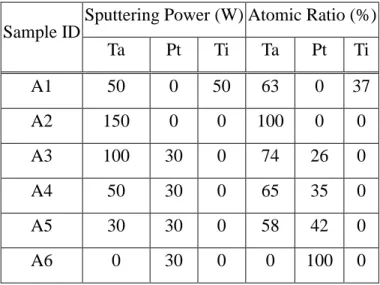
A simple MOS structure was fabricated to characterize the binary alloy systems. The starting material was (100)-oriented phosphorus doped Si wafer. Following standard RCA cleaning, gate oxide of 11 nm thick was thermally grown. The gate electrodes were patterned using the lift-off process. TaxPty and TaxTiy alloys were co-sputtered to a thickness of 60 nm on patterned photo-resist. Table 2-1 lists the deposition conditions and the atomic composition analyzed with Rutherford Backscattering Spectroscopy (RBS). After gate patterning, samples were annealed in N2 ambient at 400, 500, and 600℃ for 30 min followed by Al deposition at the back.
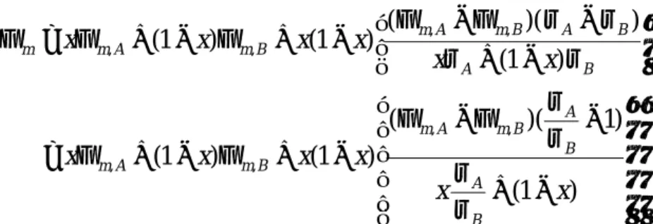
− + − Φ − Φ − + Φ − + Φ = − + − Φ − Φ − + Φ − + Φ = Φ ) 1 ( ) 1 )( ( ) 1 ( ) 1 ( ) 1 ( ) )( ( ) 1 ( ) 1 ( , , , , , , , , x x x x x x x x x x x x B A B A B m A m B m A m B A B A B m A m B m A m m ρ ρ ρ ρ ρ ρ ρ ρ
, where Φm,A and Φm,B are the pure constituent work functions of A and B, respectively, and ρA and ρB are the pure constituent total densities of states [14]. The density of states at Fermi energy ρ(εF) is proportional to the electronic specific heat constant
T k
Ce 2 ( F) B2
3
1π ρ ε
= , where kB is Boltzmen constant and T is temperature. In the case of
Ce,A/Ce,B~1, the Φm changes with x linearly as φ(x)= φB+x(φA-φB) [15]. The Ce values of Pt, Ta, and Ti are 6.8, 5.9, and 3.35 mJ/mole/K2, respectively [16]. Since the Ce values of Ta and Pt are very close, a nearly linear correlation can be expected.
The approximate work function (Φm,app) of annealed samples was extracted by comparing the measured C-V curves with the theoretical C-V curve [9, 13]. The Φm,app is defined as Fm,app.= Fm – Qss/Cox, where Qss is effective oxide charges and Cox is capacitance at accumulation mode. As the gate oxide thickness is 11 nm, a Qss of 1x1011 cm-2 results in aFm deviation of 0.05eV only. Fig. 2-1 shows the extractedFm,app of 400℃ annealed samples. The Qss of poly-Si gate devices is around 5x1010 cm-2. The Qss of metal gate devices might be higher than that of poly-Si gate. However, since the interface state density (Dit) of metal gate devices is similar to that of poly-Si gate, it is believed that the Qss of metal gate will not be much higher than that of poly-Si gate. Therefore, the Fm,app should be very close to the Fm. With increasing contents of high Fm elements, Pt in Ta-Pt alloys or Ta in Ta-Ti alloy, theFm,app shifts toward higher value. The Ta0.63Ti0.37 alloy and Ta0.58Pt0.42 alloy show Φm,app of about 4.16eV and 5.05 eV and is suitable for NMOSFETs and PMOSFETs, respectively. As expected, the Φm,app can be modulated continuously by adjusting the atomic composition of the alloy. This property allows for the use of the alloy system to obtain precise work function. For example, fully-depleted SOI devices require Φm of close to 4.6 eV [17], and can be achieved using the alloys with Ta/Pt ratio close to 0.74/0.26.
annealing at 600℃ is less than 1%, i.e. less than 0.1nm. These results imply that the alloys are thermally stable up to 600℃ on SiO2. This temperature is high enough for replacement gate process and is better than most of low work function elemental metals such as Ti [18].
Fig. 2-3(a) shows that the Φm,app decreases slightly with the increase of annealing temperature. Since the alloys are thermally stable on SiO2, this phenomenon cannot be attributed to the interaction between alloy and oxide. Fig.2-3(b) shows that the Dit also increases with the increase of annealing temperature. It is thus postulated that the decrease of
Φm,app comes from the thermal stress generated oxide charges. To reduce the effect of thermal stress, a stack gate electrode of W(50nm)/Ta-Pt(10nm) is proposed. The thermal expansion coefficient of W (4.4x10⁻⁶℃-1
) is lower than that of Pt (9.0x10⁻⁶ ℃-1) and Ta (6.6x10⁻⁶℃-1 ) and is close to that of Si (2.4x10⁻⁶℃-1
). Another benefit of using stack structure is that the resistivity of W (5.3x10⁻⁶ ohm-cm) is much lower than the resistivity of alloys (> 300x10-6ohm-cm). In this structure, the Ta-Pt alloy determines the work function and the W layer serves as the main conducting material.
Fig.2-4 shows the C-V characteristics of W(50nm)/Ta-Pt(10nm)/HfO2(5nm)/p-type Si structure after annealing at 600℃ and 800℃ in N2 ambient for 30 minutes. The apparent kink in the curve of 600℃ annealed sample points to the insufficient passivation of interface states at the HfO2/Si interface. The smaller kink and negligible hysteresis phenomenon of the 800℃ annealed sample imply that the stack structure is stable up to 800℃. The reduction of kink and hysteresis also confirms that thermal stress can be reduced by the stacked metal gate. The flatband voltage difference between 600 and 800℃ annealed devices may be attributed to the reduction of Qss and/or the change of Φm due to interaction between W and Ta-Pt or between Ta-Pt and HfO2. A 900℃ annealing distorts the C-V characteristic. The stability of metal gate/high K dielectric system is under investigation.
2-4 Conclusions
This work explores the characteristics of the binary alloys Ta-Pt and Ta-Ti for gate electrode application. With a proper composition of high and low work function metals, the work function of the metal alloys can be modulated from 4.16eV to 5.05eV continuously. The
To implement metal gate into CMOS process is tough not only for alloy gates. Metal gates for NMOS and PMOS can be patterned separately [19]. Using metal ion implantation to form various alloys is another choice; it depends on the maturity of metal ion implantation technology. However, gate electrode with work function near mid-gap of Si should be used for FD-SOI. The proposed alloy system shows the advantage of precise work function control in this aspect.
References
[1]. C. Y. Wong, J. Y. C. Sun, Y. Taur, C. S. Oh, R. Angelucci, and B. Davari, “Doping of n+ and p+ polysilicon in a dual-gate process”, in IEDM Tech. Dig., pp.238-241, 1988. [2]. J. R. Pfiester, F. K. Baker, T. C. Mele, H. H. Tseng, P. J. Tobin J. D. Hayden, J. W.
Miller, C. D. Gunderson, and L. C. Parrillo, “The effects of boron penetration on p+ polysilicon gates MOS devices”, IEEE Trans. Electron Devices, ED-37, No.8, pp.1842-1851, 1990.
[3]. S. H. Lo, D. A. Buchanan, Y. Taur, and W. Wang, “Quantum-mechanical modeling of electron tunneling current from the inversion layer of ultra-thin-oxide nMOSFETs”,
IEEE Electron Device Lett., vol.18, No.5, pp.209-211, 1997.
[4]. Y. Taur, D. Buchanan, W. Chen, D. J. Frank, K. I. Ismail, S.-H. Lo, G. A. Sai-Halasz, R. G. Viswanathan, H.-J. C. Wann, S. J. Wind, and H.-S. Wong, “CMOS scaling into the nanometer regime”, Proc. IEEE, vol.85, No.4, pp.486-504, 1997.
[5]. Y. Taur, C. H. Wann, and D. J. Frank, “25nm CMOS design consideration”, in IEDM
Tech. Dig. pp.789-792, 1998.
[6]. Q. Lu, Y. C. Yeo, P. Ranade, H. Takeuchi, T. J. King, C. Hu, S. C. Song, H. F. Luan, and D. L. Kwong, “Dual-metal gate technology for deep-sub-micron CMOS transistor”, in
Proc. Symp. VLSI Technology, pp.72-73, 2000.
[7]. H. Wakabayashi, Y. Saito, K. Takeuchi, T. Mogami, and T. Kunio, “A dual-metal gate CMOS technology using nitrogen-concentration-controlled TiNx film”, IEEE Trans. Electron Devices, ED-48, No.10, pp.2363-2369, 2001.
[8]. Y. S. Suh, G. Heuss, H. Zong, S. N. Hong, and V. misra, “Electrical characteristics of TaSiN gate electrodes for dual gate Si-CMOS devices”, in Proceedings of the IEEE
Symposium on VLSI Technology, pp. 47-48, 2001.
[9]. R. lin, Q. Lu, P. Ranade, T. J. King, and C. Hu, “An adjustable work function technology using Mo gate for CMOS devices”, IEEE Electron Devices Lett., vol.23, No.1, pp.49-51, 2002.
[10]. H. Zhong, S. N. Hong, Y. S. Suh, H. lazar, G. Heuss, and V. Misra, “Properties of Ru-Ta alloys as gate electrodes for NMOS and PMOS silicon devices”, in IEDM Tech. Dig.
[12]. I. Polishchuk, P. Ranade, T. J. King, and C. Hu, “Dual work function metal gate CMOS transistors by Ni-Ti interdiffusion”, IEEE Electron Devices Lett., vol.23, No.4, pp.200-202, 2002.
[13]. B. Y. Tsui amd C. F. Huang, “Investigation of Cu/TaNx Metal Gate for Metal-Oxide-Silicon Devices”, to be published in J. Electrochem. Soc., Jan., 2003. [14]. C. D. Gelatt, Jr. and H. Ehrenreich, “Charge transfer in alloys:AgAu”, Phys. Rev. B,
vol.10, No.2, pp.398-415, 1974.
[15]. R. Ishii, K. matsumura, A. Sakai, and T. Sakata, “Work function of binary alloys”, Appl.
Surf. Sci., vol.169-170, pp.658-661, 2001.
[16]. C. Kittel, Introduction to Solid State Physics, 5th ed., pp.167, John Wiley & Sons, Inc., New York, 1976.
[17]. L. Chang, S. Tang, T.J. King, J. Bokor, and C. Hu, “Gate length scaling and threshold voltage control of double-gate MOSFETs”, in IEDM Tech. Dig., pp. 719-722, 2000. [18]. C. Y. Ting, M. Wittmer, S. S. Iyer, and S. B. Brodsky, “Interaction between Ti and
SiO2”, J. Electrochem. Soc., vol.131, No.12, pp.2934-2938, 1984.
[19]. Y. C. Yeo, Q. Lu, P. Ranade, H. Takeuchi, K. J. Yang, I. Polishchuk, T. J. King, C. Hu, S. C. Song, H. F. Luan, and D. L. Kwong, “Dual-metal gate CMOS technology with ultrathin silicon nitride gate dielectric”, IEEE Electron Devices Lett., vol.22, No.5, pp.227-229, 2002.
Table 2-1. Deposition conditions used in this work and atomic compositions of alloys analyzed with Rutherford backscattering spectroscopy (RBS)
Sputtering Power (W) Atomic Ratio (%) Sample ID Ta Pt Ti Ta Pt Ti A1 50 0 50 63 0 37 A2 150 0 0 100 0 0 A3 100 30 0 74 26 0 A4 50 30 0 65 35 0 A5 30 30 0 58 42 0 A6 0 30 0 0 100 0
4.0
4.2
4.4
4.6
4.8
5.0
5.2
5.4
n+ poly
37%Ti
63%Ta
100%Ta
26%Pt
74%Ta
35%Pt
65%Ta
42%Pt
58%Ta
100%Pt
Fig.2-1. Extracted approximate work function (Φm,app.) of 400℃ annealed samples.
Ec
Ev
F
m,app.Fig.2-2. Cross-sectional TEM micrographs of (a) Ta0.58Pt0.42/SiO2 structure and (b) Ta0.63Ti0.37/SiO2 structure after annealing in N2 ambient for 30 minutes at 600℃. No Interfacial reaction is observed.
Fig.2-3. (a) Approximate work function (Φm,app) and (b) interface state density (Dit) versus annealing temperatures.
0
1
2
3
4
5
6
300
400
500
600
700
Temperature (℃)
4.0
4.2
4.4
4.6
4.8
5.0
5.2
F
m,app.(V)
Dit (10
11cm
-2eV
-1)
(a)
(b)
Ta
0.58Pt
0.42Ta
0.74Pt
0.26Ta
0.63Ti
0.37Ta
0.58Pt
0.42Ta
0.63Ti
0.370.0
0.2
0.4
0.6
0.8
1.0
-2.0
-1.5
-1.0
-0.5
0.0
0.5
1.0
Voltage (V)
No
rmalized Capacitance
Fig.2-4. Capacitance-voltage characteristic of the Ta0.58Pt0.42/HfO2/p-Si sample after annealing at 600℃ and 800℃ in N2 ambient for 30 minutes.
Forward
Reverse
800℃
Chapter 3
Process Stability of Alloy Gate
3-1 Introduction
Metal gates are currently proposed to replace the poly-Si gate beyond 65nm technology node1 in order to solve the problems of poly-depletion and boron penetration [2-6]. However, before any metal gates can replace the poly-silicon gate, they must be able to be compatibly integrated into the process of MOSFET fabrication and should provide higher device performance than that of poly-silicon gate. To integrate the metal gate, there are two kinds of metal gate processes, the dummy gate process [7-10] (gate last process) and conventional gate process (gate first process) [11-13]. Compared with conventional processes, the dummy gate process has extra steps including the chemical-mechanical polishing (CMP) step and dummy-gate-removal so that the gate last process is more complicated [7-10]. Its main benefit is the lower temperature, which protects the thermal stability of metal gates since most metals may react with the gate dielectric at temperatures higher than 600°C. The temperature of the gate last process should be controlled to be lower than 500°C after the metal gate deposition. On the other hand, metal gates should withstand the high temperature of source/drain (S/D) activation process to be integrated with a relatively simple process of the conventional process [11-13]. The key factor for those metal gates is that they should be chemical inert as well as they should have the immunity to avoid dopant channeling during source/drain ion implantation [14, 15]. For device performance, metal gates should have proper work function (Fm) to obtain suitable threshold voltage for the n-type or p-type MOSFETs [16, 17]. The work function of metals must be 4.1-4.4eV for NMOSFETs and 4.8-5.1eV for NMOSFETs, respectively. In previous chapter, we showed how the work function of the binary metal alloys can be easily modulated to a suitable value for NMOSFETs or PMOSFETs by adjusting atomic ratios of the composition [18]. Moreover, a wide range of work functions should be available by the mixture of the two metal elements which contains a metal with much high work function, near the valence band of silicon, and a metal with quite low work function, near the conduction band of silicon, such as Ta-Pt alloys [18] or Ru-Ta alloys [19, 21]. In this
3-2 Experiments
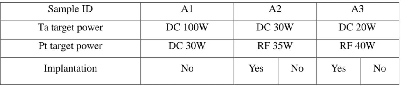
Simple MOS capacitors with gate electrodes of Ta-Pt alloys were fabricated on p-type Si wafers. The beginning is the 6-inch p-type (100) oriented silicon wafers. After wafer cleaning, the gate oxide was thermally grown to 6nm thick in dry-oxygen atmosphere at 900 °C. After gate oxidation, the metal gates would be completed by lift-off process. Metal gate patterns were first defined with a conventional lithography process. Then, the alloys were deposited in a co-sputtering system to 55nm thick, and the sputtering power of Ta and Pt targets were set to DC 30 and RF 35 watts, or DC 20 and RF 40 watts. The wafers were split and than some samples were implanted with 5e15 cm-2 dosage of arsenic ions (As+), phosphorous ions (P+), or boron di-fluoride ions (BF2+). After implantation, metal gates were finished by the lift-off process. Then, all MOS capacitors were capped with 60nm thick silicon nitride films which were deposited in a plasma-enhanced chemical vapor deposition (PECVD) system at 300 °C, in order to avoid out-gassing of impurities when the samples were annealed at high temperatures. Samples were annealed at temperatures between 400 and 800 °C in a rapidly thermal annealing (RTA) system for 30sec. Finally, the contact windows of gate electrodes were patterned by conventional lithography and wet etching process, and backside contacts were formed with an aluminum film deposited in a thermal evaporation system. The samples for the study of thermal stability was deposited with sputtering power of DC 100 watts and DC 30 watts for Ta and Pt targets, respectively, in order to form a Ta-rich alloy film, since Ta is more chemically reactive than Pt. Its annealing conditions of the higher thermal budget were from 400 °C to 800 °C in a horizontal furnace system for 30min. Table 1 lists the sample ID and conditions.
The X-ray photoelectron spectroscopy (XPS) was used to analysis the binding energy of Ta-Pt alloy. The Auger electron spectroscopy (AES) was used to detect the depth distribution of atomic composition of the alloy. The X-ray diffraction pattern was used to study the phase of the alloy. The secondary ion mass spectrometer (SIMS) was used to detect the distribution of implanted impurities before and after implantation. The flat band voltage (Vfb) was extracted from the C-V curves measured by Algient 4284 at 100 KHz. 24
the XPS for the A1 samples with Ta-Pt (6nm)/SiO2 (6nm)/Si structure. Figures 1(a) and 1(b) show the XPS spectra of O and Ta atoms, respectively. At the sample surface, the binding energy of 1s orbit of O atom is 531eV and that of 4f7/2 orbit of Ta atom shifts 1-2eV from that of the bulk Ta-Pt alloy and becomes 23eV, while the pure Ta would reveal 4f7/2 orbit signal at 21.5-22 eV. The large shift of Ta 4f7/2 orbit signal reflects a Ta-O bond. After short surface-sputtering periods of 100sec, 200sec, and so on, no obvious oxygen-related peaks are observed, and the peak of Ta atom is still at 23eV which comes from the Ta-Pt alloys. As seen in the 800°C samples, the binding energy of the bulk and interface region of alloy is all the same, and the lack of O 1s orbit signal indicates that the inner of Ta-Pt alloy is almost oxygen free. The Ta-O surface bond is attributed to the reaction of Ta atoms and the residual O2 molecules in the annealing ambient. The same binding-energy signals of Ta atoms within the alloy for 400 and 800 °C annealed A1 samples are detected as shown in Fig. 2. For any the annealing temperatures, the same binding energy should imply that a stable chemical bond of the alloy. The atomic composition of the Ta-Pt alloy is analyzed by the AES. In Fig.3, AES depth profile shows that the atomic composition of both Ta and Pt of the 400 and 800 °C annealed samples are almost constant, except at the sample surface. The AES signals at the surface are affected by the surface oxidation. Figure 4 shows the X-ray diffraction pattern of the Ta-Pt alloy. The patterns of the samples are almost the same below 700°C, and present the phases of ß-Ta (200) and Pt (100). By 800°C, the phase of Pt (200) is revealed. Regardless of annealing temperatures, the all observed phases belong to tantalum hexagonal crystallite or platinum cubic crystallite. Overall, the same binding energy, uniform composition, and stable micro-crystallite reflect that the Ta-Pt alloy is a highly thermally stable alloy up to 800°C. Furthermore, the absence of the phases of metal oxides and binding energy shift of tantalum implies that the alloy is also chemically stable on the silicon dioxide films.
3-3-2 Work function effect of the impurity incorporation
The work function effect of III or V impurity incorporation of the alloy is investigated by
the flat band voltage (Vfb) change. The Vfb is
ox eff ms fb C Q
V =Φ − , where Fms is the work function difference between metal gate and silicon substrate. Qeff and Cox are effective oxide charges and oxide capacitance, respectively. The variation of Vfb can reflect the change of
versus implantation conditions for 500°C and 800°C annealed samples. The ? Vfb is the difference of flat band voltage between implanted samples and un-implanted samples. The fabrication processes of those are almost the same, except for the implantation process. In Fig.5 (a) almost all the ? Vfb of the A2 samples are located at -0.05V, except for the 800°C samples implanted with 25KeV BF2+. Under all the implantation conditions, the difference of ? Vfb is generally less than 0.05V. Furthermore, the difference of the ? Vfb of all the 500°C and 800°C samples with the same implantation condition is less than 0.02V. The ? Vfb is almost independent of the implantation condition and annealing temperature. Similarly, Figure 5(b) shows that the ? Vfb of A3 samples are located approximately at -0.1V for 500°C samples and at -0.05V for 800°C samples. For all of implantation conditions, the difference of the ? Vfb is generally less than 0.05V. The difference of the ? Vfb for all the 500°C and 800°C samples with the same implantation conditions is also about 0.05V. Figure 6 shows the impurity depth distribution both before and after annealing A3 samples implanted with 40KeV As+ or 30KeV BF2+. In Fig. 6(a) the depth distribution of arsenic atoms of the before and after annealing A3 samples are almost the same. The abnormal peak signal of Ta comes form the SIMS detection error and it always occurs at the interface between metal gate and silicon dioxide. Compared with the Ta distribution, arsenic is free near the interface between metal gate and silicon dioxide. This presumes that the ? Vfb should not come from the work function change but mainly from oxide charges since the Ta-Pt alloy is free of impurities at the interface between the metal gate and silicon dioxide. Figure 6(b) shows that the boron impurities are distributed near the surface of the alloy before annealing. Subsequently, boron impurities are redistributed throughout the alloy film after 800°C annealing. In addition, the depth distributions both before and after annealing P+ implanted samples are also detected and are similar to those of BF2+ implanted samples. Although the impurities of boron or phosphorus can be diffused throughout the alloy films at 800°C, the ? Vfb of both A2 samples and A3 samples are still small. This confirms that the work function of the alloys incorporated with impurities of boron or phosphorus should be almost constant. The C-V characteristics of 800°C A3 samples are shown in Fig. 7. The C-V curves of the As+ and P+ implanted samples are smoother than those of the BF2+ implanted and un-implanted samples. This confirms that the ? V should be due to the oxide charge, which might be caused by the sputtering damage
impurity could be 8.3E20 cm-3 if the distribution of impurities is uniform. The impurity concentration can only cause a ? Vfb less than 0.1V, which should be mostly caused by oxide charges. Moreover, the dosage for implantation process of MOSFET fabrication would generally be less than 5E15 cm-2 so that the work function variation of the alloy gate affected by the impurities should be much less than 0.1V and could be neglected. In other words, this implies that the alloys are immune to impurities due to implantation.
3-4 Conclusions
The Ta-Pt alloy with tunable work function is a potentially suitable material for metal gates due to its thermal stability and resistance to the impurities. It could be integrated in the conventional MOSFET process, and the work function should not be changed by the incorporation of the implantation impurities of arsenic ions, boron ions and phosphorus ions. Therefore, the control of threshold voltage of the alloy-gate MOSFET could be easier, and not be disturbed by the S/D implantation process.
References
[1]. International Technology Roadmap for Semiconductors (ITRS) 2003 Edition, Semiconductor Industry Association (SIA), http://public.itrs.net
[2]. B. Yu, D. H. Ju, N. Kepler, T. J. King, and C. Hu, in Proceedings of the IEEE
Symposium on VLSI Technology1997, p.105
[3]. K. Chen, M. Chan, P. K. Ko, C. Hu, and J. H. Huang, Solid-State Electron, 38, 1975
(1995).
[4]. N. D. Arora, R. Rios, and C. L. Huang, IEEE Trans. Electron Devices, ED-42, 935(1995).
[5]. The International Technology Roadmap for Semiconductors, p.123, Semiconductor Industry Association, San Jose, CA (1999).
[6]. J. R. Pfiester, F. K. Baker, T. C. Mele, H. H. Tseng, P. J. Tobin J. D. Hayden, J. W. Miller, C. D. Gunderson, and L. C. Parrillo, IEEE Trans. Electron Devices, ED-37, 1842(1990).
[7]. J. Pan, C. Woo, M.-V. Ngo, P. Besser, J. Pellerin, Q. xiang, and M.-R. Lin, IEEE
Electron Device Lett. Vol. 24, 547 (2003)
[8]. J. Pan, C. Woo, M.-V. Ngo, C.-Y. Yang, P. Besser, P. King, J. Bernard, E. Adem, B.Tracy, J. Pellerin, Q. xiang, and M.-R. Lin, IEEE Electron Device Lett. Vol. 50, 2456 (2003) [9]. C. Ren, H. Y. Yu, J. F. Kang, x. P. Wang, H. H. H. Ma, Y.-C. Yeo, D. S. H. Chan, M._F.
and Li D.-L. Kwong IEEE Electron Device Lett. Vol. 25, 580 (2004)
[10]. Chatterjee, R. A. Chapman, G. Dixit, J. Kuehne, S. Hattangady, H. Yang, G.A. Brown, R. Aggarwal,U. Erdogan, Q. He, M. Hanratty, D. Rogers, S. Murtaza, S.J. Fang, R. Kraft, A.L.P. Rotondaro, J.C. Hu, M. Terry, W. Lee, C . Fernando, A. Konecni, G. Wells, D. Frystak, C. Bowen, M. Rodder, and I.-C. Chen, in Proceedings of IEDM 1997, p.832 [11]. Chang Seo Park, Byung Jin Cho, and Dim-Lee Kwong, IEEE Electron Device Lett. Vol.
24, 298 (2003)
[12]. HongYu Yu, Ming-Fu Li, Senior and Dim-Lee Kwong, IEEE Trans. Electron Devices,
ED-51, 609(2004).
Devices, ED-31, 1174(1984).
[15]. S.-I. Ohfuji, C. Hashimoto, T. Amazawa, and J. Murota, J. Electrochem. Soc.:
Solid-State science and Technology, p.446(1984)
[16]. Q. Lu, Y.-C. Yeo, P. Ranade, H. Takeuchi, T.-J. King, and C. Hu, in Proceedings of the
IEEE Symposium on VLSI Technology 2000, p 72-73
[17]. B. Cheng, B. Matti, S. Samayedam, J. Grant, B. Taylor, P. Tobin, and J. Mogab, in
Proceedings of IEEE Intl. SOI Conf., 2001 p.91
[18]. B.-Y. Tsui and C.-F. Huang, IEEE Electron Device Lett., vol. 24, p. 153 (2003)
[19]. H. Zhong, S.-N. Hong, Y.-S. Suh, H. Lazar, G. Hcuss, and V. Misra, in IEDM Tech. Dig.,
2001, p.467
[20]. V. Misra, H. Zhong; H. Lazar,Electron IEEE Electron Device Lett., vol. 23, p.354 (2002)
[21]. J. Lee, H. Zhong, Y.-S. Suh; G. Heuss, J. Gurganus, B. Chen, V.Misra, in IEDM Tech.
Dig., 2002, p.359
[22]. C.-F. Huang and B.-Y. Tsui , in Proceedings of the Iinternational Conference on
Microelectronics (MIEL)2004, vol. 2, p.451
[23]. B. C. Giessen, R. H. Kane, and N. J. Grant, Trans. Met. Soc. AIME, Vol.233, p.855 (1965)
[24]. D. K. Schroder, Semiconductor Material and device Characterization 2nd ed., p.347, John Wiley & Son, New York(1998)
Table 3-1. Sample ID and conditions
Sample ID A1 A2 A3
Ta target power DC 100W DC 30W DC 20W
Pt target power DC 30W RF 35W RF 40W
20
22
24
26
28
30
Binding Energy (eV)
surface 100sec 200sec 300sec 400sec 500sec surface 100sec 200sec 300sec 400sec 500sec Ta-Pt Si surface 100sec 200sec 300sec 400sec 500sec Ta-Pt Si Ta 4f5/2 Ta 4f7/2525
527
529
531
533
535
Binding Energy (eV)
surfdace
100sec
200sec
300sec
400sec
500sec
O 1s
525
527
529
531
533
535
Binding Energy (eV)
surfdace
100sec
200sec
300sec
400sec
500sec
O 1s
20
22
24
26
28
30
Binding Energy (eV)
A1-400℃-200sec
A1-800
℃-200sec
Ta 4f
5/2Ta 4f
7/2Fig.3-2. The binding energy of Ta atoms of the 400 °C and 800 °C annealed A1 samples detected by XPS after Ar surface sputtering for 200sec.
0
500
1000
1500
2000
Time (sec)
Counts (a.u.)
Ta-400℃
Ta-800℃
Pt-400
℃
Pt-800℃
Fig.3-3. Depth distribution of the compositions of the 400 °C and 800 °C annealed A1 samples detected by AES.
25
30
35
40
45
50
55
2 Theta (degree)
Fig.3-4. X-ray diffraction pattern of the A1 samples after 400°C, 500°C, 600°C, 700°C, and 800°C annealing.
400°C
500°C
600°C
700°C
800°C
ß-Ta(212) Pt(100)
Pt(200)
-0.15
-0.1
-0.05
0
0.05
0.1
0.15
As/30KeV
P/15KeV
BF2/25KeV
△
Vfb
A2-500
A2-800
Δ
V
fb(V)
P
+/15KeV
BF
2+/25KeV
As
+/30KeV
-0.15
-0.1
-0.05
0
0.05
0.1
0.15
As/40KeV
P/20KeV
BF2/30KeV
△
Vfb
A3-500
A3-800
Δ
V
fb(V)
P
+/20KeV
BF
2+/30KeV
As
+/40KeV
Fig.3-5. The flat-band voltage shift (? Vfb) of (a) A2 samples; (b) A3 samples with various implantation conditions after 500°C and 800°C annealing. The ? Vfb value is the
1.0E+00
1.0E+01
1.0E+02
1.0E+03
1.0E+04
1.0E+05
1.0E+06
0
0.05
0.1
0.15
0.2
Depth(um)
Counts (a.u.)
As-implant. Ta
As-implant. As
After ann. Ta
After ann. As
Ta
+before ann.
As
+before ann.
Ta
+after ann.
As
+after ann.
Ta
+As
+1.0E+00
1.0E+01
1.0E+02
1.0E+03
1.0E+04
1.0E+05
1.0E+06
0
0.05
0.1
0.15
0.2
Depth (um)
Counts (a.u.)
As-implant. Ta
As-implant. B
After ann. Ta
After ann. B
Ta
+before ann.
B
+before ann.
Ta
+after ann.
B
+after ann.
B
+Ta
+0.0E+00
2.0E-01
4.0E-01
6.0E-01
8.0E-01
1.0E+00
1.2E+00
-2
-1
0
1
Vg (V)
Capacitance (F)
A3-800
As/40KeV
P/20KeV
BF2/30KeV
P
+/20KeV
BF
2+/30KeV
As
+/40KeV
W/O Implant
A3 sample
800°
C
Fig.3-7. C-V characteristic of 800°C annealed A3 samples with and without implantation process.
Chapter 4
Metal Nitride Gate Technology – MoN
4-1 Introduction
Molybdenum nitride (MoNx) is a material with rigid, inert and corrosion-resistant characteristics [1-5]. This material also has good thermal stability. Such characteristics of MoNx are very attractive to the applications of semiconductor industry. The work-function of Mo is about 4.6V and possesses large modulation ability (4.2-4.9V) on different dielectrics. Due to the work-function of 4.8V for Mo on SiO2, this metal can be the metal gate material of PMOS and its work function could be modulated by changing the nitrogen content in MoNx. Finally, the threshold voltage could also be adjusted by work function modulation.
In this chapter, we discuss the work function modulation and thermal stability of MoNx with different ratio of nitrogen, and study physical mechanism of MoNx work-function modulation by physical analysis. Besides, the phenomenon of sputter damage during process would be investigated later.
4-2 Results and Discussion
4-2-1 Physical characteristics of MoNx
The atomic ratio of MoNx could be detected by RBS. Fig.4-1 shows the RBS spectrums of MoNx with three different N/Mo ratios. In order to clearly distinguish the signals of C, N, and Mo, carbon substrate was used as the sample substrate. Resolution of atomic ratio from RBS is about 0.05. Theoretic values of N/Mo atomic ratios for MoN-1, MoN-2, and MoN-3 are 0.85, 1.0, and 1.45, respectively. MoN-0 stands for the pure metal of Mo.
Fig.4-2(a)-(c) were grazing-angle XRD spectrums of MoN-1, MoN-2 and MoN-3 after annealing with various temperature. After 400℃annealing, spectrum of MoN-1 showed peaks of MoN(200) and MoO3(110). The peak intensity of MoN(200) strongly increased with the annealing temperature, but that of MoO3(110) relatively decreased. Besides, there was no change of phase and orientation for MoN-1 as the annealing temperature increased. Compared
crystallization enhanced after 600℃ annealing, so MoN(200) peak appeared clearly. For MoN-3 whose nitrogen ration was 20/20, the diffraction peak of MoN(200) come out apparently until 800℃ annealing. The MoO3(110) peak at 2θ =23.34° was signal of surface oxidation during sputtering. Its intensity was very weak and increased slightly with the nitrogen ratio.
The stress of MoNx after annealing was about 1.2GPa tensile (Fig.4-3). And after the adhesion test of MoNx film, the crack of Si substrate indicated that MoNx film had superior adhesion with SiO2 and HfO2 dielectrics.
4-2-2 Electrical Analysis of MoNx
A. Sheet-Resistance Measurement
Fig.4-4(a) was the sheet resistance of as-deposit MoNx films with different nitrogen content. And Fig.4-4(b) was the sheet resistance with different nitrogen contents and various RTA temperature from 400℃ to 800℃. The resistivity was normalized to the value at 400℃. From Fig.4-4(a) resistance increased apparently as the ratio of Ar/N2 was larger than 20/10 owing to the apparent increase of nitrogen content in MONx. And Fig.4-4(b) showed that resistivity decreased with the annealing temperature below 600℃. From XRD data, this could be due to the enhancement of crystallization caused by the increase of annealing temperature. As annealing temperature was higher than 800℃, resistivity abruptly increased without other bonds production and color change. Further study is needed for he fact that samples with over saturated nitrogen showed high resistivity after 700℃ annealing.
B. Sputtering Damage Analysis
As shown in Fig.4-5(a), films deposited with higher power showed larger SiO2 dielectric leakage current. K. Nakajima described that high energy metal atom during sputtering would bump into the dielectric and caused sputter damage [6]. Compared with the I-V curve [Fig.4-5(b)], it seems that film with higher sputtering power shows severe sputter damage. We deposited films with three different powers upon two kinds of dielectric and investigate films by ICP-MS to find the suitable sputtering power.
decreases. Because the atomic resolution of Mo for ICP-MS is 0.2ppb [3x10¹⁷(atom/ 3
cm )], the measured concentration below the resolution is considered lower Mo concentration. The detected concentration is below the resolution at the power of 25W and this means no sputter damage existed on the SiO2 surface. For HfO2 dielectric, the surface atomic concentration of Mo is below the resolution. So sputter damage doesn’t exist on HfO2 films. This ability of anti-sputter damage could be due to that HfO2 has higher density and mass than SiO2.
Sputtering process would cause damage of SiO2 in traditional process, and increase leakage current and surface trap charge. But HfO2 dielectric used in the next generation has the ability of anti-sputter damage. So it’s worthy to discuss that if sputtering process could be taken into new transistor process. Of course, further reliability analysis is still needed to be investigated.
C. C-V characteristics and thermal stability of MoNx
Fig.4-7 (a)-(d) are C-V curves of MoN-0、MoN-1、MoN-2 and MoN-3 deposited on 40nm SiO2 versus various different annealing temperature. Each C-V curve was averaged by measuring at least 10 capacitances. MoN-0 which was capacitance with pure Mo metal gate was very stable and not affected by annealing temperature (Fig.4-7). Slight distortion in accumulation mode was observed for MoN-1 which annealing below 600℃ and this was probably due to the increase of sputter damage induced interface trap. After 600℃ annealing, these interface traps were recovered. Then the measured CV curve was more normal.
The CV curves of MoN-2 after 400℃ and 500℃ annealing had slight flat-band voltage shift of about 0.1V. From XRD spectrums, this could be due to the different crystallization extent of MoNx. The flat-band voltage shift was only about 40mV when annealing temperature was higher than 500℃. This was due to that the crystallization reached stable. The slight distortion like MoN-1 was happened when annealing temperature was lower than 600℃, and this situation could be improved by high temperature annealing. The CV curve of MoN-3 showed that the shift of CV curve was not obvious as increasing annealing temperature. According to XRD analysis results, it would have obviously crystallization as annealing temperature was up to 800℃.
between HfO2 and SiO2. Fig.4-10 was the plot of flat-band voltage shifts compared with that of 400℃. The Vfb shift of MoNx on HfO2 was very stable with annealing temperature (Fig.4-10). From above we could know that MoNx film has a good thermal stability whether on SiO2 or on HfO2 dielectrics.
D. Work-Function Modulation of MoNx
For the sample of 500℃ annealing, the curve of average Vfb versus capacitance effective thickness (CET) with various SiO2 thickness was shown in Fig.4-11 and Fig.4-12 was curve of Vfb versus CET with various SiO2 thickness for HfO2/SiO2 structure. From Fig.4-11, the slopes of MoN-0, MoN-1, MoN-2 and MoN-3 are nearly parallel and conform to constant total charge. When ratio of nitrogen flow rate increases, CV curves shift rightward and Vfb shift upward. And it seems to get saturate when the ratio is over 20/10, thus Vfb of MoN-3 is a bit higher than that of MoN-2. The slopes of CV curve for MoN-2 and MoN-3 from Fig.4-12 are different from two others. H. Kattelus stated that nitrogen could release the stress of MoN, lower interfacial trap density and get larger slope [7]. The shift of CV curves seems to get affected by saturation of nitrogen and tends to a constant value finally. Compared Fig.4-11 with Fig.4-12, the latter get 0.3V higher Vfb than the former.
The work function could be extracted from Vfb of different oxide thickness. Fig.4-13 and Fig.4-14 are figures of work function versus different thickness of SiO2 and HfO2/SiO2 with different annealing temperature, respectively. The Vfb of each thickness of the same annealing temperature was taken the average of several values. From Fig.4-13, the work functions of MoN-0, MoN-1, MoN-2 and MoN-3 at 500℃ annealing were 4.6V, 4.97V, 5.03V and 5.11V respectively. The work function increases with the ratio of nitrogen flow rate, and finally saturates to a constant value until the ratio of flow rate larger than 20/10. The modulation of work function changes from 4.97V to 5.11V as the ratio of N/Mo is from 0.85 to 1.45. Range of modulation is 0.14V. Besides, work function slightly increases about 40mV with annealing temperature. This is due to the higher crystallization structure of MoNx from the prior results of XRD and CV analysis.
For structure of HfO2/SiO2 stack, work functions of MoN-0, MoN-1, MoN-2 and MoN-3 have a value about 4.89V, 5.31V, 5.41V and 5.37V respectively. These values are higher than those of SiO2. The work function tends to a constant value as nitrogen saturates. The
It’s worthy to discuss that the work function of MoNx on HfO2 is 0.3V higher than that on SiO2. The Fermi level pinning caused by dipole layer screening effect of High-κ materials like HfO2 limits metal work function to the mid-gap of Si. Then work function of metal gate on P substrate should reduce. But our results didn’t fit the fact. From the comparison of MoN-0 and MoN-3, the difference was independent of the kinds of oxide dielectric. So MoN on HfO2 dielectric should have no problem about Fermi level pinning.
,
1
'
1*
ms ms it High oxEOT
Q
κφ
φ
ε
−=
−
(4-1)The difference of 0.3V might come from the methods of work function extraction. The assumptions are HfO2/SiO2 interfacial trap density of 5*1012cm-2 and very thin HfO2 thickness. But actually the trap density is higher than that of our assumption. According to Eq 4-1, R. Jha presented that Qit High-? is negative when Qit SiO2 is positive [8]. When work function is -0.3V and ? value is 5, the value of Qit High-? equals 1.65*10
13
cm-2, higher than the value of our assumption.
4-3 Summary and Conclusions
We investigated characteristics of MoNx like thermal stability and work function modulation with different ratio of nitrogen. Then we understood the physical mechanism of work function modulation by physical analysis. According to the analysis of RBS, the ratios of N/Mo of MoNx are 0.85, 1.0 and 1.45. Several important characteristics are described below:
1. The main phase and orientation of MoN-1, MoN-2 and MoN-3 is MoN(200). As the raise of N/Mo ratio, amorphous phase occurs and resistivity becomes higher. The phase and orientation remains with the increase of annealing temperature, and crystallization becomes enhance obviously.
2. High-? HfO2 with metal gate has highly resistance to sputter damage and doesn’t react with MoNx.
The modulation range of work function can be up to 0.4V from pure Mo to MoN of N/Mo ratio 1.57 and this would be useful for threshold voltage adjustment. In aspect of process temperature, the nitrogen can’t be too much and saturates in order to avoid the affect of thermal stability. The over high sheet resistance seems to be the common problem of nitride and this could be the limiting condition for metal nitride to be the candidate of metal gate. This situation of high resistivity could be solved by stack another layer of low resistance metal upon metal nitride to reduce the sheet resistance.
Besides, Fermi level pinning effect was found for the metal gate on HfO2 dielectric and moved the Fermi level toward the mid-gap of Si. Then Fermi level would be pinned there. This effect caused that the needed value of work function would be larger than theoretical value. But from our work (Fig.4-13 and Fig.4-14), difference of work functions between MoN-0 and MoN-3 on SiO2 and HfO2 doesn’t get affected by oxide layer. So Fermi level pinning effect seems not happen. This situation should be worthy to notice.
References
[1]. G. Wei, “ Trandition Metal Nitride Functional Coatings”, JOM. September 2001.P. Ranade, Y. K. Choi, H. Daewon, A. Agarwal, M. Ameen, and T. J. King,” Tunable work function molybdenum gate technology for FDSOI-CMOS”, IEDM 2002, p. 363.
[2]. R. Lin, Q. Lu, P. Ranade, T.-J. King, and C. Hu, “An adjustable work function technology using Mo gate for CMOS devices”, IEEE Electron Device Letters, VOL. 23, No. 1, Jan. 2002.
[3]. P. Ranade, H. Takeuchi, T.-J. King, and C. hu, “Work Function Engineering of Molybdenum Gate Electrodes by Nitrogen Implantation”, Electrochemical and Solid-State Letters, 4 (11) G85-G87 (2001).
[4]. M. J. Kim, D. M. Brown, and W. Katz, “Molybdenum nitride film formation”. Electrochem. Soc., Vol. 130, p. 1196, 1983.
[5]. K. Nakajima, Y. Akasaka, and M. Kaneko, “Work Function Controlled Metal Gate Electrode on Ultrathin Gate Insulators”, 1999 Symp. VLSI Tech.
[6]. H. Kattelus, J. Koskenala, A. Nurmela, and A. Niskanen, “Stress control of sputter-deposited Mo-N films for micromechanical applications”, Microelectronic Engineering 60 (2002) 97-105.
[7]. R. Jha, J. Gurganos, Y. H. Kim, R. Choi, and J. Lee, “ A Capacitance-Based Methodology for Work Function Extraction of Metal on High-?”. IEEE EDL, VOL. 25, No. 6, JUNE 2004.
0 500 1000 1500 2000 0 500 1000 1500
Mo
MoN-2 MoN-1C
MoN-3N
Normalize Yeild
ChannelFig.4-1. RBS spectrum of MoNx on carbon substrate.
Ratio of Ar/N2 flow rate: MoN-1=20/5,MoN-2=20/10,MoN-3=20/20 Ratio of N/Mo: MoN-1=0.85,MoN-2=1.0,MoN-3=1.45
20 30 40 50 60 As-depo WN(100) WO 3 (001) 800oC 400oC 600oC
Intensity(a.u.)
2? (deg.) 20 30 40 50 60 As-depo WN(100) WO 3 (001) 800oC 400oC 600oCIntensity(a.u.)
2? (deg.)20 30 40 50 60 As-depo WN(100) WO 3 (001) 800oC 400oC 600oC
Intensity(a.u.)
2? (deg.)Fig.4-2. (a) XRD spectrum of MoN-1 with different annealing temperature. (b) XRD spectrum of MoN-2 with different annealing temperature. (c) XRD spectrum of MoN-3 with different annealing temperature
0 100 200 300 400 500 0.6 0.8 1.0 1.2 1.4 1.6 1.8 tensile 1st ramp 2nd ramp
Stress(GPa)
Temperature(
OC)
0.40 0.45 0.50 0.55 0.60 0.65 600 800 1000 1200 1400 1600 1800 MoN-2 MoN-3 MoN-1
Resistence
(µΩ
-cm)
N/Mo atomic ratio
400 500 600 700 800 0.6 0.8 1.0 1.2 1.4 1.6 1.8 MoN-1 MoN-2 MoN-3
Normalize R
sN/Mo atomic ratio
Fig.4-4. (a) Sheet resistance of as-deposit 60nm MoNx film and (b) sheet resistance of the 60nm MoNx after annealing at different temperatures.
0
2
4
6
8
10
10
-111x10
-91x10
-71x10
-51x10
-31x10
-11x10
1 1 1 1 1 1 1J(A/cm
2)
Vg(Volt)
MoN/SiO2-100W MoN/SiO2-50W MoN/SiO2-25W MoN/HfO2-100W MoN/HfO2-50W MoN/HfO2-25wFig.4-5. (a) I-V curve of different sample structures of our work and (b) I-V curve of sputter damage from literatures.
1.0 1.5 2.0
10
1910
20 1-2 nm 0-1 nm 1-2 nm DC power=100W DC power=50W DC power=25WConcentration(cm
-3)
Depth
1.0 1.5 2.010
1610
17 1-2 nm 1-2 nm 0-1 nm DC power=100W DC power=50W DC power=25WConcentration(cm
-3)
Depth
Fig.4-6. (a) ICP-MS plot of MoN/SiO2 structure. The surface concentration of 1020(cm-3) means that sputter damage exists. (b) ICP-MS plot of MoN/HfO2 structure. The surface concentration is below the resolution value. This means that sputter damage doesn’t exist. The resolution of ICP-MS is 3*1017(cm-3).
-3 -2 -1 0 1 2 0 20 40 60 80 100 120 400O C 500OC 600O C 700OC 800O C C(pF) V(Volts) -2 -1 0 1 2 0 20 40 60 80 100 120 400OC 500OC 600O C 700OC 800OC C(pF) V(Volts) -2 -1 0 1 2 3 0 20 40 60 80 100 120 140 400OC 500OC 600O C 700OC 800OC C(pF) V(Volts) -2 -1 0 1 2 20 40 60 80 100 120 400OC 500OC 600O C 700OC 800OC C(pF) V(Volts)
Fig.4-7. CV curves of MoNx/SiO2 versus various annealing temperatures. (a)MoN-0; (b)MoN-1; (c)MoN-2; (d)MoN-3.
400 500 600 700 800 -0.10 -0.05 0.00 0.05 0.10 MoN-0 MoN-1 MoN-2 MoN-3
∆
V
FB(V)
Temperature(
OC)
-3 -2 -1 0 1 2 20 40 60 80 100 120 C(pF) V(Volts) 400OC 500OC 600OC 700OC 800O C -2 -1 0 1 2 20 40 60 80 100 120 400O C 500O C 600OC 700OC 800OC C(pF) V(Volts) -2 -1 0 1 2 20 40 60 80 100 120 400OC 500O C 600OC 700OC 800OC C(pF) V(Volts) -2 -1 0 1 2 20 40 60 80 100 120 400OC 500O C 600OC 700OC 800OC C(pF) V(Volts)
Fig.4-9. CV curves of Mo/ HfO2(5nm)/SiO2 (40nm) versus different annealing temperatures. (a)MoN-0; (b)MoN-1; (c)MoN-2; (d)MoN-3.
![Table 7-1. Material properties of HfO 2 , ZrO 2 , and Al 2 O 3 [22]. Property Aspect HfO 2 ZrO 2 Al 2 O 3 Band-gap(eV) 5.68 5.16 8.3 Barrier height to Si(eV) 1.6 1.5 2.9 Dielectric constant 25~40 ~25 8~10 Dielectric strength (MV /cm) 2~4](https://thumb-ap.123doks.com/thumbv2/9libinfo/8745958.205002/116.892.135.762.198.855/material-properties-property-barrier-dielectric-constant-dielectric-strength.webp)