國 立 交 通 大 學
電子物理研究所
博 士 論 文
介觀物理下的兩個主題之
壹: 顆粒鉻薄膜的電導率及穿隧電子能態密度
貳: 單重態自旋電子在量子點中的自旋阻滯
Two topics on mesoscopic electron transport
Part I:Conductivity and tunneling density of states in granular Cr films
Part II:Spin blockade with spin singlet electrons
研 究 生:孫羽澄
指導教授:林志忠 教授
國 立 交 通 大 學
電子物理研究所
博 士 論 文
介觀物理下的兩個主題之
壹: 顆粒鉻薄膜的電導率及穿隧電子能態密度
貳: 單重態自旋電子在量子點中的自旋阻滯
Two topics on mesoscopic electron transport
Part I:Conductivity and tunneling density of states in granular Cr films
Part II:Spin blockade with spin singlet electrons
研 究 生:孫羽澄
指導教授:林志忠 教授
介觀物理下的兩個主題之
壹: 顆粒鉻薄膜的電導率及穿隧電子能態密度
貳: 單重態自旋電子在量子點中的自旋阻滯
Two topics on mesoscopic electron transport
Part I:Conductivity and tunneling density of states in granular Cr films
Part II:Spin blockade with spin singlet electrons
研 究 生:孫羽澄
Student:Yu-Chen, Sun
指導教授:林志忠
Advisor:Juhn-Jong, Lin
國 立 交 通 大 學 電 子 物 理 研 究 所 博 士 論 文 A DissertationSubmitted to Electrophysics Department College of Science
National Chiao Tung University in Partial Fulfillment of the Requirements
for the Degree of Doctor of Philosophy
in Electrophysic
2013/01
Hsinchu, Republic of China
i
介觀物理下的兩個主題之
壹: 顆粒鉻薄膜的電導率及穿隧電子能態密度
貳: 單重態自旋電子在量子點中的自旋阻滯
研 究 生:孫羽澄 指導教授:林志忠
國立交通大學電子物理研究所博士班
摘 要
在本篇論文中,共分有兩個主題,在主題一顆粒鉻薄膜的電導率與穿隧電子能態密 度的實驗中,我們在低溫下測量了四個 鋁/氧化鋁/鉻 穿隧接點的穿隧微分電導以及鉻 電極的電導率。我們所製作的鉻薄膜電極為三維,並具有顆粒性,而其顆粒間的無維穿 隧電導 (dimensionless intergrain tunneling conductance spanning) 介於接近一到遠大於 一之間,量測到的穿隧電導曲線在零偏壓附近有一甚大的奇異點,且在低偏壓 (幾個微 電子伏特) 下,與偏壓的對數有正比關係,而過渡到高偏壓時,則轉變為與偏壓的平方 根成正比。同時,鉻電極的電導在某特徵溫度下亦反映了與溫度的對數有對應關係。此 實驗結果可以近年來提出的顆粒金屬理論解釋。此外,在無維穿隧電導介於接近一的樣 品,除了鉻電極的電導反映了與溫度的對數有對應關係外,我們亦觀察到歸一化的微分 電導 ([G(V, T) − G(0, T)]/√T),與參數 (√e|V|/k𝐵T) 在絕對溫度 2.5 到 32 K 之間有 一統一定比 (universal scaling) 行為,但此結果還需要理論上的解釋 另一方面,在主題二當中,我們在雙電子垂直雙量子點系統內,觀察到單重態電子 自旋阻滯的現象。相對於之前曾被觀察到因三重態電子所導致的包立自旋阻滯 (Pauli spin blockade),此現象是在高磁場下被觀察到,而其一量子點的雙電子基態在此磁場下 已經過單重態-雙重態轉換 (the singlet-triplet transition)。在菱形庫倫阻滯量測中所觀察 到自旋阻滯所發生的區域範圍與實驗中雙子點能階頻譜的結果一致,更支持單重態電子 自旋阻滯發生於此系統中。此外,我們在單重態自旋阻滯下發現了約為 10 皮安培的漏 電流,此數量級的漏電流與電子單重態在核自旋擾動下的維持時間 (lifetime) 符合。關鍵詞 1. 金屬/絕緣體/金屬 結構,共振穿隧,非晶材料電導率與能態
2. 量子點內電性傳輸,自旋相關電性傳輸,庫倫阻滯
ii
Two topics on mesoscopic electron transport -- Part I:Conductivity and tunneling density of states in granular Cr films;Part II: Spin blockade with spin singlet electrons
Student:Yu-Chen, Sun NCTU Advisor:Dr. Juhn-Jong, Lin Riken Advisor:Dr. Keiji Ono Department of Electrophysics, National Chiao Tung University
ABSTRACT
There are two topics in this thesis. In the first topic, conductivity and tunneling density of states in granular Cr films, we have measured the tunneling differential conductances, G(V), of four Al/AlOx/Cr planar tunnel junctions as well as the conductivities, σ(T), of the Cr electrodes at liquid-helium temperatures. The Cr electrodes were made to be granular with dimensionless intergrain tunneling conductance spanning from g ≃ 1 to g ≫ 1, and the dimensionality of the granular array d = 3. For the samples with g ≫ 1, we found that the measured G(V) curves display large zero-bias singularities which obey a ln V law at low bias voltages ( ≲ a few meV), while crossing over to a √V law at high bias voltages. Simultaneously, the conductivities of the Cr electrodes reveal lnT dependence below a characteristic temperature. These results are explained in terms of the recent theory of granular metals. In a sample with g ≃ 1, in addition to the conductivity dependence σ(T) ∝ ln T, we observed a universal scaling behavior of the normalized differential conductance [G(V, T) − G(0, T)]/√T with the combined parameter √e|V|/kBT in a wide
temperature interval of 2.5 to 32 K. This result awaits a theoretical interpretation.
As for the second topic, spin blockade with spin singlet electrons, we observe a novel spin blockade in two-electron vertical double quantum dots where the single electron transport is blocked for spin singlet electrons. In contrast to the conventional Pauli spin blockade with spin triplet electrons, this singlet spin blockade (SSB) is observed under high magnetic field, where the doubly occupied states in one of the dots go beyond the singlet-triplet ground-state transition. The SSB region in Coulomb diamond measurements is in agreement with the two-electron excitation spectrum. A leakage current of 10 pA order is observed in SSB, which is consistent with the spin singlet lifetime due to random nuclear spin fluctuations.
Keywords: electron states at surfaces and interfaces,metal-insulator-metal structures, amorphous (conductivity),resonant tunneling,electronic transport in quantum dots Coulomb blockade,spin polarized transport through interfaces.
iii
誌謝
Acknowledgement
iv
Contents
中文摘要 ...…...……….... i Abstract ... ii Acknowledgement ... iii Contents ... ivList of Tables ... vii
List of Figures ... viii
Part I
Conductivity and tunneling density of states in granular Cr films
1. Introduction 1.1 A Puzzle in Chromium Systems ………….………...………...………... 21.2 The Introduction on Granular Conductors ………...….………… 6
1.3 Why We Study Granular Cr films …………...……….…….….….…... 8
2. Background and Theory 2.1 Tunneling in Metal-Insulator-Metal Tunnel Junctions ………..….. 12
2.2 The BDR Model — Background Tunneling Conductance in Tunnel Junction ……….…… 16
2.3 The Electron-Electron Interaction in Disorder System ...………... 18
v 3. Experimental Method
3.1 Sample Fabrication ...……….. 23
3.2 Experimental Methods ……….…….………... 28
3.3 Experimental Setups ………..………. 33
4. Result and Discussion 4.1 Temperature Dependence of Conductivity Curves ………. 36
4.2 Temperature Dependence of Differential Conductance Curves ………... 40
4.3 A Comparison with the Conventional EEI Effect ………... 46
4.4 A Comparison with the Theory of Granular Metals — Logarithmic temperature dependence of conductivity ……….... 50
4.5 A Comparison with the Theory of Granular Metals — Differential conductance curves and tunneling density of states ………….... 53
5. Summary Summary ... 57
Part II
Spin blockade with spin singlet electrons
6. Introduction 6.1 Motivation ... 596.2 ( A Proposal ) To Entangle Nuclear Spins with Singlet Spin Blockade ... 62
7. Background and Theory 7.1 Single Quantum Dot Systems ... 66
7.2 Vertical Double Quantum Dots ... 73
7.3 Pauli Spin Blockade ... 80
7.4 The Two-Electron Energy Diagram ... 83
vi
7.6 The Singlet-Triplet Transition in a Two-Electron Quantum Dot ... 88
8. Device Fabrication and Experimental Setups 8.1 Structure of Devices ... 93
8.2 Device Fabrication ... 96
8.3 Low Temperature Measurement ... 98
9. Results and Discussions 9.1 Experimental Conditions ... 101
9.2 The Two-Electron Excitation Spectrum. ... 104
9.3 Spin Blockade in the Vsd-Vg Diagram under Magnetic Fields ... 106
9.4 Hyperfine Interaction Leads to a Short Lifetime of Spin Singlet State ... 112
10.Summary and Further Works Summary and Further Works ... 114
Appendix (A) Expected Value of the Entangled Pairs of Nuclear Spins under SSB ... 116
(B) Constant Interaction Model for Single QD ... 124
(C) Constant Interaction Model for double QDs ... 128
(D) Device Fabrication ... 131
vii List of Tables
Part I
Conductivity and tunneling density of states in granular Cr films
Table 1 Values for relevant parameters of the Cr electrodes in Al/AlOx/Cr tunnel junctions. is the junction area and is the junction resistance at 300 K. t is the thickness, ρ ( ) is the resistivity (sheet resistance) at 2.5 K, and N𝑐𝑟,𝑑(0) is the DOS at the Fermi
energy. k was calculated by using the Drude model. The diffusion constant D was evaluated through the Einstein relation ρ−1= N𝑐𝑟,𝑑(0)𝑒2D. The values of k ℓ and D
were evaluated for 2.5 K. Ec, σ0, g and a are defined in Sec. 2.4. Notice that the values of
a are only listed for reference, because our Cr granules are disk-shaped rather than spherical. ... 27
Part II
Spin blockade with spin singlet electrons
Table 2 Electron spins vs. nuclear spins as quantum information carriers ... 62 Table 3 Relevant parameters of the wafer used in our double QD device ... 95
viii List of Figures
Part I
Conductivity and tunneling density of states in granular Cr films
Fig. 1.1 (a) Conductances versus voltage plot of several normal metal junction exhibiting
different zero-bias behaviors. The Data were taken at 1 K... 4
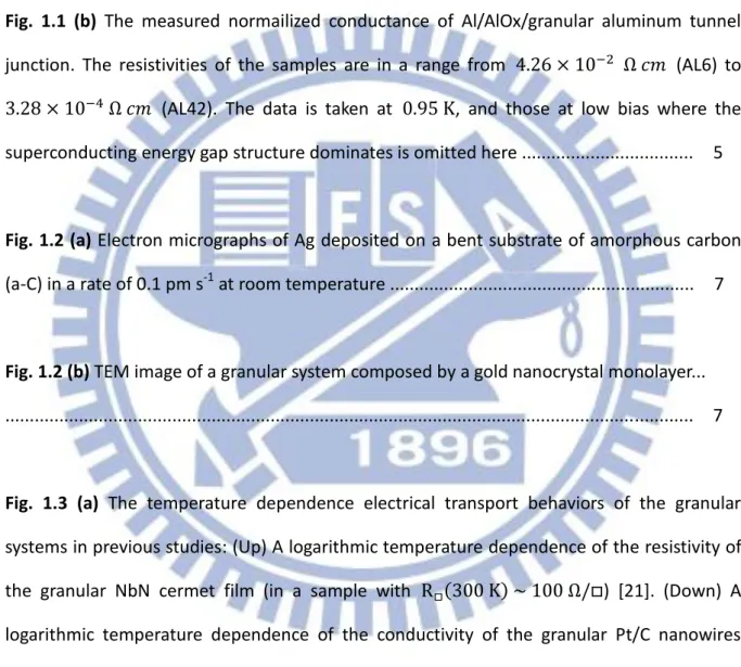
Fig. 1.1 (b) The measured normailized conductance of Al/AlOx/granular aluminum tunnel
junction. The resistivities of the samples are in a range from 4.26 × 10⁻² Ω 𝑐𝑚 (AL6) to 3.28 × 10⁻⁴ Ω 𝑐𝑚 (AL42). The data is taken at 0.95 K, and those at low bias where the
superconducting energy gap structure dominates is omitted here ... 5
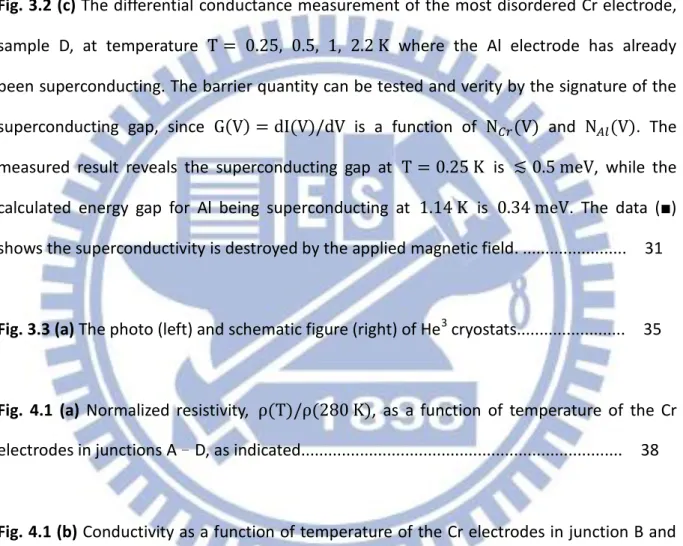
Fig. 1.2 (a) Electron micrographs of Ag deposited on a bent substrate of amorphous carbon
(a-C) in a rate of 0.1 pm s-1 at room temperature ... 7
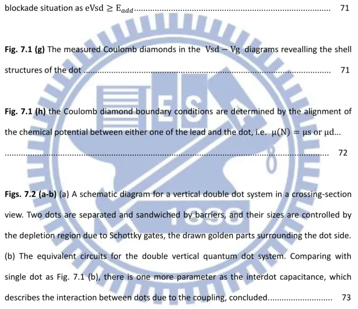
Fig. 1.2 (b) TEM image of a granular system composed by a gold nanocrystal monolayer...
... 7
Fig. 1.3 (a) The temperature dependence electrical transport behaviors of the granular
systems in previous studies: (Up) A logarithmic temperature dependence of the resistivity of the granular NbN cermet film (in a sample with (300 K) ~ 100 Ω/ ) [21]. (Down) A logarithmic temperature dependence of the conductivity of the granular Pt/C nanowires (ρ(300 K) ~ 4 mΩ cm) in a wide range of up to 200 K... 10
Fig. 1.3 (b) Previous,y, the regime g ≪ 1 in the granular has been verified to have the
Efros-Shklovskii type temperature dependence, where the σ ∝ exp(−√T0/𝑇 ) behavior, in
ix
difference between the two curve is the contact resistance. And it was observed in the broad temperature interval of 1 − 100 K, log R is a function of T-1/2... 11
Fig. 2.1 (a) The schematic energy diagram of a metal-insulator-metal (M1-I-M2) tunnel
junction with a finite bias V. ϕ(x) describes the barrier potential. The net tunneling current flow through the junction should be the summation of current from left to right and that from right to left, i.e. I = I12+ I21... 15
Figs. 2.2 (a-b) The schematic energy diagram of a metal-insulator-metal (M1-I-M2) tunnel
junction with (a) zero-bias (b) a finite bias V. Under BDR model, the potential of the barrier 𝜙(𝑥) can be described to be ϕ(x, V) = 𝜙1+𝑥𝑡(𝜙2− 𝑒𝑉 − 𝜙1) (so that ) ϕ(x, 0) = 𝜙1+ 𝑥
𝑡(𝜙2− 𝜙1) for (a) the zero-bias. ... 17
Figs. 3.1 (a-c) Schematic diagrams of the top views (left) and side views (right) of our sample
during the fabrication progresses: (a) The evaporated Al film; (b) Utilizing O2 plasma to
oxidize the surface of the deposited Al film; (c) Depositing Cr film to cross the AlOx/Al structure. The side view shows the junction area where the red dotted lines enclose on the left top view figure... 25
Fig. 3.1 (d) The AFM image of a thin Cr layer, prepared by thermal evaporation deposition on
a mica substrate, shows the granular property. The surface profile below is along the solid line indicated in the AFM image ... 26
Fig. 3.2 (a) Diagrams depicting (up) four-probe resistance measurements of Cr electrodes,
x
strips stand for Al films, and green (gray) strips for Cr electrodes... 29
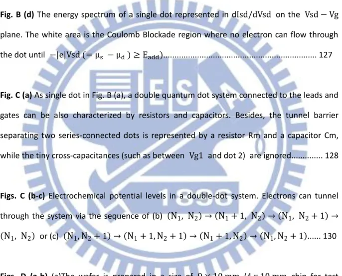
Fig. 3.2 (b) The equivalent circuit for the differential conductance measurements for Cr
electrodes. ... 30
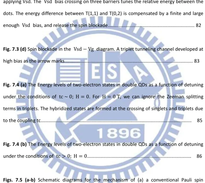
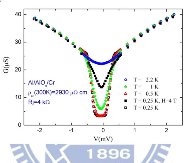
Fig. 3.2 (c) The differential conductance measurement of the most disordered Cr electrode,
sample D, at temperature T = 0.25, 0.5, 1, 2.2 K where the Al electrode has already been superconducting. The barrier quantity can be tested and verity by the signature of the superconducting gap, since G(V) = dI(V)/dV is a function of N𝐶𝑟(V) and N𝐴𝑙(V). The
measured result reveals the superconducting gap at T = 0.25 K is ≲ 0.5 meV, while the calculated energy gap for Al being superconducting at 1.14 K is 0.34 meV. The data (■) shows the superconductivity is destroyed by the applied magnetic field. ... 31
Fig. 3.3 (a) The photo (left) and schematic figure (right) of He3 cryostats... 35
Fig. 4.1 (a) Normalized resistivity, ρ(T)/ρ(280 K), as a function of temperature of the Cr
electrodes in junctions A–D, as indicated... 38
Fig. 4.1 (b) Conductivity as a function of temperature of the Cr electrodes in junction B and
junction D. The straight solid lines are least-squares fits to the equation of conductivity in Sec 2.4... 39
Fig. 4.2 (a) Normalized differential conductance, G(V)/G(70 mV), as a function of bias
voltage for junctions A, C and D, as indicated. Notice that the G(V) curves are essentially symmetric around the zero bias voltage. Data were taken at 2.5 K... 41
xi
Fig. 4.2 (b) The G(V) curve of junction A in zero magnetic field (symbols) and in a
perpendicular magnetic field of 4 T (solid curve). Notice that the magnetic field causes a negligible change. Data were taken at 2.5 K... 42
Fig. 4.2 (c) The G(V) curve of junction D in zero magnetic field (symbols) and in a
perpendicular magnetic field of 4 T (solid curve). Data were taken at 2.5 K... 43
Fig. 4.2 (d) Normalized differential conductance, G(V)/G(10 mV), as a function of bias voltage
for junctions A – D, as indicated. The straight solid lines are least-squares fits to the equation of conductivity in Sec.2.4. For clarity, the data for the junctions B, C and D have been vertically shifted up by 0.1, 0.2 and 0.8, respectively. Data were taken at 2.5 K... 44
Fig. 4.2 (e) G(V)/G(10 mV) versus √V for junctions A, C and D, as indicated. The straight
solid lines are guide to the eyes. Data were taken at 2.5 K... 45
Fig. 4.3 (a) G(V) spectra of junctions A at 2.5 K in a wide bias voltage interval, as indicated.
The symbols are the experimental data and the solid curves are parabolic fits. The solid curves in junctions A are described by Gpara (V ) = 848 + 0.067 V + 0.0028 V2 where
Gpara (V ) is in microsiemens and V in millivolt... 48
Fig. 4.3 (b) G(V) spectra of junctions D at 2.5 K in a wide bias voltage interval, as indicated.
The symbols are the experimental data and the solid curves are parabolic fits. The solid curves in junctions D are described by Gpara = 272 − 0.12V + 0.0026V2, respectively,
where Gpara is in microsiemens and V in millivolt... 49
xii
H = 0 T (triangles) and H = 4 T (squares). The small difference between two curves is within our experimental uncertainty. The results confirm that the WL effect (which is sensitive to the magnetic fields) is irrelevant to our system, while the prediction on conductivity in the theory of granular metals should be valid at any magnetic field... 52
Fig. 4.5 (a) Normalized differential conductance, (G(V, T) − G(0, T) )/√T, as a function of
the combined parameter √eV/k𝐵T for the junction D at five measurement temperatures.
Notice that the data points collapse closely... 55
Fig. 4.5 (b) Unscaled G(V) versus bias voltage V at (from bottom up) 2.5, 5.0, 9.0, 16 and 32
K... 56
Part II
Spin blockade with spin singlet electrons
Fig. 6.2 (a) The schematic diagram of the hyperfine interaction in a double QD system, where
⇑/↑ shows the electron/nuclear spin direction and α is the coupling strength... 64
Fig. 7.1 (a) Schematic diagrams of semiconductor heterostructures such as
AlGaAs/GaAs/AlGaAs that confine electrons to a plane... 67
Figs. 7.1 (b-c) The equivalent circuits for the (b) vertical and (c) lateral quantum dot system.
The gate couples to the dot capacitively, and barriers between electrode reservoirs and the dot can be represented as a parallel connection of resistance and capacitor... 68
xiii
Fig. 7.1 (d) Coulomb Oscillations, the current peaks measured at Vsd ≈ 0. The peaks only
happens when µ(N) = µs = µd, and we can tune µ(N) with Vg. The difference between the two neighboring peaks is the addition energy... 70
Figs. 7.1 (e-f) The schematic diagram for (e) Coulomb oscillation occurring (f) releasing the
blockade situation as eVsd ≥ E𝑎𝑑𝑑... 71
Fig. 7.1 (g) The measured Coulomb diamonds in the Vsd − Vg diagrams revealling the shell
structures of the dot ... 71
Fig. 7.1 (h) the Coulomb diamond boundary conditions are determined by the alignment of
the chemical potential between either one of the lead and the dot, i.e. µ(N) = µs or µd... ... 72
Figs. 7.2 (a-b) (a) A schematic diagram for a vertical double dot system in a crossing-section
view. Two dots are separated and sandwiched by barriers, and their sizes are controlled by the depletion region due to Schottky gates, the drawn golden parts surrounding the dot side. (b) The equivalent circuits for the double vertical quantum dot system. Comparing with single dot as Fig. 7.1 (b), there is one more parameter as the interdot capacitance, which describes the interaction between dots due to the coupling, concluded... 73
Figs. 7.2 (c-d) (c) The charge stability diagram for double quantum dot systems. (d) Three
corresponding level diagram w.r.t the colored circles in Fig. 7.2 (c). Here, we treat two dots as individual ones. Electrons can do the first-order tunneling only at blue point(s)... 74
xiv
coupling between two dots. (g) Diagrams of corresponding chemical potentials of dots and leads at the colored circles in (e). Notice that along the line linking up the paired circles, states in each dot are tuned simultaneously and equally. Unlike Fig. 7.2 (c), the chemical potentials represented as 𝜇1/2(𝑛1, 𝑛2) here are due to the interdot coupling... 76
Fig. 7.2 (h) The Vsd − Vg schematic diagram for the double dot systems. The block lines
sketch the contours of blockade regions. Within the blockade area, red and blue lines show a second-tunneling process. The vertical lines indicate an offset between dots, or the offset number is revealed as the numbers of the vertical line... 77
Fig. 7.2 (i) The measured Vsd − Vg diagram of the double dot systems in dIsd/dVsd plots.
The vertical line indicates an offset = 1 and the corresponding positions of levels are in Fig. 7.2 (j)... 78
Fig. 7.2 (j) The corresponding energy level diagrams for a double dot system with inderdot
offset = 1. At condition a, we can clearly see the energy difference between two dots. Condition b is along the vertical line, while C is at the kink side. For b electrons tunnel through the system via the two aligned ground states at an infinite source-drain bias, The applied gate voltages simultaneously and nearly equally tune states in both dots. Therefore, we have a vertical line, as the tunneling boundary, along the Vg axis... 79
Fig. 7.3 (a) Schematic level diagrams of the Pauli spin blockade: During the
(0,1)(1,1)(0,2)(0,1) cycle, (1,1) has both probability to be either spin singlet or triplets, so the electron may transport until SB will eventually occurs... 81
xv
N=2 as the area green lines enclose. The small current in other red color region is due to the co-tunneling process ... 82
Fig. 7.3 (c) The schematic diagram of the triplet tunneling channel developed by
applying Vsd. The Vsd bias crossing on three barriers tunes the relative energy between the dots. The energy difference between T(1,1) and T(0,2) is compensated by a finite and large enough Vsd bias, and release the spin blockade... 82
Fig. 7.3 (d) Spin blockade in the Vsd − Vg diagram. A triplet tunneling channel developed at
high bias as the arrow marks... 83
Fig. 7.4 (a) The Energy levels of two-electron states in double QDs as a function of detuning
under the conditions of tc ~ 0; H = 0. For H = 0 T, we can ignore the Zeeman splitting terms in triplets. The hybridized states are formed at the crossing of singlets and triplets due to the coupling tc... 85
Fig. 7.4 (b) The Energy levels of two-electron states in double QDs as a function of detuning
under the conditions of tc > 0; H = 0... 86
Figs. 7.5 (a-b) Schematic diagrams for the mechanism of (a) a conventional Pauli spin
blockade and (b) a singlet spin blockade... 87
Fig. 7.6 (a) The Fock-Darwin spectrum describes a single electron within a 2D parabolic
confinement under magnetic fields. At high magnetic field, the Landau levels are formed as marked (n,l)=(0,0),(0,1),(0,2),(0,3)…. Note that the spin degeneracy is ignored here... 89
xvi
Fig. 7.6 (b) The calculated electrochemical potential μ of a two-electron dot as a function of
magnetic field for ℏω0 = 5.6 meV, Ec = 5 meV at 10 T: The lower solid curve is the
ground state (GS), while the upper one is the excited state (ES). Dashed lines represent the situation involving the B-dependent Coulomb interaction. Due to the larger overlap of W.F. when both electrons staying in GS, the dashed line of GS grows faster than that of ES. The upper dashed curve with subtraction of a constant exchange energy results in the dotted curve. The GS, before and after the S-T transition, is indicated by a dashed-dotted line... 90
Fig. 7.6 (c)Plot of Isd(Vg, B) measured in a single QD system with Vsd = 0.1 meV which is so small to show only the ground states (of N = 1 to 5). For N = 2, the ground-state transition is marked with a triangle. The spin configurations, indicated with the arrows, show the transition from spin singlet to be spin triplet as gradually applying the magnetic field from 0 to 4.15 T. Note that the system gains additional exchange energy when the spins of two electrons are parallel ... 92
Fig. 8.1 (a) Schematic energy diagram of a double QD device where only the ground state in
the z-direction occupied. The equilibrium in electrostatic potential among the electrodes and well is reached... 94
Fig. 8.2 (a) A simplified diagram for the wafer structure as in Table 3... 96
Figs. 8.2 (b-f) The main fabricating process in both aerial view and cross-section figures. (b)
The first cross-section figure shows the deposited Ti/Au bottom and top contact. Titanium here is used for bonding metal electrodes and the substrate more tightly. The second and third cross-section figures are steps for the pillar structure. The dry etching process is to “sculpt ” the pillar shape and the following wet etching further lessen semiconductor parts of
xvii
the pillar in width and in depth until beneath the layers of three barrier structures. (c) Evaporating the metal gates around the pillar. (d-f) are steps for the contact pads for wire bonding. In (d), we use wet etching beneath the semi-insulating substrate; (e) step smoother with hard bake resist; (f) evaporating the metal contacts... 97
Figs. 8.2 (g-j) Photos of device similar with our samples. (g) A SEM image of a double-gate
vertical QD device. (h) A image under optical microscope; two devices are included. (i) Contact pads for wire bonding. (j) A sample wire bonding to a chip carrier... 98
Figs. 8.3 (a-b) (a) Copper powder filters, which can work well as a low pass filter even at low
temperatures, are launched between the sample holder and mixing chamber of the fridge (b) The structure of the copper powder filter... 100
Fig. 9.1 (a) dIsd/dVsd plots under magnetic field from 0 to 5 T. The Spin blockade region is
indicated by the dotted line at 0 T. The triplet channel which collapses the spin blockade is marked by arrows. With increasing the magnetic field, the triplet channel enters into the SB region and approaches to the zero bias, but the CB is still left ... 102
Fig. 9.1 (b) The Vsd − Vg diagrams measured at 0 T with different gate conditions. The
upper diagram shows the offset=1 case where µ1(1,1) = µ2(0,2), whereas µ1(1,1) >
µ2(0,2) at the underlying diagram. These two diagrams demonstrate the ability to detune
the interdot offset in our device... 103
Fig. 9.2 (a) The Coulomb diamond diagram at 0 T. To measure the two-electron state energy
spectrum, we sweep gate voltages along the yellow arrow to trace the variation of chemical potential of (0,2) states from 0 to 10 T, and the result is shown in Fig. 9.2 (b). The yellow
xviii
line indicated µ2(0,2) is the ground (0,2) state before the S-T transition... 104
Fig. 9.2 (b) The excitation energy spectrum for (0,2) states, measured at Vsd = − 4 mV. The
first current strip exhibits the (0,2) state evolution among the solid line of the 1s2 orbital (0,2) state with spin singlet, the dashed line of the 1s2p+ orbital (0,2) state with spin triplet, and the dotted line for another (0,2) state with spin singlet... 105
Figs. 9.3 (a-b) dIsd/dVsd plots under the magnetic fields of (a) 0.0 T, (b) 2.0 T. The
arrows mark the threshold of SB... 108
Figs. 9.3 (c-d) dIsd/dVsd plots under the magnetic fields of (c) 4.0 T, (d) 5.0 T. The arrow
marks the threshold of SB. At 5.0 T, SB is completely relieved and only the Coulomb blockade region is left... 109
Figs. 9.3 (e-f) dIsd/dVsd plots under the magnetic fields of (e) 6.2 T, (f) 7.4 T. The arrow s
mark the threshold of SSB... 110
Fig. 9.3 (g) Plots of the energy difference between the ground and 1st excited (0,2) states, ΔEge. Circles indicate data extracted from (0,2) excitation spectrum in Fig. 9.2 (b), and triangles are data from the series of Coulomb diamond measurements shown in Figs. 9.3 (a-f). ΔEge measured as VgL/Vg (Fig. 9.2 (b)) and Vsd (Figs. 9.3 (a-f)) are converted to
energy using the voltage drop ratio of three tunneling barriers. ... 111
Fig. 9.4 (a) The Isd − Vsd curve along the dashed line in the insert Vsd − Vg diagram
xix
Fig. A (a) The schematic diagram of the electron/nuclear spins, represented as ⇑/↑, in a
imaged system that there are only two nuclear spins in each dot. Under SSB, the system is blocked with electron spin singlet until it interacts with nuclear spins via the hyperfine interaction and release the SSB by spin flip-flop process which passes the entanglement to the nuclear pairs. The α indicates the hyperfine interaction strength (see Sec. 6.2)... 116
Fig. A (b) The diagram that the nuclear spins change among mix2 𝑆 ∙ 𝑚𝑖𝑥, and 𝑆2 condition. The arrow show the change of the direction and the number above is the change probability... 119
Fig. A (c) Assuming there are N nuclear spins in both QD1 and QD2, then after nth hyperfine
interaction to exchange the spin state with electron spin singlet under SSB, the nuclear spins have mix𝑁, Smix𝑁−1, S2mix𝑁−2, … or S𝑁possible conditions... 121
Fig. A (d) The diagram of the nuclear spins changing among the mix𝑁, Smix𝑁−1, S2mix𝑁−2, … or S𝑁 possible conditions. Whenever the interaction acts at
the condition of S𝑛mix𝑚 (n + m = N), it may change to be S𝑛+1mix𝑚−1, S𝑛mix𝑚 or S𝑛−1mix𝑚+1. The arrow show the change of the direction and the number above is the
probability... 121
Fig. B (a) An equivalent circuit for the single-quantum-dot system. The dot connected to the
leads via tunnel barriers is characterized by parallel series of the resistor Rs/Rd and the capacitor Cs/Cd, while it capacitively couples to the gate through a capacitor Cg... 124
xx
flow via the system only when levels falls within the bias window determined by µs and
µd... 125
Fig. B (c) The schematic diagram for a Coulomb diamond. The alignment between 𝜇(𝑁) and
at least one of µlead determines the boundaries. ... 126
Fig. B (d) The energy spectrum of a single dot represented in dIsd/dVsd on the Vsd − Vg
plane. The white area is the Coulomb Blockade region where no electron can flow through the dot until −|e|Vsd (= µs − µd ) ≥ Eadd)... 127
Fig. C (a) As single dot in Fig. B (a), a double quantum dot system connected to the leads and
gates can be also characterized by resistors and capacitors. Besides, the tunnel barrier separating two series-connected dots is represented by a resistor Rm and a capacitor Cm, while the tiny cross-capacitances (such as between Vg1 and dot 2) are ignored... 128
Figs. C (b-c) Electrochemical potential levels in a double-dot system. Electrons can tunnel
through the system via the sequence of (b) (N1, N2) → (N1+ 1, N2) → (N1, N2+ 1) → (N1, N2) or (c) (N1,N2+ 1) → (N1+ 1,N2+ 1) → (N1+ 1,N2) → (N1,N2+ 1)... 130
Figs. D (a-b) (a)The wafer is prepared in a size of 9 × 10 mm (4 x 10 mm chip for test
samples) for the following fabrication processes (b) The simplified schematic diagram of the water structure composed of multilayers as Table 3... 131
Fig. D (c) Schematic diagrams of the top views (left) and the side views (right) of the wafer
xxi
Fig. D (d) Schematic diagrams of the top views (left) and the side views (right) of the wafer
during the top contact fabrication... 133
Fig. D (e) Schematic diagrams of the top views (left) and the side views (right) of the wafer
during the dry etch process... 134
Fig. D (f) Schematic diagrams of the top views (left) and the side views (right) of the wafer
during the wet etch process... 135
Fig. D (g) Schematic diagrams of the top views (left) and the side views (right) of the wafer
during the gate fabrication... 136
Fig. D (h) Schematic diagrams of the top views (left) and the side views (right) of the wafer
during the mesa process. ... 138
Fig. D (i) Schematic diagrams of the top views (left) and the side views (right) of the wafer
during the step smoother process... 140
Fig. D (j) Schematic diagrams of the top views (left) and the side views (right) of the wafer
- 1 -
Part I
Conductivity and tunneling density of states
in granular Cr films
- 2 -
Chapter 1
Introduction
1.1 A Puzzle in Chromium Systems
A half century ago, Rowell and Shen [1] observed a zero-bias anomaly (a “resistance peak”) in Cr/CrOx/Ag tunnel junctions comparatively much larger than the junctions composed by other materials (see Fig. 1.1 (a)). Then subsequently, such a giant zero-bias anomaly has also been found in experiments involving Cr as the electrodes by other groups [2-4]. Rowell and Shen attributed this giant resistance peak (conductance dip) in their Cr/CrOx/Ag junctions to the magnetic nature of the insulating barrier, while CrO2 is
antiferromagnetic and Cr2O3 is ferromagnetic. On the other hand, Mezei and Zawadowski [5]
suggested that the effect is owing to the Kondo scattering from magnetic moments embedded in the Cr electrode or at the electro-insulator interface. However, the main difficulty with the explanation is that the magnitude of the anomaly was not satisfactory with that stemming from the effect. Thus far, what really accounting for the great zero-bias resistance peaks found in many Cr consisted tunnel junctions has remained mysterious.
On one hand, the Chromium system is antiferromagnetic and its oxide, CrOx, possess magnetic nature, while, on the other hand, it often forms a granular-like structure [6-8] if it is thermally deposited. The forming of granules brings the disorder to the system. Altshuler
- 3 -
and coworkers [9-13] have studied the EEI effect in the presence of weak disorder. They found that the EEI effect causes to a suppression in the electron DOS at the Fermi level. And, it is also predicted that in the weakly disordered regime the density of states (DOS), proportional to the junction conductance, have the dependence on the voltage (energy). Meanwhile, McMillan [14, 15] proposed that the correlation on the DOS of a 3-dimentional (3D) system on metallic side near the Metal-Insulation transition systems is in the form which is similar to the expression given by Altshuler and Aronov [13]:
for E < ∆, N(E) = N(0)[1 + (E/∆)1/2]
where N(0) is the DOS at the Fermi energy level EF, and Δ, called “correlation gap”, is
a characteristic energy scale that vanishes as a power of the distance to the metal-insulator transition (for a system crossing over from the metallic side to be the insulator, the correlation gap gradually decreases to zero at the Metal-Insulation transition, and raise again). And, the comparison between this theory and the experiment results on Al/AlOx/granular Al tunnel junction is also made in Ref. [16] (see Fig. 1.1 (b)).
While the puzzle in tunnel junction of the Cr electrode (with the granular property) has not been answered, the theory on granular system is proposed in recently years. Therefore, before analyzing the role the granular property may play in Cr system, we start from giving a briefly introduction on the relative theory in next section.
- 4 -
(a)
Fig. 1.1 (a) Conductances versus voltage plot of several normal metal junction exhibiting different zero-bias behaviors. The Data were taken at 1 K [17].
- 5 -
(b)
Fig. 1.1 (b) The measured normailized conductance of Al/AlOx/granular aluminum tunnel junction. The resistivities of the samples are in a range from 4.26 × 10⁻² Ω 𝑐𝑚 (AL6) to 3.28 × 10⁻⁴ Ω 𝑐𝑚 (AL42). The data is taken at 0.95 K, and those at low bias where the
- 6 -
1.2 The Introduction on Granular Conductors
The granular conductor here is considered a system with metallic grains embedded in dielectric components. The size of the grain is from a few to hundreds of nm, therefore the metallic grain is often regarded as an artificial atom with the discrete energy spectrum. On the other hand, the tunablity of the electric properties of the whole system via the size of the grain, the tunneling coupling between grains, and so on also make the granular conductor treated as an artificial solid. The mean energy level spacing in a single granule (depending on the granular size), δ, the dimensionless tunneling conductance between neighboring granules (i.e. the tunneling coupling), g, and the single-grain Coulomb charging energy, Ec characterize granular material. These parameters are relative to the disorder effect, the quantum confinement, and the electron correlation. The interplay among those effects with tunable parameters we can control brings the attention to the granular conductors.
There are several ways to fabricate the granular system. Traditionally, the granular conductor can be made by sputtering or the thermal evaporation (see Fig. 1.2 (a)). Depending on the material such as chromium in our system, as it deposits on the substrate, it naturally gather to form the granular structure. However, the size of grains is not uniformed. The dielectric component is formed during the evaporation as the surface is oxidized. In some systems, the tunneling coupling between grains is determined and adjusted by covering the organic or inorganic molecules on grains [18]. The other ways to have granular system are, for example, with the self-assembling colloidal nanocrystals or the self-assemble semiconductor quantum dot [19]. The variation of particles in size can be controlled to be within less than with the thermal evaporation method as the gold nanocrystal colloid in Fig. 1.2 (b) [18]. The relative standard deviation of the size is about 5%. As for the self-assemble semiconductor quantum dot, it is utilized the different lattice constant of two
- 7 -
semiconductors.
(a)
Fig. 1.2 (a) Electron micrographs of Ag deposited on a bent substrate of amorphous carbon (a-C) in a rate of 0.1 pm s-1 at room temperature [20].
(b)
Fig. 1.2 (b) TEM image of a granular system composed by a gold nanocrystal monolayer [18].
- 8 -
1.3 Why We Study Granular Cr films?
In this thesis, we study four the Al/AlOx/Cr planar tunnel junctions comprising of granular Cr electrodes. The non-magnetic insulating barrier AlOx was intentionally used, instead of the magnetic CrOx, to rule out the possible influence of the magnetic nature of barrier on the tunneling signals. Besides, the attempt to answer the puzzle in history, we also have a great interest in the granular conductors.
Experimentally, it is intriguing that electrical-transport measurements on granular systems with strong intergrain coupling often revealed ln T dependence of resistivity [21, 22], rather than of conductivity [23, 24] as the theory predicted (see Sec.2.4 and Fig. 1.3 (a)). Therefore, it still awaits convincing experimental test. Moreover, to the best of our knowledge, there is still no experimental observation in three-dimensional (3D) granular films concerning the electronic DOS. Thus, we are motived to study Al/AlOx/granular Cr tunnel junctions. The dimensionality of the granular arrays (the Cr electrodes) was made to have d = 3, and both conductivities and tunneling DOS of the Cr electrodes (with intergrain tunneling conductance spanning from g ≅ 1 to g ≫ 1) are measured to verified the recent theory of granular metals [25-27]. We would like to mention that previously in our experiment, we found a Efros-Shklovskii type temperature dependence in the nanocontacts formed with granular Cr films, where the σ ∝ exp(−√T0/T ) behavior was observed in the
broad temperature interval of 1 − 100 K [6] (see Fig. 1.3 (b)), while the conductivity at low temperatures is theoretically established to possess this type-like dependence in the opposite limit of weak intergrain coupling (g ≪ 1), for T0 is a characteristic temperature
[23,28-31]. In that case, we experimentally realized the regime g ≪ 1 [32].
This thesis is organized as follows: In Chap. 2, besides the granular system, the the EEI effects and the property of tunnel junctions are also briefly introduced. We discuss our experimental considerations, methods and setups in Chap. 3. Chapter 4 contains our
- 9 -
experimental results and discussions. We interpret our measured conductivity and tunneling DOS in terms of the theory of granular metals, and rule out the WL and EEI effects developed for weakly disordered homogeneous conductors to be the origins of our observations. Finally, our conclusion is presented in Chap. 5.
- 10 -
(a)
Fig. 1.3 (a) The temperature dependence electrical transport behaviors of the granular systems in previous studies: (Up) A logarithmic temperature dependence of the resistivity of the granular NbN cermet film (in a sample with (300 K) ~ 100 Ω/ ) [21]. (Down) A logarithmic temperature dependence of the conductivity of the granular Pt/C nanowires (ρ(300 K) ~ 4 mΩ cm) in a wide range of up to 200 K [24].
- 11 -
(b)
Fig. 1.3 (b) Previous,y, the regime g ≪ 1 in the granular has been verified to have the Efros-Shklovskii type temperature dependence, where the σ ∝ exp(−√T0/𝑇 ) behavior,
in our experiment. In this experiment, the nanocontacts formed with granular Cr films, and the difference between the two curve is the contact resistance. And it was observed in the broad temperature interval of 1 − 100 K, log R is a function of T-1/2 [5].
- 12 -
Chapter 2
Background and Theory
There are three main parts will be introduced in this chapter. In this thesis, we measure the differential conductance to investigate the DOSs of the granular Cr electrode, so we start with Sec. 2.1 the general tunneling behavior in metal-insulator-metal junctions and Sec. 2.2
the BDR Model describes the background tunneling conductance in the junctions. Then
from Sec. 2.3 to 2.4, theoretical predictions related to our system will be introduced. Since the granular conductor is also a disorder system, the electron-electron interaction (EEI) effects, which have well explained weak disorder systems, will be mentioned in Sec.2.3. And finally, the theoretical prediction for the granular electronic system is in Sec. 2.4.
2.1 Tunneling in Metal-Insulator-Metal Tunnel Junctions
In this thesis, we measure the tunneling current through the metal-insulator –metal (M-I-M) tunnel junctions to investigate the DOS of granular conductors. In order to know the relation between the DOS of electrodes and the tunneling current, we start with the basis of the tunneling mechanism and extend to obtain the tunneling current in such a junction structure. Then, the relation of the DOS of electrodes and the differential conductance will be derived.
- 13 -
with a potential higher than its total energy. However, in quantum mechanism, whenever a particle treated as a wave runs into a barrier potential, there will be both probabilities to penetrate it and to be reflected. In our cases, we can consider the energy diagram in a M-I-M tunnel junction similar toFig. 2.1 (a): x < 0 (the left of the barrier), 0 < x < t (within the barrier), t < x (the right of the barrier). The wave incident from the left is expressed to be e𝑖𝑘𝑥 for k =√2𝑚𝐸
𝑥/ℏ (𝐸𝑥: total energy of the tunneling particle in the x direction, m: the
effective mass) and it decays in an exponential form, e−𝜅𝑥 for κ = √2𝑚(𝜙(𝑥) − 𝐸𝑥)
(𝜙(𝑥): the barrier potential), inside the barrier. And, the wave penetrated to the right is Te𝑖𝑞𝑥. The transmission coefficient, D, is a ratio of the probability flux transmitted through
the barrier to the probability flux incident upon the barrier. For an extremely small transmission [33], D can be reduced to be
D(E𝑥) = ge−2𝐾,
where g =(𝑘2+𝜘16𝑘𝑞𝜘2)(𝑞22+𝜘2) and K =∫ 𝜘(𝑥, 𝐸0𝑡 𝑥)𝑑𝑥. Notice that D is a function of both
barrier height and thickness.
If we apply a voltage on this M-I-M junction, the Fermi levels of the two electrodes originally aligned will be shifted. The chemical potential in Metal 2 is lowered by eV by considering the schematic circuit in Fig. 2.1 (a). For eV >> k𝐵T, the current density flow
from Metal 1 to Metal 2 can be expressed as [33]
𝐽1,2(V) = − 2e (2𝜋)3 ∫ ∫ ∫ 𝑑𝑘𝑥𝑑𝑘𝑦𝑑𝑘𝑧𝑣𝑥𝐷(𝐸𝑥, 𝑉) 𝑘𝑧 𝑘𝑦 𝑘𝑥 𝑓(𝐸)(1 − 𝑓(𝐸 + 𝑒𝑉)) = −(2𝜋)2e3ℏ∫ ∫ ∫ 𝑑𝐸𝐸𝑥 𝑘𝑦 𝑘𝑧 𝑥𝑑𝑘𝑦𝑑𝑘𝑧𝐷(𝐸𝑥, 𝑉)𝑓(𝐸)(1 − 𝑓(𝐸 + 𝑒𝑉)) for 𝑣𝑥 = 1ℏ𝑑𝑘𝑑𝐸 𝑥
- 14 -
where 𝑓 is the Fermi-Dirac distribution for 𝑓1 = 1 1+𝑒 𝐸−𝜇1 k𝐵T = 𝑓(𝐸) and 𝑓2 = 1 1+𝑒 𝐸−(𝜇1−𝑒𝑉) k𝐵T
= 𝑓(𝐸 + 𝑒𝑉). 𝑘𝑦 and 𝑘𝑧 are symmetric, and we express 𝑑𝑘(2𝜋)𝑦𝑑𝑘2𝑧 = 𝜌𝑟𝑑𝐸𝑟 for
𝜌𝑟 and 𝐸𝑟 are the DOSs and the energy in the y-z plane. Therefore,
𝐽1,2(V) = −2e𝜌𝑡
ℎ ∫ ∫ 𝑑𝐸𝐸𝑥 𝐸𝑟 𝑥𝑑𝐸𝑟𝐷(𝐸𝑥, 𝑉)𝑓(𝐸)(1 − 𝑓(𝐸 + 𝑒𝑉)),
Similarly, from Metal 2 to Metal 1, 𝐽2,1(V) = − 2e𝜌𝑡 ℎ ∫ ∫ 𝑑𝐸𝑥𝑑𝐸𝑟𝐷(𝐸𝑥, 𝑉) 𝐸𝑟 𝐸𝑥 𝑓(𝐸 − 𝑒𝑉)(1 − 𝑓(𝐸)) Then, the net current density would be
𝐽 = 𝐽2,1(V) − 𝐽1,2(V) = −2e𝜌𝑡 ℎ ∫ ∫ 𝑑𝐸𝑥𝑑𝐸𝑟𝐷(𝐸𝑥, 𝑉) 𝐸𝑟 𝐸𝑥 [𝑓(𝐸) − 𝑓(𝐸 + 𝑒𝑉)]
For T ⟶ 0 K, all electron stay below the Fermi energy, hence, the tunnel only involve the electrons of energy within the transport window opened by eV, so
𝐽 = −2e𝜌𝑡
ℎ ∫ ∫ 𝑑𝐸𝑥𝑑𝐸𝑟𝐷(𝐸𝑥, 𝑉)
𝐸𝑟 𝐸𝑥
- 15 -
(a)
Fig. 2.1 (a) The schematic energy diagram of a metal-insulator-metal (M1-I-M2) tunnel
junction with a finite bias V. ϕ(x) describes the barrier potential. The net tunneling current flow through the junction should be the summation of current from left to right and that from right to left, i.e. I = I12+ I21.
- 16 -
2.2 The BDR Model
-- the Background Tunneling Conductance in the Metal-Insulator-Metal Tunnel Junction
Figure 2.2 (a) shows the schematic energy diagram in a metal-insulator-metal tunnel junction. As such a structure is made, the Fermi energies of two metals become equal after the system reaches the equilibrium, and the barrier is asymmetric due to the different work function in the metals. That is, the barrier height seen from two electrodes is different, i.e. ϕ1 for Metal 1 and ϕ2 for Metal 2 as showed.
In order to see how the voltage bias affects the tunneling behavior in this tunnel junction, Brinkaman, Dynes and Rowell [34] (BDR model) describe the asymmetric barrier height in a simple form (corresponding to Fig. 2.2 (b)):
ϕ(x, V) = 𝜙1+
𝑥
𝑡(𝜙2− 𝑒𝑉 − 𝜙1)
where t is the barrier thickness. And, we can calculate the differential conductance G(V) =𝜕𝐽(𝑉)𝜕 𝑉 by integrating 𝐷(𝐸𝑥, 𝑉) with ϕ(x, V) to have (V). At the low bias,
G(V) = G(0)[1 − (𝐴0∆𝜙 16𝜙̅32
) eV + (9𝐴0
2
128𝜙̅)(eV)2]
for G(0), the zero-bias conductce, 𝐴0 =4(2𝑚) 1/2𝑡
3ℏ , Δϕ = 𝜙2 − 𝜙1 and 𝜙̅ = 𝜙1+𝜙2
2 . The
G(V) depands on the bias approximately in a parabolic form under the BDR model, and we notice that the minimum value takes place at the zero bias for Δϕ = 0 or when the barrier is symmetric.
- 17 -
(a)
(b)
Figs. 2.2 (a-b) The schematic energy diagram of a metal-insulator-metal (M1-I-M2) tunnel
junction with (a) zero-bias (b) a finite bias V. Under BDR model, the potential of the barrier 𝜙(𝑥) can be described to be ϕ(x, V) = 𝜙1+𝑥𝑡(𝜙2− 𝑒𝑉 − 𝜙1) (so that ) ϕ(x, 0) =
- 18 -
2.3 The Electron-Electron Interaction in Disorder System
The electron-electron interaction (EEI) and weak localization effects in disordered systems have been studied for decades [9-13, 35]. Although both the two effects contribute significantly to the electrical conduction properties of a given system, it is possible to understand the individual contribution. Indeed, the EEI effect can be isolated by studying the differential conductances, G(V, T) = dI(V, T)/dV , of a metal-insulator-metal tunnel junction at low temperatures. Here the (left) reference electrode is made of a clean metal while the (right) electrode is often made of a weakly disordered metal to be investigated.
According to Altshuler and coworkers [9-13], the EEI effect in the presence of weak disorder will lead to suppression in the electron density of states (DOS) near the Fermi level. Moreover, such a DOS singularity is predicted to be sensitive to both bias voltage and temperature. At a low temperature (to ignore the thermal smearing effect), and at the weak-disorder limit, i.e.,k ≫ 1, where k is the Fermi wavenumber and is the elastic mean free path of electrons, the EEI-induced correction to the DOS, δNd(E), depends strongly on the effective dimensionality d of the sample and has the following forms:
for d = 2, the correction is given by [9, 11, 12]
δN
2(E)
N
2(0)
=
λ
2e
28π
2ℏ
𝑅
ln [
E
ℏD
(
t
2π
)
2]
where λ2 depends on the form of the effective EEI and for long range Coulomb
interactions [5]
λ
2= ln [
ℏDκ24t2 (2π)2E]
- 19 -
with
κ
2=
me2k 𝐹 t
2𝜋2ℏ2𝜖0, where 𝜖0 is the permittivity of the vacuum.
for d = 3, the correction is given by [5, 13]
δN
3(E)
N
3(0)
=
λ
3√𝐸4√2𝜋
2(ℏ𝐷)
3/2N
3
(0)
Here N2(0) and N3(0) are the DOS at Fermi level in the d = 2 and d = 3 case
respectively, is the sheet resistance, D is the diffusion constant, t is the film thickness, and τ is the electron momentum relaxation time. The electron energy E is measured relative to the Fermi energy. Besides, the theory predicts that a crossover from two to three dimensions should occur at a characteristic bias energy eVc = Ec ≈ (2π)2(ℏD/t2). This critical energy corresponds to an EEI characteristic length of Lc =√ℏD/Ec ≈ t/2π. Notice that the characteristic bias voltage Vc scales with D/t2, and hence it reduces with increasing disorder.
For a metal-insulator-metal tunnel junction comprised of a clean metal and a disordered metal, at low temperatures, the variation in the differential conductance G(V) directly reflects the energy dependence of DOS of the disordered metal [33]: G(V) = PN𝑐(0)N𝑑(eV), where P is the tunneling rate which depends on the barrier
properties (barrier height and thickness), N𝑐 is the DOS of the clean metal which depends
weakly on energy and can be approximated as the value at Fermi level N𝑐(0), and N𝑑 is the
DOS of the disordered metal. Thus, the normalized conductance G(V)/G(0) = N𝑑(eV)/
N𝑑(0) can be compared with
δN2(E) N2(0) and
δN3(E)
N3(0) to study the DOS suppression in
disordered metals quantitatively. In particular, G(V) obeys a lnV law in two dimensions, while it obeys a √V law in three dimensions.
- 20 -
junctions, the DOS singularities have been investigated by several groups. Both weakly [36-41] and strongly [15, 16, 42] disordered metal electrodes have been employed. In recent years, the EEI theory has further been critically tested by high-resolution photoemission spectroscopy measurements [43]. In general, it is found that the EEI theory is fairly successful in explaining the experimentally observed DOS singularities in weakly disordered conductors. In addition, the EEI prediction of a crossover from the two-dimensional G(V) ∝ lnV law [11, 12] to the three-dimensional G(V) ∝ √V law [13] as the bias voltage increases has been confirmed by several experiments [36-39, 41] where electrodes of metal films in the tunnel junctions were used.
2.4 Theoretical Prediction for Granular Electronic Systems
Granular conductors, which are composite materials of metallic granules and dielectric components, have recently attracted much renewed theoretical attention as tunable systems for addressing mesoscopic physics problems [25, 26]. In contrast to disordered “homogeneous systems”, the electronic transport properties of granular conductors are largely governed by the strength of the intergrain tunneling [25]. Theoretically, a granular conductor is characterized by a number of physical quantities: the mean energy level spacing in a single granule, δ, the dimensionless tunneling conductance between neighboring granules, g (i.e., the average tunneling conductance between neighboring grains expressed in units of 2e2/h), and the single-grain Coulomb charging energy, Ec. For strong intergrain coupling (g ≫ 1) and in the not-too-low temperature interval g ≪ k𝐵T ≪ Ec (where k𝐵
is the Boltzmann constant), charging effects are important yet the quantum-interference weak-localization (WL) effects are suppressed. This unique regime provides a tempting
- 21 -
opportunity to probe the electronic conduction properties due to the many-body Coulomb interaction effects in the presence of granularity. The electrical conductivity σ is predicted to obey the law [26, 44]
σ(T) = σ(0)[1 −
2𝜋𝑔𝑑1ln (
𝑘𝑔𝐸𝑐𝐵𝑇
)]
where d is the dimensionality of the granular array, and σ(0) = 2(e2/h)ga2−𝑑 is the classical conductivity without the Coulomb interaction (i.e., the system conductivity at temperature k𝐵T ≫ Ec), and a is the radius of the (spherical) grain. It is important to
note that, unlike that due to the WL and electron-electron interaction (EEI) effects in weakly disordered homogeneous systems [9], this σ ∝ ln 𝑇 law is predicted to hold for all dimensions, since the dimensionality d only enters the prefactor of the logarithmic correction term. On contrary, the functional form of the tunneling electronic density of states (DOS) is predicted to depend critically on sample dimensionality:
for d = 3 [26, 44],
ν
3(ϵ) = ν
0[1 −
A4𝜋𝑔
ln (
𝑔𝐸𝑐
max(𝑘𝐵𝑇,𝜖)
)]
where ϵ is the tunneling electron energy measured from the Fermi energy level (EF),
𝜈0 is the DOS in the absence of Coulomb interaction, and A is a numerical prefactor;
for d = 2
ν
2(ϵ) = ν
0exp[−
1
16𝜋
2𝑔
ln
2(
𝑔𝐸𝑐
- 22 -
The underlying physics which leads to the conductivity and DOS corrections is due to the presence of local voltage fluctuations between neighboring granules.
- 23 -
Chapter 3
Experimental Method
3.1 Sample Fabrication
To study the conductivity and the tunneling DOS of granular Cr films, we fabricated four Al/AlOx/Cr planar tunnel junctions by using the standard thermal evaporation method:
1. First, a set of parallel, relatively clean 0.8 or 1 mm wide and 25 nm thick Al films were deposited on glass substrates held at room temperature.
2. Then, surfaces of the as-deposited Al films were subsequently oxidized by utilizing plasma discharge to produce a ≈ 1.5– 2 nm − thick AlOx layer.
3. Finally, a long Cr electrode (1 mm wide, and 15– 30 nm thick) was then deposited across the parallel AlOx coated Al strips to complete the tunnel junction geometries. At the same time, the Cr electrode was attached with leads appropriate for four-probe electrical measurements.
- 24 -
above. The resistivities of our Al reference electrodes were typically 13 (16) µΩ cm at 4 (300) K, corresponding to the product k ≈ 54 at 4 K, where k is the Fermi wavenumber and is the electron mean free path. The conductivity of the Cr electrode in each set of junctions was adjusted by varying the mean Cr film thickness and the deposition rate between 0.01 and 1.5 nm/s. To achieve a very low conductivity in the junction D, the Cr film was deposited onto a cold substrate held at liquid-nitrogen temperature, by employing a very low deposition rate of ∼ 0.01 nm/s.
The reason for selecting Cr as our electrode is because Cr films deposited in a vacuum often form granular, rather than uniform and continuous, layers [6-8]. For example, a 10 − nm − thick Cr film deposited by thermal evaporation on a mica substrate showed a distribution of disk-shaped granules with a diameter of ~ a few tens of nanometer and a height of ≈ 2– 6 nm, as was evidenced from atomic force microscopy (AFM) studies (see Fig. 3.1 (d) [6]). Varying the deposition rate modified the average grain size [6]. Even thermally evaporated in a vacuum having a background pressure as low as ∼ 1 × 10⁻⁶ mbar, the surfaces of Cr granules became oxidized and formed thin dielectric layers of CrOx [8]. In this work, we carried out our thermal evaporation deposition at a pressure of ∼ 5 × 10⁻⁶ mbar so that our films were guaranteed to form metallic Cr granules separated by thin CrOx dielectric layers. Table 1 lists the values for the relevant parameters of the four Cr electrodes comprising the tunnel junctions A–Dstudied in this work.
- 25 -
(a)
(b)
(c)
Figs. 3.1 (a-c) Schematic diagrams of the top views (left) and side views (right) of our sample during the fabrication progresses: (a) The evaporated Al film; (b) Utilizing O2 plasma to
oxidize the surface of the deposited Al film; (c) Depositing Cr film to cross the AlOx/Al structure. The side view shows the junction area where the red dotted lines enclose on the left top view figure.
- 26 -
(d)
Fig. 3.1 (d) The AFM image of a thin Cr layer, prepared by thermal evaporation deposition on a mica substrate, shows the granular property. The surface profile below is along the solid line indicated in the AFM image [6].
- 27 -
Table 1 Values for relevant parameters of the Cr electrodes in Al/AlOx/Cr tunnel junctions.
is the junction area and is the junction resistance at 300 K. t is the thickness, ρ ( ) is the resistivity (sheet resistance) at 2.5 K, and N𝑐𝑟,𝑑(0) is the DOS at the Fermi energy. k
was calculated by using the Drude model. The diffusion constant D was evaluated through the Einstein relation ρ−1 = N𝑐𝑟,𝑑(0)𝑒2D. The values of k ℓ and D were evaluated for
2.5 K. Ec, σ0, g and a are defined in Sec. 2.4. Notice that the values of a are only listed for
reference, because our Cr granules are disk-shaped rather than spherical.
Sample 𝐍𝒄𝒓,𝒅(𝟎) (mm2) (kΩ) (nm) (µΩ − cm) (Ω) ( −1 m−3) A 0.8 × 1.0 1.0 30 115 38.3 2.4 × 1047 B 0.8 × 1.0 4.5 25 154 61.6 1.8 × 1047 C 1.0 × 1.0 11 15 290 193 1.1 × 1047 D 0.8 × 1.0 4.0 25 5060 2024 2.8 × 1046 Sample 𝟎 (cm2/s) (meV) (Ω−1 cm−1) (nm) A 5.1 1.4 5 8690 62 5.5 B 4.1 1.4 7 6560 42 5.0 C 2.6 1.3 4 3500 10 2.2 D 0.23 0.28 22 260 0.96 2.8
- 28 -
3.2 Experimental Methods
In our experiments, we measured the resistivity of Cr films with the four-probe method, while the tunneling differential conductances, G(V, T) = dI(V, T)/dV, across the junctions were measured by utilizing the standard lock-in technique, where I is the tunneling current between the Al and Cr electrodes, and V is the voltage dropped across the insulating barrier (see Fig. 3.2 (a) for a schematic diagram). Figure 3.2 (b) shows the equivalent circuit of measuring the differential conductance to have the DOS of Cr (see Sec. 2.1).
To ensure the quality of each tunnel junction, we measured the superconducting gap of the clean Al electrode at 0.25 K before performing detailed measurements of G(V, T) curves. Our Al electrodes became superconducting at ≈ 1.8 – 2 K, and Fig. 3.2 (c) shows one of the results in Sample D. Due to the great change of the superconducting gap in the differential conductance, the experiment, different from measurement for the G(V) = dI(V)/dV of Cr electrodes, is performed by applying V to measure I. The equivalent circuit is in Fig. 3.2 (d).
- 29 -
(a)
Fig. 3.2 (a) Diagrams depicting (up) four-probe resistance measurements of Cr electrodes, and (down) differential conductance measurements of Al/AlOx/Cr tunnel junctions. Black strips stand for Al films, and green (gray) strips for Cr electrodes.
- 30 -
(b)
Fig. 3.2 (b) The equivalent circuit for the differential conductance measurements for Cr electrodes.
- 31 -
(c)
Fig. 3.2 (c) The differential conductance measurement of the most disordered Cr electrode, sample D, at temperature T = 0.25, 0.5, 1, 2.2 K where the Al electrode has already been superconducting. The barrier quantity can be tested and verity by the signature of the superconducting gap, since G(V) = dI(V)/dV is a function of N𝐶𝑟(V) and N𝐴𝑙(V).
The measured result reveals the superconducting gap at T = 0.25 K is ≲ 0.5 meV, while the calculated energy gap for Al being superconducting at 1.14 K is 0.34 meV. The data (■) shows the superconductivity is destroyed by the applied magnetic field.
- 32 -
(d)
Fig. 3.2 (d) The equivalent circuit of the G(V) = dI(V)/dV measurements for the superconductor energy gap. Due to the great and sudden change at the edge limit of the gap, we send V to measure I in contrary to Fig. 3.2 (b).
- 33 -
3.3 Experimental Setups
In our experiments, we measured and the DOS of Cr electrodes under low temperature with 3He cryostats (see Fig. 3.3 (a)) which will be introduced together with the superconducting magnet (Fig. 3.3 (b)) in this section.
Before starting to cool down our system, we first launch our sample on the sample holder just below 3He pot, and then seal the parts below IVC (inner vacuum chamber) flange with an IVC shell. After pumping out the air inside IVC space (to be vacuum), we put some 4He gas utilized to be exchange gas. There are three stages to cool the system:
1. From room temperature to 4.2K
The cryostats first puts into the LN2 for pre-cooling until T ~ 80 K. Then move the
cryostats into LHe4 to be T ~ 4.2 K. During this stage, there are only a few exchange gases
inside the IVC shell, therefore the temperature will not go down too quickly.
2. From 4.2 K to 1.8 K
At this stage, we lower the temperature by lowering the pressure above the LHe4 less
than 1 atm. In Fig. 3.3 (a), 1.5 K condenser is above 3He pot. We pump the LHe4 in and out
of a small tube attached or connected to the 1.5 K condenser with different pumping rates, so that the temperature can be decreased to be ~ 1.5 K as the pressure is lower. Through the thermal contact (from 1.5 K condenser to the sample holder), the sample can be cooled down.
3. From 1.8 K to 0.3 K
This stage uses the same method in stage 2 but with LHe3 to cool the system down to
- 34 -
this ability depends on temperature (the higher temperature it is, the larger kinetic energy the gas has, and the poorer ability of the sorption pump to absorb gas). The sorption pump is connected to 3He pot (which is just above the sample). At beginning, we control the sorb to be ~45 K where 3He should be gas since its condensation point at 1 atm is ~2.8 K. As the system cools to be ~1.8 K at stage 2, 3He should be condensed to be liquid. If we lower the temperature of the sorb at this time, then it will absorb gas more efficiently, so that the gas pressure in 3He pot decreases. It leads to the already condensed LHe3
evaporate! Then the 3He pot temperature cools downs again until reaches the lowest temperature ~ 0.3 K.
- 35 -
(a)