國立交通大學
電子工程學系電子研究所碩士班
碩士論文
應用於晶片網路之低功率高可靠度傳輸架構基於
自我更正節能編碼技術和自我校準電壓調整技巧
Low Power and Reliable Interconnection with Self-Corrected
Green Coding Scheme and Self-Calibrated Voltage Scaling
Technique for Network-on-Chip
研究生:方瑋立
指導教授:黃威教授
應用於晶片網路的低功率高可靠度傳輸架構基於
自我更正節能編碼技術和自我校準電壓調整技巧
Low Power and Reliable Interconnection with Self-Corrected
Green Coding Scheme and Self-Calibrated Voltage Scaling
Technique for Network-on-Chip
研究生:方瑋立 Student:Wei-Li Fang
指導教授:黃威教授 Advisor:Prof. Wei Hwang
國立交通大學
電子工程學系電子研究所
碩士論文
A Thesis
Submitted to Department of Electronics Engineering & Institute of Electronics College of Electrical Engineering and Computer Science
National Chiao Tung University in Partial Fulfillment of the Requirements
for the Degree of Master
in Electronics Engineering July 2008
中華民國九十七年七月
應用於晶片網路的低功率高可靠度傳輸架構基於
自我更正節能編碼技術和自我校準電壓調整技巧
研究生:方瑋立 指導教授:黃威教授
國立交通大學電子工程學系電子研究所
摘要
由於製程的迅速演進,晶片上的導線將會主導整體晶片效能。晶片網路設計被認 為是有效整合多核心晶片系統的方法。在這篇論文中提出了一個結合匯流排編碼 和錯誤更正碼的方法,這個方法由三重錯誤更正碼和節能匯流排編碼兩級組成。 隨著更先進製程,三重錯誤更正碼將提供更可靠的更正機制,此外由於此方法可 迅速編解碼,使之能有效地降低晶片網路交換結構中的位元數。節能匯流排編碼 建立在三重匯流排模型上可以有效避免導線互相干擾,另外實現此編碼方法的電 路也較簡單且有效。所提出的編碼法應用在 NoC 架構上不但使之容忍傳輸錯誤也 實現了省能目的。以提出的編碼法為基礎,此篇論文另提出了一個可自我調整電 壓的技巧,藉由兩級架構動態調整訊號電壓。測試干擾效應的偵錯級,藉由輸入 最大干擾效應的測試信號來偵測錯誤。傳輸期的偵錯級,藉由兩次取樣資料檢查 技巧來偵測錯誤,另外此級更提供了傳輸架構容忍時間變異的能力。根據偵錯的 結果,自我調整電壓技巧可以降低信號電壓振幅,在達到省能的同時也能保證傳 輸的可靠度。Low Power and Reliable Interconnection with Self-Corrected
Green Coding Scheme and Self-Calibrated Voltage Scaling
Technique for Network-on-Chip
Student:Wei-Li Fang Advisor:Prof. Wei Hwang
Department of Electronics Engineering & Institute of Electronics
National Chiao-Tung University
ABSTRACT
Because of the shrinking of processing technology, the on-chip interconnect will dominate performance of hole chip in future. Network on Chip design have been considered an effective solution to integrate multiprocessor system. In this thesis, a joint bus and error correction coding, self-corrected green coding scheme is proposed. Self-corrected green coding scheme is constructed by two stages, which are triplication error correction coding stage and green bus coding stage. Triplication ECC provides a more reliable mechanism to advanced technologies. Moreover, in view of lower latency of decoder, it has rapid correction ability to reduce the physical transfer unit size of switch fabrics by self-corrected in bit level. The green bus coding employs more energy reduction by a joint triplication bus power model for crosstalk avoidance. In addition, the circuitry of green bus coding is more simple and effective. This approach not only makes the NoC applications tolerant against transient malfunctions, but also realizes energy efficiency. Based on proposed coding scheme, a self-calibrated voltage scaling technique is proposed, which adjusts the operation voltage by two stages. The crosstalk-aware test error detection stage detects the error by maximal aggressor fault test patterns in the testing mode. The run-time error detection stage detects errors by double sampling data checking technique; moreover, it provides the tolerance to timing variations. According to the error detections, the self-calibrated voltage scaling technique can reduce the voltage swing for energy reduction and guarantee the reliability at the same time.
誌謝
首先感謝指導教授黃威老師,老師指導了我研究的方向,在每次的報告和討
論中也提出了許多寶貴的意見和指導,和老師學習的過程中學到了做研究應有的 嚴謹態度和方法,更開拓了我研究學問的視野。在Low Power System-on-Chip 實 驗室優良的研究環境與充足的資源下,使我能夠充分利用來完成這一篇論文。 此外我也要特別感謝這兩年指導我的黃柏蒼學長,在我研究的兩年過程中無 私的給予最大幫助,討論問題時提出了許多我未能切入的觀點,使我在研究的路 上能夠更加順利,並教導我許多知識與道理,讓我能夠完成這篇碩士論文的研究。 同時我也要感謝張銘宏、謝維致和楊皓義學長對於我在研究上的幫助。最後我要 感謝我其他的實驗室夥伴、朋友、家人以及這兩年中幫助我的人,對我的鼓勵以 及支持,讓我能夠順利的完成碩士的論文研究。
Contents
Chapter 1
Introduction...1
1.1 Overview…….……….…………...1
1.2 The Design Abstraction Levels of Network-on-Chip ………….…………...5
1.3 Research Motivation………...7
1.4 Oraganization of Thesis …………..………...9
Chapter 2
Background ... 10
2.1 Nanoscale Interconnect………..………..10
2.2 High Performance Signaling………12
2.2.1 Voltage-mode & Current-mode Signaling….……….…………12
2.2.2 Low Power Interconnect Design.………14
2.3 Serialization Technique For Link Wires………17
Chapter 3
Self-Corrected Green Coding Scheme ...21
3.1 Prelimonary………..…21
3.2 A Unified Framwork of Joint Coding Scheme………...…22
3.2.1 Related Work On Crosstalk Avoidance Codes………….………...…24
3.2.2 Related Work On Error Control Codes……….………..…28
3.3 Proposed Self-Corrected Green Coding Scheme………...…33
3.3.1 Triplication Error Correction Coding Stage………...…33
3.3.2 Joint Triplication Bus Power Model……….………..……35
3.3.3 Green Bus Coding Stage for Crosstalk Avoidance….………....39
Chapter 4
A Self-Calibrated Voltage Scaling Technique for Reliable
Interconnections in Network-on-Chip……….43
4.1 Prelimonary………43
4.3 Crosstalk-Aware Test Error Detection Stage………48 4.3.1 Build-In-Self-Test For On-Chip Interconnect………....48 4.3.2 Crosstalk-Aware Test Error Detection Stage Work Mechanism &
Hardware Implementation….……….51 4.4 Run-Time Error Detection Stage………..53
4.4.1 Related Work on Double Sampling Technique and Process-variation Aware on Link Wires…………..………53 4.4.2 Run-Time Error Detection Stage Timing analysis….……….59
Chapter 5
Simulation Results and Analysis………...………59
5.1 Error Rate Analysis On Different Error Correct Coding Schemes…………60 5.2 Power Analysis On Different Joint Coding Schemes and Codec Overhead..63 5.3 Process-variation aware timing analysis on interconnects……….69
Chapter 6
List of Figures
Figure 1.1: Traditional Synchronous Bus………...1
Figure 1.2: (a) Multi-Layer Bus Architecture………...3
(b) Centralized Crossbar Switch………3
Figure 1.3: Network-on-Chip Architecture………...4
Figure 1.4: The design abstraction levels of NoC………...5
Figure 1.5: A simple architecture of Network on Chip……….8
Figure 2.1: Relative delay comparison of wires versus process technology…….10
Figure 2.2: (a)Voltage-mode (b)Current-mode signaling circuits (c)Voltage waveforms of two type signaling circuits (d)Current waveforms of two type signaling circuits……….13
Figure 2.3: Four types of low swing driver circuits (a) Conventional (b) NMOS pull-up transistor (c) Transistor Vth drop (d) Pulse-controlled………...16
Figure 2.4: Two types of low swing receiver circuits (a)Single-ended level converter (b) Differential amplifier……...17
Figure 2.5: K-to-N serialization with N:1 ratio………...18
Figure 2.6: Average power versus different ratio of serializer and frequency (a) in high loading (b) in low loading of wires………19
Figure 2.7: Energy variation in relation to serialization ratio when the number of processing units (N) = 16 under Mesh and Star NoC topology…….19
Figure 2.8: (a) Shift Register Based Serializer and waveform (b) Shift Register Based Deserializer and waveform………..20
Figure 3.1: A joint bus and error correction coding scheme with serializers / deserializer in network-on-chip………....21 Figure 3.2: Unified coding framework……….23 Figure 3.3: (a) Forbidden Overlap condition
(b) Forbidden Transition condition………..25 Figure 3.4: Duplicate-add-parity code (a) Encoder (b) Decoder………...29 Figure 3.5: Boundary Shift Code (a) Encoder (b) Decoder………....31 Figure 3.6: Hamming Code (a) Encoder (b) Syndrome generator (c) Decoder...32 Figure 3.7: Triplication error correction coding scheme………...33 Figure 3.8: (a)Bus model for four bits (b)The approximate bus model…………35 Figure 3.9: Five transition types for two adjacent wires………37 Figure 3.10: Design flow of green bus coding………..39 Figure 3.11: (a) 4-to-5 Green bus coding scheme
(b) Original set and converted set of Green bus code………..41 Figure 3.12: Circuit implementation of green bus coding
(a) Encoder (b) Decoder……….41 Figure 4.1: The architecture of Self-Calibrated Voltage Scaling Technique…..45 Figure 4.2: (a) Low Swing Voltages (b) Driver (c) Level Converter………46 Figure 4.3: The control police and voltage state diagram……….47 Figure 4.4: Example of LFSR with primitive polynomials of degree 4…………59 Figure 4.5: Maximal Aggressor Fault model (a) Rising speed-up (b) Falling
speed-up (c) Rising delay (d) Falling delay (e) Positive glitch (f) Negative glitch case………50 Figure 4.6: MAF Based Test Pattern Generator (a) 8 states complete 6 faults test of MAF model (b) Hardware implementation………....52
Figure 4.7: (a) Master-slave flip-flop (b) Double sampling data checking……...54 Figure 4.8: Modified Double Sampling Data Checking Circuit and Waveforms
(a) Error-Free (b) Delay Error (c) Glitch Error………...57 Figure 5.1: (a) Model of the bit error probability ε on single link wire
(b) Approximation of bit error probability ε by integration……….60 Figure 5.2: Lowest voltage of specific error correction coding versus different
un-coded word-error- rate with (a) k = 8 (b) k = 32 respectively……....63 Figure 5.3: Energy reduction to un-coded code under different values of λ with
(a) Full swing signal (b) Lowest swing signal……….65 Figure 5.4: Comparison of codec overhead in different coding schemes
(a)Decoder delay (b)Decoder area………..68 Figure 5.5: The data path delay td under (a)Rising speed-up
(b)Falling speed-up (c)Rising delay (d)Falling delay
(e)Normal rising (f)Normal falling case………...70
List of Table
Table 1: (a) FOC4-5 coding schemes (b) FTC3-4 coding schemes
(c) FPC4-5 coding schemes (d) OLC4-8 coding schemes...27
Table 2: Example for Boundary-Shift Code………...30
Table 3: Example of Boundary-Shift Code error correct ability………..30
Table 4: Total α value of each patterns transit to other 31 patterns…………...40
Table 5: Different combination of joint coding schemes………64
Table 6: Summaries of different Joint Coding Codec………67
Chapter 1
Introduction
1.1 Overview
System-on-chip (SoC) designs provide the integrated solution to the challenging design problems in the multi-IP. System-on-Chip designs become more complexer with numbers of transistors grows exponentially. The successful design of SoC depends on the availability of the methodologies that allow designers to copy with two major challenges: the extreme miniaturization of device and wire features, and the extremely large scale of integration. Most SoC will find their application within embedded systems, traditional figures of merit, such as performance, energy consumption and cost. It will be as important as the first-design correct and reliable operation and robustness. For ideal IP-based SoC, on-chip bus interfaces between each IP and a good verification environment [1-5].
Traditional on-chip bus platform which is shown in Figure 1.1. The shared bus architecture will limit the development factor for increasing IP blocks. The required on-chip communication bandwidth is growing beyond that provided by standard on-chip buses [6]. Existing bus architectures and techniques are unable to meet leading edge complexity and performance requirements. Besides, the interconnect delay across the chip exceeds the average clock period of the IP blocks, especially in nano-scale technologies [7]. The ratio of global interconnect delay to average clock period will continue to grow. In a 60nm process, a signal can reach only 5% of the die’s length in a clock cycle. However, an interconnect channel design methodology for high performance ICs has proposed in [8], it devised a methodology to size the FIFOs in an interconnect channel containing one or more FIFOs connected in series and shows that the sizing of the FIFOs in the channel is a function of system parameters such as data production rate and communication rate, number of channel stages etc.
Third, in nano-scale technologies, increased coupling effect for interconnects not only aggravates the power-delay metrics but also deteriorates the signal integrity due to capacitive and inductive crosstalk noises. Several options were proposed to reduce the inter-wire capacitances: (1) To wide the pitch between bus lines. (2) Using P&R ( place & route ) tools to avoid routing of the bus lines side by side. However, in SoC design, the interconnect and the routing is complex and is hard to do minimize the coupling capacitances. (3) Changing the geometrical shape of bus lines. But the disadvantage of this method is that the frank area will increase since the cross-sectional area of a bus line is fixed. (4) Adding a shielding line (VDD/Ground) between two adjacent signal lines. (5) Reducing power is through bus encoding schemes [9-14]. In 60nm technology, operating below one volt, with grow to 4 billion
transistors running at 10GHz, according to the International Technology Roadmap for Semiconductors. On-chip physical interconnections will present a limited factor for performance and energy consumption. The encoding schemes for low power and reliability issues are proposed in [15-19]. Noises issue must be overcome to provide the function correct. A robust self-calibrating transmission scheme for interconnections is proposed in [15] and it examines some physical properties of on-chip interconnects, with the goal of achieving fast, reliable and low-energy communication.
Both the system design and performance are limited by the complexity of the interconnection between the different modules and blocks into single clocked design. Different data transfer speeds are required, as well as parallel transmission. The traditional system buses may not be suitable for such a system. Additionally, the modern SOC designer assembles the system using ready virtual components which might not be easily adaptable to different clocking situations. The solution to above problems is a segmented bus design combined with the concept of the globally asynchronous local synchronous (GALS) system architecture [20-25]. Asynchronous design can make the circuits resilient to delay variation.
Master #1
(a) (b)
Figure 1.2: (a) Multi-Layer Bus Architecture (b) Centralized Crossbar Switch Master #2 Master #3 Bus Matrix Slave #1 Slave #2 Slave #3
Figure 1.3: Network-on-Chip Architecture
For the above mentioned problems, new architectures for the on-chip communications are proposed to adapt the next SoC era. Multi-layer on-chip shared bus as Figure 1.2(a) is the advised version of the traditional on-chip bus to reduce the shared-medium channels [26-29]. It’s the specification of an interconnect scheme that overcome the limitations of shared bus. By a bus matrix, it enables parallel access paths between multiple masters and slaves. A full crossbar structure shown as Figure 1.2(b), which each master has its corresponding bus. However, both centralized crossbar switching systems and multi-layer bus architectures will face complex wire routings problem. larger power consumption and interconnect delay with increasing processor elements.
The Network-on-Chip architecture as shown in Figure 1.3 is based on a homogeneous and scalable switch fabric network, which considers all the requirements of on-chip communications and traffic. NoCs have some characteristics: low communication latency, energy consumption constraints and design-time specialization. The motivation of establishing NoC platform is to achieve performance using a system perspective of communication. The core of NoC
technology is the active switching fabric that manages multi-purpose data packets within complex, IP laden designs. The most important characteristics of NoC architecture can be summarized as packet switched approach [30-32], flexible and user-defined topology and global asynchronous locally synchronous (GALS) implementation.
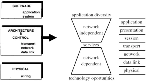
1.2 The Design Abstraction Levels of Network-on-Chip
The topic of Network-on-Chip(NoC) designs is vast and complex. Consider on-chip communication and its abstraction of network-on-chip as a micro-network and analyze the various levels of the micro-network stack bottom to up as right part in Figure 1.4, starting from physical layer to software layer [33]. NoC protocols are typical organized in layers which is similar to the OSI protocol stacks as the left part in Figure 1.4[34]. For a micro-network, the protocol stack will be reduced to physical layer, data-link layer, network and transport layer and software layer [35].The characteristics of each layer will be described in this section.
NoC protocols are described bottom-up, starting from the physical up to the software layer. In the physical layer, global wires are the physical implementation of the communication channels. Traditional rail-to-rail voltage signaling with capacitive termination is definitely not well-suited for high-speed, low-energy communications for future global interconnect. Reduced swing can significantly reduce communication power dissipation which preserves the speed of data communication. Nevertheless, as the technology trends lead us to use smaller voltage swings and capacitances, the upset probabilities will rise. It is important to realize that a well-balanced design, because the overhead in performance, energy-efficiency and modularity may be too high. Physical layer design should find a compromise between competing quality metrics and provide a clean and complete abstraction of channel characteristics to micro-network layers above.
The data-link layer abstracts the physical layer as an unreliable digital link, where the probability of bit upsets is non null. Furthermore, reliability can be traded off for energy. The main purpose of data-link protocols is to increase the reliability of the link up to a minimum required level, under the assumption that the physical layer by itself is not sufficiently reliable. At the data link layer, error correction can be complemented by several packet-based error detection and correction protocols. Several parameters in the protocols can be adjusted depending on the goal to achieve maximum performance at a specified residual error probability within given energy consumption bounds.
At the network layer, packet data transmission can be customized by the choice of switching and routing algorithms. The NoC designers establish path of connection
to its destination. Switching and routing affect heavily performance and energy consumption. Robustness and fault tolerance will also be highly desirable. At the transport layer, algorithms deal with the decomposition of messages into packets at the source and their assembly at destination. Packetization granularity is a critical design decision because the behavior of most network control algorithm is very sensitive to packet size. Packet size can be application specific in SoCs, as opposed to general network.
Software layers comprise system and application software which includes processing element and network operating systems. The system software provides us with an abstraction of the underlying hardware platform. Moreover, policies implemented at the system software layer request either specific protocols or parameters at the lower layers to achieve the appropriate information flow. The hardware abstraction is coupled to the design of wrappers for processor cores which perform as network interfaces between cores and NoC architecture.
1.3 Research Motivation
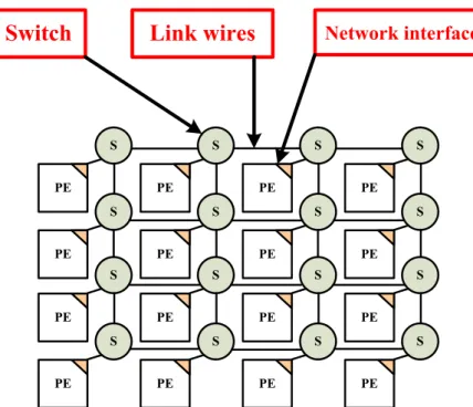
A simple mesh architecture of Network on Chip is shown in Figure 1.5. This research focuses on physical layer and data-link layer of NoC protocols. The goal of this research is to achieve a low latency, low power and reliable interconnect architecture. The architecture will be applied to each transmission stage between two adjacent switchs. The design of NoC protocols should consider each stage properties together to achieve better performance. Based on this concept, we adopt serialization technique to implement packet-based transmission, which is the most significant difference of Network-on-Chip architecture to other on-chip bus approachs.
PE S PE S PE S PE S PE S PE S PE S PE S PE S PE S PE S PE S PE S PE S PE S PE S
Switch
Link wires
Network interfaceFigure 1.5: A simple architecture of Network on Chip
The traditional rail-to-rail voltage signaling will be no longer suitable for low power interconnect design. Reduced signal swing can significantly reduce power consumption on link wires. However, as the technology trends lead us to smaller voltage swings and larger coupling capacitances effect, it means the interconnect will be more suspect to muti-noise sources in future. It is important to carefully design and tradeoff each performance metrics. To guarantee the reliability is considered a necessary and important issue especially in future nanometer design. Furthermore, reliability can be traded off for energy. According to this concept, we want to save more energy on link wires based on guaranteed reliability bound. The whole architecture should tolerant to process-variation, to make sure the circuits functional work in different cases.
1.4 Organization of Thesis
The rest parts of thesis are organized as follows: In Chapter 2, we mention the background of nanometer interconnects. Two high performance signaling modes are introduced. The low power design concept of on-chip interconnect is introduces. Finally, we mention the advantage of using serialization technique for link wires. In Chapter 3, a unified framework of joint coding scheme concept is introduced and some previous related work of different coding schemes is listed. The proposed
self-corrected green coding scheme based on triplication bus model is presented in
this Chapter also. In Chapter 4, a self-calibrated voltage scaling technique for reliable Interconnections in Network-on-Chip is proposed. The concept of high error coverage and low test overhead MAF-based test mechanism and process-variation aware modify double sampling data checking technique are introduced. According to these schemes, we show how the voltage scaling technique able to tradeoff energy and reliability. In Chapter 5, simulation result and related analyses is presented. Compare to other coding approach on energy saving to un-coded word and error-rate analysis. Also the process-variation aware on link wires in different transmission cases is presented. Finally, conclusion is summarized in Chapter 6.
Chapter 2
Background
2.1 Nanoscale interconnect
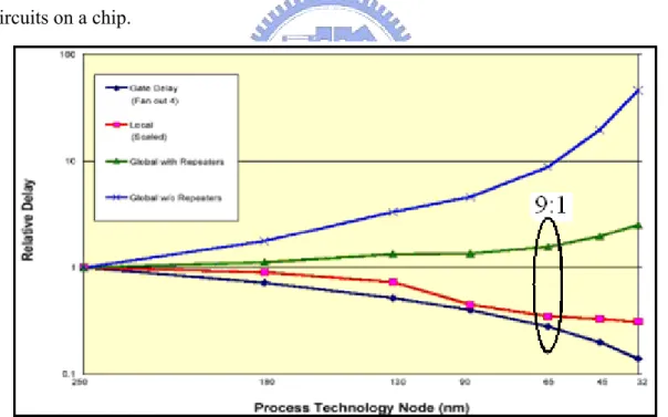
According to ITRS prediction illustrated in Figure 2.1, the gate between the interconnection delay and the gate delay will increase to 9:1 with the 65nm technology [36]. Increasing of power dissipation consumed in charging and discharging the interconnect wires on a chip. Soon the interconnect will domain the performance such as power consumption, speed, and area. It means that interconnection will affect the system more in future SoC design rather than logic circuits on a chip.
Figure 2.1: Relative delay comparison of wires versus process technology
New design approach like network on chips (NoC) provides a more process independent interconnection architecture. However, we still need to understand more detail physics effect in the on-chip interconnect of Deep-Sub-Micron technology.
Four factors are referred to cause new challenges in DSM [37]: (1) Increasing of operation frequency so that the inductance effect can’t be ignored anymore. (2)Signal reflection and transmission due to impedance mismatch. (3)Increasing of fringe capacitance due to increased aspect ratio of the interconnection wire. (4) Increasing of resistance due to skin effect of high frequency and contact resistance.
The signal integrity is an important issue for on-chip interconnect. The degradation comes from many different source, intrinsic RLC circuit nature and extrinsic noises. Intrinsic RLC circuit nature such as RC delay, LC ringing, attenuation of wave amplitude .etc. Extrinsic noises such as crosstalk noise inter-symbol interference (ISI ). The wave overlapping cause ISI and leads to higher error rate on interconnect. The most significant noise in DSM is crosstalk noise. Through the coupling capacitance, the delay and skew of victim line signals can be affected by adjacent lines (aggressor lines). Crosstalk noise makes difficult to estimate the exact delay deviation.
Interconnect capacitance/resistance became comparable to gate in today’s technology. Significant inductance effects with technology scaling in the future. In DSM, the inductance effect of wires becomes a noise source. When aggressor lines are switching simultaneously, the filed electromagnetic may induces noise on the victim lines. The effect of inductance can be neglected if f << R/(2πL) in most case of on-chip interconnect. According to the simulation results of [38], the inductance effects will change the worst case (delay consideration) transition for nano-scale interconnect wires only when the operation frequency is over 1GHz. We will ignore the inductance effect of on-chip interconnect in this thesis.
2.2 High Performance Signaling
2.2.1 Voltage-mode & Current-mode Signaling
Generally speaking, there are two modes for high performance signaling : Voltage-mode signaling and Current-mode signaling. As shown in Figure 2.2(a), voltage-mode signaling using CMOS inverters as driver and receiver. The load capacitances of wire are charged/discharged by driver. The receiver is active until voltage of receiver’s input node have been charged/discharged to full-level swing. The voltage-mode signaling is a simple and conservative way of signaling. No static current dissipation, so the power consumption of voltage-mode signaling is proportional to the switching activity of signals. However, driving longer interconnect needs larger driver size, the related work such repeater insertion technique have been proposed to solve the problem. Some paper discussed the optimal numbers and size of repeaters and the optimal wire length and wire segments [39-41]. Try to tradeoff between performance metrics, such as delay, power .etc.
Current-mode signaling circuits as shown Figure 2.2(b).With the same driver circuits as voltage-mode signaling, the current charge the load capacitance of wire. Current flows through load resistance Mp and Mn. The receiver don’t have to wait the input node of it charged to VDD, it can detect the small voltage at the load resistance changed by the current flow. The current-mode signaling is faster than voltage-mode signaling, because it doesn’t need a full swing level charge/discharge to decide logic value. The maximum data rate of a current-mode signaling is about twice of voltage-mode signaling if two schemes have same number of repeaters. When the load capacitance is large, it seems that the current-mode signaling can achieve better power efficient than voltage-mode signaling. Major portion of power consumption in
current-mode signaling is due to static current ( I2 , as shown in Figure 2.2(d) ) through the wires. If the switching activity of signal is 0.5, current-mode signaling can save about 25% power from voltage-mode signaling. However, if the switching activity of signal is less than 0.4, the voltage-mode signaling is better than current-mode signaling on power saving. Because current-mode signaling don’t charge to full-level swing, the scheme is susceptible to noise sources.
I
1+
V
1+
V
2 Mp Mn0
Static current (I
2)
V
1I
1V
2I
2(a)
(b)
(c)
time(d)
time Figure 2.2: (a)Voltage-mode (b)Current-mode signaling circuits2.2.2 Low Power Interconnect Design
Low power design been emphasized in future design. The power consumption of on-chip interconnect can be simply described as :
P
= ×
α
C
w×
V
swing×
VDD
driver×
f
(2.1)where α is the switching activity of signal, Cw is the wire capacitance , Vswing is the
voltage swing on the wire, VDDdriver is the supply voltage of the driver and f is the
signaling frequency. To design a lower power interconnect, we can minimize each of parameters ( α, Cw , Vswing , VDDdriver , and f ) in Equation (2.1).
(1) Reducing the switching activity
Switching activity α can be reduced by coding schemes. Low power codes (LPC) are first proposed to achieve the goal, such as bus-invert (BI) code [42], partial BI code [43], T0-code [44] and Gray-code [45]. Gray-code and T0-code reduce the switching activity of address bus effectively because the data in the address bus is sequential, But these two schemes is not suitable for data bus. However, these schemes just consider self transitions but ignored coupling capacitances effect. Crosstalk avoidance codes (CAC) that reduce both self and coupling transitions by forbidding specific transitions, such as Forbidden Overlap Codes (FOC), Forbidden Transition Codes (FTC), Forbidden Pattern Codes (FPC) and One Lambda Codes (OLC) [46-48].
(2) Reducing wire capacitance
In DSM technique, the coupling capacitance will domain the value of equivalent total capacitance. Simply way to reduce wire capacitance techniques is widening the spacing between two adjacent wires. To minimize the wiring area, on-chip serialization technique is an effective way, which will be discussed in Section 2.3.
(3) Reducing voltage swing of signal
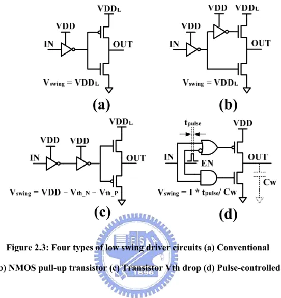
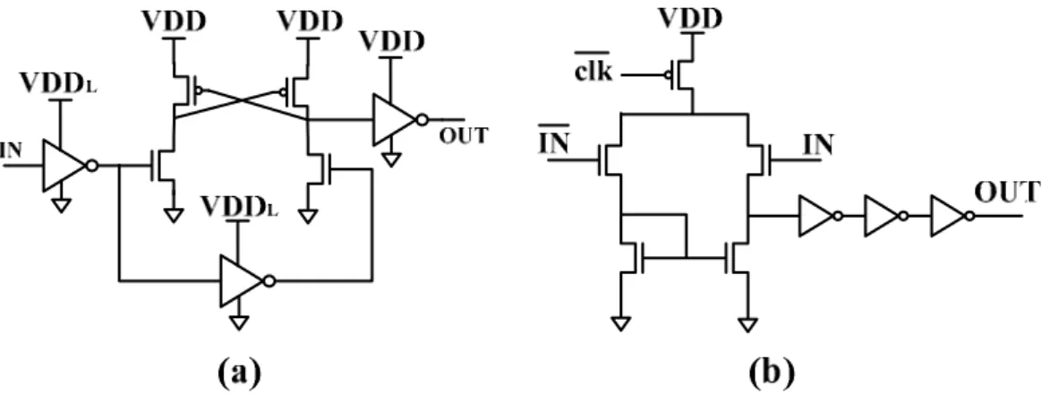
Low-swing signal and supply voltage can reduce the power consumption of on-chip interconnect significantly. The swing level of signal must carefully design because it is related to signal noise immunity. Many low-swing schemes was discussed in [], we will introduced some receiver circuits and receiver circuit following.
Four types of low-swing driver as shown in Figure 2.3 . Driver circuits as shown in Figure 2.3(a) and Figure 2.3(b) are able to reduced power to (VDDL/VDD)2, where
VDDL is additional reference voltage source. The additional reference voltage source
is produced by off-line DC-DC convert. Driver circuit as in Figure 2.3(c) has a signal voltage swing equal to by a voltage drop Vt of transistor. Driver circuit as in Figure 2.3(d) use pulse to control the charge/discharge time on wire load capacitance, the signal voltage swing is equal to . But the value of wire load capacitance is hard to be estimated during design stage. The advantage of driver circuits as shown in Figure 2.3(c) and Figure 2.3(d) is they don’t need extra reference voltage source, but with the disadvantage of the circuits are susceptible to process variation and need re-design in different technology node.
th_N th_P
VDD-V -V
*
pulse/
Figure 2.3: Four types of low swing driver circuits (a) Conventional (b) NMOS pull-up transistor (c) Transistor Vth drop (d) Pulse-controlled
The low swing receiver design can be implemented in two ways: single-ended conventional level converter as shown in Figure 2.4(a) and differential amplifier as shown in Figure 2.4(b). Differential signaling has better noise immunity, but requires double the numbers of wire. In [49], the author consider different receivers in respect of energy, delay, signal swing level, signal-to-noise ratio and complexity. The driver/receiver circuit implemented to on-chip network should as simple as possible. We adopt conventional type of driver circuit and single-ended level converter as receiver. Without an additional reference voltage source, the VDDL is produced by
CMOS diode-connected voltage drop scheme, more detail will be introduced in Chapter 4. Maybe the different type of driver/receiver circuits can achieve better performance in specific metric, but it isn’t the key point in this thesis.
Figure 2.4: Two types of low swing receiver circuits (a)Single-ended level converter (b) Differential amplifier
2.3 Serialization Technique For Link Wires
The physical transfer unit is a unit into which a packet is divided and transmitted through micro-network. Simply speaking, the phit size is the bit-width of the link wire, I/O and switch size. Large phit size increases network area and energy consumption, especially for switching circuit and buffering units in switch fabrics. Some approaches address signal integrity to protect the NoC interconnection infrastructures against different transient malfunctions [50,51]. However, these approaches could not decode the encoded codes in each switch fabric because of significant delay. The critical depth, moreover, will increase rapidly as well as the bit-width increases. Therefore, the un-decoded code will induce great amount of area and energy dissipation of switching circuits and buffers in switch fabrics.
Joint coding schemes have been consider the effective way to reduce power consumption and at the same time provide a reliable interconnect. However, both
crosstalk avoidance codes and error correction codes enlarge the physical transfer unit (phit) in network-on-chip. According to the disadvantages mention above, we can joint bus and error correction coding scheme with concept of serialization and deserialization technique. Figure 2.5 show a K-to-N serialization with N:1 ratio. Serialization ratio is defined as I/O bit width divided to phit size. Original data without serializer was sent K bit each cycle, but was sent K/N bit each cycle with serializer. The serializer and deserializer reduce the phit size and further reduce the area and energy consumption of the switch fabrics. However, in order to achieve the same throughput, the serialization technique will increase the operation frequency of interconnection network. On-chip serialization, nevertheless, is a crucial technique for NoC implementation. It reduces overall network area and optimizes power consumption which is well-explained in [52,53].
Figure 2.5: K-to-N serialization with N:1 ratio
Figure 2.6(a) and 2.6(b) are simulated under high loading and low loading of wires, respectively. Despite of loading, the power consumption decreases with the increasing ratio of serializer under low operation frequency. Unfortunately, with he increasing ratio of serializer under higher operation frequency, the power consumption increases because of large driver to provide high driving ability.
Figure 2.6: Average power versus different ratio of serializer and frequency (a) in high loading (b) in low loading of wires
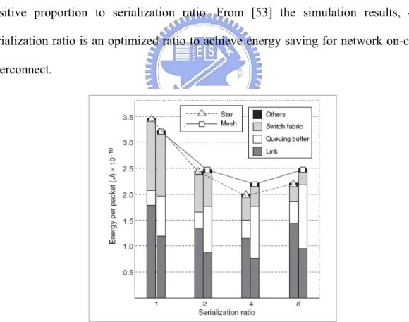
Figure 2.7 shows that the switch and link energy consumption decrease effectively depend on serialization ratio. But queuing buffer energy consumption increase positive proportion to serialization ratio. From [53] the simulation results, 4:1 serialization ratio is an optimized ratio to achieve energy saving for network on-chip interconnect.
Figure 2.7: Energy variation in relation to serialization ratio when the number of processing units (N) = 16 under Mesh and Star NoC topology [53].
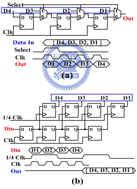
We implemented the serializer and deserializer with all-digital self-calibrated multi-phase delay-locked loop in [54]. The shift register based serializer/deserializer architecture was adopted in this thesis, implemented by low swing edge-triggered Flip-Flop. 4-to-1 Serializer circuit and waveform as showed in Figure 2.8(a), and 4-to-1 deserializer circuit and waveform as showed in Figure 2.8(b). The data can operate in quarter of clock frequency. Reducing operation frequency can achieve power saving goal.
Figure 2.8: (a) Shift Register Based Serializer and waveform (b) Shift Register Based Deserializer and waveform
Chapter 3
Self-Corrected Green Coding Scheme
3.1 Preliminary
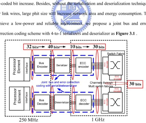
Joint coding schemes based on the unified framework provide better communication performance. However, the schemes mention above just combine different kinds of codes directly. The intrinsic qualities of crosstalk avoiding coding and error correction coding are mutually exclusive, except for duplicate-add-parity (DAP). The previous works have disadvantages of encoder/decoder hardware overhead, encoder/decoder need a significant propagation delay when numbers of un-coded bit increase. Besides, without the serialization and deserialization technique for link wires, large phit size will increase network area and energy consumption. To achieve a low-power and reliable interconnect, we propose a joint bus and error correction coding scheme with 4-to-1 serializers and deserializer as Figure 3.1 .
Pr o c e s s o r El e m e n t in te rf a c e in te rf a c e ECC de co d e r EC C enc od e r P roc es s o r El e m e n t
Figure 3.1: A joint bus and error correction coding scheme with serializers/deserializer in network-on-chip
In this chapter, we focus on the joint bus and error correction coding scheme, self-corrected green coding scheme. To realize reliable and green interconnection for NoC platforms. Self-corrected green coding scheme is constructed by two stages, which are green bus coding stage and triplication ECC stage. The green bus coding is developed by the joint triplication bus power model to achieve more energy reduction for the triplication ECC. The detail of self-corrected green coding scheme will be described in the following section. It has the characteristics of shorter delay for ECC, more energy reduction and smaller area.
3.2
A Unified Framework of Joint Coding Scheme
For on-chip interconnection, three main problems have to been considered, which are delay, power and reliability. For the delay problem, large propagation delay due to capacitive. Especially long global line, low swing voltage to charge capacitive take a long time. High power consumption of interconnects is due to both parasitic and coupling capacitance. Finally, reliability depends on increased susceptibility to errors due to noise. In advanced technologies, circuits and interconnects become more sensitive to noises as to the lower operation voltage. In addition, the increasing coupling noise, soft-error rate, bouncing noise decrease the reliability also. In view of this, self-calibration circuitry is essential in today’s SoC design. Therefore, coding theory is an effective solution to deal with the three challenges. Joint bus and error correction coding has been an elegant and effective technique to solve the crosstalk effect and further provides a reliability bound for on-chip interconnect.
(1) LPC (Low-Power Codes): Reducing transition activity to achieve low power interconnect.
(2) CAC (Crosstalk Avoidance Codes): Avoid specific code patterns or code transitions to reduce delay and power dissipation produced by crosstalk effect. (3) ECC (Error Control Codes): To guarantee error-free transmission, the code has
to provide a reliability bound. The code is able to detect or correct the error bits.
LPC and CAC are hard to separate completely, because they have some similar properties. Sometimes avoid crosstalk between lines will also lower the power consumption. To briefly sum up, LPC and CAC Reducing transition activity and forbidding some transitions which cost large power.
Joint codes architecture have been proposed in [14]. An unified coding framework as shown in Figure 3.2, it’s rules are:
(1) CAC needs to be the outermost code (2) LPC can follow CAC
(3) ECC needs to be systematic
(4) The additional information bits generated by LPC (p) and ECC (m) need to be encode through linear crosstalk code (LXC1/LXC2)
3.2.1 Related Work On Crosstalk Avoidance Codes
Crosstalk avoidance codes (CACs) can be used to improve signal integrity and also reduce the coupling capacitance effect and hence the reduce energy dissipation of wire segments. CACs reduce the worst-case switching patterns of a wire by ensuring that transition from one codeword to another codeword does not cause adjacent wires to switch in opposite directions . According to the analysis in [18] for the specific case of on-chip buses, the bus lines must be 20mm longer in order for these encoding schemes to be energy efficient in practical implementations. Due to the NoC design, the wire segments between two routers or between router and IP are significantly shorter than the above mentioned limit. [55].
The purpose of crosstalk avoidance code is to reduce the delay of the line to (1+pλ)τ, where p = 1,2 or 3 depend on the maximum coupling (worst case delay (1+4λ)τ ). The following consider four CACs: Forbidden Overlap Codes, Forbidden Transition Codes, Forbidden Pattern Codes and One Lambda Codes. These CACs achieve different degrees of delay reduction.
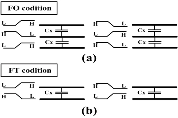
First, we define three conditions which help us to analysis the switching activity of codeword, named Forbidden Overlap condition, Forbidden Transition condition and Forbidden Pattern condition. Forbidden Overlap condition represents a codeword transition from 010 to 101 or from 101 to 010 as shown in Figure 3.3(a). Forbidden Transition condition represents a codeword transition from 01 to 10 or from 10 to 01 as shown in Figure 3.3(b). Forbidden Pattern condition represents a codeword having 010 or 101 patterns.
Figure 3.3: (a) Forbidden Overlap condition (b) Forbidden Transition condition
(1) Forbidden Overlap Codes (FOC)
Maximum coupling can be reduced to p=3. The FOC can be satisfied if and only if a codeword having the bit pattern 010 (or 101) does not make a transition to a codeword having the pattern 101 (or 010) at the same bit positions. Encoding all the bits at once is not feasible for wide links due to size and complexity of the codec hardware. Considering a 4-bit sub-channel the coding scheme shown in Table 1(a). For coding 32 bits, eight FOC4-5 blocks are needed, and 32-bit un-coded link will be converted to a 40-bit coded link. In this case two sub-channels can be placed next to each other without any shielding, as well as not violating the FO condition.
(2) Forbidden Transition Codes (FTC)
Maximum coupling can be reduced to p=2. The FTC can be satisfied by ensuring that the transitions between two successive codes do not cause adjacent wires to switch in opposite directions (i.e., a codeword has a 01 bit pattern, the subsequent
codeword cannot have a 10 pattern at the same bit position ) Considering a 3-bit sub-channel the coding scheme is expressed in Table 1(b). In this case also we combined the sub channels in such a way that there is no forbidden transition at the boundaries between them. Consequently a 32-bit un-coded link will be converted to 53-bit coded link.
(3) Forbidden Pattern Codes (FPC)
Maximum coupling can be reduced to p=2. FPC codes can be achieved by avoiding 010 and 101 bit patterns for each of the code words. Considering a 4-bit sub-channel the coding scheme is expressed in Table 1(c). Consequently a 32-bit uncoded link is converted to a 52-bit coded link.
(4) One Lambda Codes (OLC)
Maximum coupling can be reduced to p=1.OLC codes satisfy the Forbidden adjacent boundary pattern condition: two adjacent bit boundaries in the codes cannot both be of 01-type or 10-type. Besides, OLC also avoid FT and FP condition. The simplest OLC is duplication and shielding, where every bit is duplicated and shield wires are inserted between adjacent pairs of duplicated bits [17]. However, OLC encode k-bits un-coded bits to l=11 / 4 3k − bits. For example, 85wires are
Table. 1: (a) FOC4-5 coding schemes (b) FTC3-4 coding schemes
3.2.2 Related Work On Error Control Codes
Incorporating of different coding schemes in SoC design is being investigated as a means to increase system reliability. We know CACs reduce the worse-case switching capacitance of a wire by ensuring that a specific codeword transitions doesn’t happen. However, NoC is sensitive to internal (power supply noise, crosstalk noise, inter-symbol interference ) and external (electromagnetic interference, thermal noise , noise by alpha particles) noise source due to lower supply voltage, smaller node capacitances, decreasing of inter-wire spacing, the increasing role of coupling capacitances, the higher clock frequency ..Etc.
CACs don’t help to against these noises. To make the system robust, CAC incorporate with forward error correction coding is a solution. Jointing CAC and single error correction (SEC) codes such as: Duplicate-add-parity (DAP) and Modified Dual Rail (MDR) [14,50], Boundary Shift Code (BSC) [16] and Hamming codes[56]provide on-chip interconnect better reliability.
(1) Duplicate-add-parity (DAP) and Modified Dual Rail (MDR):
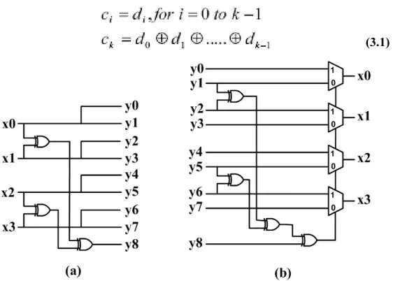
Encoder/Decoder of Duplicate-add-parity as shown in Figure 3.4. Encoder duplicates data( x0,x1,x2,x3 ) and generates ( y0,y2,y4,y6 ), y8 is parity bit generate from x0 x1 x2 x3 whic♁ ♁ ♁ h means if data has odd numbers of “1” y8=1, else (even numbers of “1”) y8=0. Decoder receive data y0~y7 and former stage parity bit y8. Comparing y8 with new parity y1 y3 y5 y7♁ ♁ ♁ on the Decoder sides, if two parity is identical, multiplexer is selected by “0” and get decode data ( y1,y3,y5,y7 ) . Else two parity is different, multiplexer is selected “1” and get data ( y0,y2,y4,y6 ). This scheme has ability to correct one-bit error.
The Modified Dual Rail (MDR) code is very similar to the DAP. In the Dual Rail (DR) code, considering a link of k information bits, m = k + 1 check bits are added, leading to a code word length of n = k + m = 2k + 1. We define the k + 1 check bits with Equation (3.1). In the MDR two copies of parity bit Ck are placed adjacent to the other codeword bits, to reduce crosstalk.
(3.1)
Figure 3.4: Duplicate-add-parity code (a) Encoder (b) Decoder
(2) Boundary Shift Code (BSC):
The following will introduce Boundary-Shift Code and give an example. Boundary-Shift Code is generated by copying each bit and adding a parity bit to show the input bits have odd or even numbers of “1”. Besides, the parity bit will shift between first bit and last bit of output each transition cycle time as shown in Table 2.
Table 2: Example for Boundary-Shift Code.
Boundary-Shift Code Decoding is done by majority vote; two “copies” of the desired bit and third bit are generated by sum (mod2) of copy of each of other information bits and parity bit. For example y0, y1, and (y2+y4+y6+y8) mod-2 as Shown in Table 3 blue marks. The red marks as shown in Table 3 are error output bits, Table 3 shows an example that BSC is able to correct one error in cycle 1~3 (no matter one error is occurred at data bit or parity bit ), but will fail in cycle 4 when there are two errors or more errors occurred.
Table 3: Example of Boundary-Shift Code error correct ability
Boundary-Shift Code Encoder and Decoder as shown in Figure 3.5, it shows that BSC has disadvantages of large gate numbers and critical path which depend on
transmission bit. For n-bits un-code data, it is encoded to (2n+1) bits, the circuit depth of encoder and decoder are
[
log2n]
+1 and ⎣⎡log2(
n+1)
⎤⎦+1 respectively [16].Figure 3.5: Boundary Shift Code (a) Encoder (b) Decoder
(3) Hamming code[56]
Traditional error control code such as Binary (7, 4) Hamming code, if transfer 4-bits data (m1, m2, m3, m4), it needs redundant 3 Parity bits as information to detect which bit error and have ability to correct one error. Parity bit Pi is 0 or 1 to make the number of 1s in the set (Pi, mx, my, mz) even. So, the parity is given by Pi = mx♁my♁mz. The complexity of (7,4) Hamming encoder is 5XOR2, and the propagation delay is 2XOR2. The complexity of (7,4) Hamming decoder is 12XOR2+4NAND3+3Inverters, and the propagation delay is 5XOR2. Figure 3.6 shows the encoder, syndrome generator and decoder of (7,4) Hamming code.
At system level, for 32 bit word use binary systematic (38, 32, 3) code, known as extend Hamming code to correct a single error. The parity bits of binary systematic (38, 32, 3) codes are given by (P1, P2, P3, P4, P5, P6) as shown in Equation (3.2), where mi denote data bits and Pi denote parity bits. The complexity of (38, 32, 3) encoder is 70XOR2, and the propagation delay is 5XOR2. The complexity of (38, 32,
3) decoder is 108XOR2+96 NAND3+6Inverters, and the propagation delay is 8.5XOR2. The results shows that Hamming code with large hardware overhead and propagation delay which may degrade the performance of on-chip interconnect.
Figure 3.6: Hamming Code (a) Encoder (b) Syndrome generator (c) Decoder P1=m1 m2 m4 m5 m7 m9 m11 m12 m14 m16 m18 m20 m22♁ ♁ ♁ ♁ ♁ ♁ ♁ ♁ ♁ ♁ ♁ ♁ m24 m26 m27 m29 m31 ♁ ♁ ♁ ♁ ♁ P2=m1 m♁ 3 m4 m♁ ♁ 6 m7 m♁ ♁ 10 m11 m1♁ ♁ 3 m14 m1♁ ♁ 7 m18 m2♁ ♁ 1 m22 m2 ♁ ♁ 5 m26 m2♁ ♁ 8 m29 m3♁ ♁ 2 P3=m2 m♁ 3 m4 m♁ ♁ 8 m♁ 9 m♁ 10 m11 m1♁ ♁ 5 m1♁ 6 m1♁ 7 m18 m2♁ ♁ 3 m2 ♁ 4 m2♁ 5 m26 m♁ ♁ 30 m♁ 31 m3♁ 2 P4=m5 m♁ 6 m♁ 7 m♁ 8 m♁ 9 m♁ 10 m11 m1♁ ♁ 9 m♁ 20 m♁ 21 m♁ 22 m2♁ 3 m2 ♁ 4 m2♁ 5 m2♁ 6 P5=m12 m♁ 13 m♁ 14 m♁ 15 m♁ 16 m♁ 17 m1♁ 8 m1♁ 9 m♁ 20 m♁ 21 m♁ 22 m2 ♁ 3 m2♁ 4 m2♁ 5 m2♁ 6 (3.2) P4=m27 m♁ 28 m♁ 29 m♁ 30 m♁ 31 m♁ 32
With aggressive supply voltage scaling and increase in deep sub micron noise, single error correcting codes will not satisfy the reliability requirements. More powerful ECC (such as multiple error correcting) will need in future NoC design.
3.3
Proposed Self-Corrected Green Coding Scheme
3.3.1 Triplication Error Correction Coding Stage
The triplication error correction coding scheme as shown in Figure 3.7 is a single error correcting code by triplicating each bit. From the information theory, it is well-known that a code set with hamming distance of h has h-1 error-detect ability and [(h-1)/2] error-correct ability. For the triplication error correction coding, the hamming distance of each bit is equal to 3. Therefore, each bit can be corrected by itself if there are no more than two error bits in the three triplicated bits. The error bit can be corrected by a majority gate, and the function of the majority gate is shown in Figure 3.7. Compared to other error correction mechanisms, the critical delay of the decoder is a constant delay of a majority gate and much smaller than other ECCs. In other words, it has rapid correction ability by self-corrected in bit level. Therefore, triplication error correction coding is more suitable in network-on-chip for smaller encode/decode propagation delay.
In addition, one of the advantages of incorporating error correction mechanisms in the NoC data stream is that the supply voltage of channels can be reduced without compromising the reliability of system. Reducing the supply voltage Vdd will increase the bit error probability. To simplify the error sources, we assume the bit error probability ε is as Equation (3.3) when a Gaussian distributed noise voltage VN with variance σN2 is added to the signal waveform.
2 dd n V Q
ε
σ
⎛ ⎞ = ⎜ ⎟ ⎝ ⎠ (3.3) Where Q(x) is given as( )
2 21
2
y xQ x
e
dy
π
∞ −=
∫
(3.4)Each triplication sets can be error-free if and only if no error transmission or just 1-bit error transmission. For each triplication sets, therefore, P1-bit correct is given as
(
)
3(
)
2 13
1
1
1
bit correctP
−= −
ε
+
⎛ ⎞
⎜ ⎟
ε
−
ε
⎝ ⎠
(3.5)For k-bits data, transmission is error-free if and only if all k triplication sets are correct. Pk-bits-correct is given by
(
2 3)
1
1 3
2
k k
k bit correct i bit correct i
P
−P
−ε
ε
=
=
∏
= −
+
(3.6)Hence, the word-error probability will be
(
2 3)
1 1 3
2
ktriplication
P
= − −
ε
+
ε
(3.7)For small probability of bit error ε, Equation (14) simplifies to
(3.8)
2 3
3
2
self correct
P
−=
k
ε
−
k
ε
By contrast, the word-error probability is much smaller than Hamming code and DAP which are direct to k2ε2. The triplication error correction coding, moreover, can
avoid forbidden overlap condition (FOC) and forbidden pattern condition (FPC) which will induce large energy dissipation by coupling effect. The FO condition can be defined that bit pattern (y2,y1,y0) does not have transition from 010 to 101 or from 101 to 010. And forbidden pattern condition can be satisfied that avoiding bit pattern 010 and 101 in (y2,y1,y0).
3.3.2 Joint Triplication Bus Power Model
The bus model proposed by [57] by considering the loading capacitances and coupling capacitances. Figure 3.8(a) shows the model which are modified for four bits bus. The Cii means the loading capacitance of line i and the Cij is the coupling capacitance between line i and line j. Moreover, the bus lines are laid parallel and coplanar. Most of the electric field is trapped between the adjacent lines and the ground. An approximate deep submicron bus power model with ignoring the parasitic between nonadjacent lines is as Figure 3.8(b).
Figure 3.8: (a)Bus model for four bits (b)The approximate bus model
We assume all grounded capacitors which have the same value without considering the fringing effect of the boundary lines. Because of the fringing capacitors are much less than the loading and coupling ones, even more for the wide buses. From Figure 3.8(b), we can define the capacitance matrix Ct as Equation (3.9):
(3.9) L X L t
C
C
C
C
=
⎥
⎥
⎥
⎥
⎦
⎣
0
0
−
λ
1
λ
⎤
⎢
⎢
⎢
⎢
⎡
+
−
+
−
−
+
−
−
+
=
λ
λ
λ
λ
λ
λ
λ
λ
λ
,
1
0
0
1
0
0
1
The parameter λ is defined as the ratio of coupling capacitance to loading capacitance. Therefore, the parameter depends on the technology as well as the specific geometry, metal layer and shielding of the bus. It has some properties such that the parameter λ tends to increases with technology scaling. For instance, λ is between 3 and 6, depending on the metal layer for standard 0.13um CMOS technology and minimum distance between the wires. The parameter λ is expected much lager in advanced technology.
Between two adjacent lines, there are five types of transition states, and four of them are mentioned in [58]. The five types can be separated into two cases: the first case is static transitions like type I (single line switching) type II (two lines switching in opposite direction) and type III (no switching) in Figure 3.9. And the other one is dynamic transitions as type IV and type V with signals aliasing in Figure 3.9. The static transition is defined as that the two adjacent lines switch at the same time without noises and different delays. The dynamic one means the two adjacent lines having possible misalignment.
Figure 3.9: Five transition types for two adjacent wires
Although triplication error correction coding can avoid some forbidden conditions, some power-hungry transition patterns can not be avoided completely. These patterns are mainly constructed by Forbidden Transition condition and self switching activity. The FT condition can be satisfied that bit pattern (y1,y0) does not have transition from 01 to 10 or from 10 to 01. Therefore, we presented a joint triplication bus model to implement the bus coding stage for achieving more energy reduction. For 4-bit triplication bus, the capacitance matrix Ct can be expressed as Equation (3.10).
3
0
0
3 2
0
,
0
3 2
0
0
3
t x L LC
C
C
C
λ
λ
λ
λ
λ
λ
λ
λ
λ
λ
λ
+
−
⎡
⎤
⎢
−
+
−
⎥
⎢
⎥
=
=
⎢
−
+
−
⎥
⎢
−
+
⎥
⎣
⎦
(3.10)The parameter λ is defined as the ratio of coupling capacitance Cx to loading capacitance CL. The capacitance matrix is modified from [59] and the coefficient of
loading capacitances is 3 for triplicated bits. Therefore, the power consumption formula is shown in Equation (3.11). E and P represent energy and power density respectively. Then, f and V (VDD) are frequency and voltage (voltage supply). Bi means the current transition state (1 or 0) for the line i, and Bi-1 shows the previous state for the line i.
( ) (
f T t f i)
E
=
V
C V
−
V
(
) (
)
{
}
2 t 1 DD i i j j i jP
= ∗
f V
∗
∑∑
C
B
−
B
−∗
B
−
B
−1 (3.11) The power density P can be transferred to Equation (3.12).(
) (
) (
)
(
)
(
) (
)
(
) (
)
(
) (
)
2 2 1 1 1 1 2 2 3 3 2 2 1 1 4 4 1 1 2 2 2 2 1 1 2 2 3 3 2 1 1 3 3 4 43
3
3
3
L DDB
B
B
B
B
B
B
B
B
B
B
B
P
f
C
V
B
B
B
B
B
B
B
B
λ
λ
λ
− − − − − − − − −⎧
−
+
−
+
−
⎫
⎪
⎪
⎪
⎪
2 1 1 −⎡
⎤
+
−
+
−
−
−
⎪
⎣
⎦
⎪
⎪
⎪
= ∗
∗
∗ ⎨
⎬
⎡
⎤
⎪
+
⎣
−
−
−
⎦
⎪
⎪
⎪
⎪
+
⎡
−
−
−
⎤
⎪
⎪
⎣
⎦
⎪
⎩
⎭
(3.12)The items of Equation (3.12) are defined and identified as follow:
1 2 1 1 1 2 1 1 1
(
)
[(
) (
)]
4
i i i i i i i j j i j ij i i j j i i j jB
B
B
B
r
B
B
B
B
r
r
d
where d
B B B B
B B B B
− − − − − − − −−
=
⊕
=
−
−
−
= ⊕ + ×
=
∪
1 ij (3.13)What the ri means is that there is a switch of line i. It does not concern about the
direction of the change and the adjacent lines. This item is only considering about the loading capacitances. The meaning of ri⊕rj is that only one line is changing between
direction. Moreover, comparing with the other two definitions, ri and ri⊕rj, the
voltage difference across the coupling capacitance is double and when squared it results in power 4 times. This explains the factor 4 for dij. And using Equation (3.14),
we can get the power formula as Equation (20) with the parameter of λ. The term α is the coefficient about coupling effects and switching activities.
2 1 2 3 4 1 2 2 3 3 4 12 23 34
3(
)
(
)
4 (
)
L DDP
f
C
V
r
r
r
r
r
r
r
r
r
r
d
d
d
α
α
λ
λ
= ×
×
×
=
+ + +
+
⊕ + ⊕ + ⊕
+
+
+
(3.14)3.3.3 Green Bus Coding Stage for Crosstalk Avoidance
The purpose of green bus coding is to minimize the value of α in Eq. (19) by encoding the signals when λ>2, the design flow of green bus coding as shown in Figure 3.10.
Therefore, we establish a 32x32 transition state table by calculating α, Table 4 shows the total α value of each patterns transit to other 31 patterns. So we can select 16 transition patterns with minimal values of α as the codeword by avoiding crosstalk. The 16 patterns is composed of 2 with α_total =400, 8 with α_total =528 (blue mark as shown in Table 4), and 6 with α_total =656 (select from 12 patterns, red mark as shown in Table 4). 00000 00001 00010 00011 00100 00101 00110 00111
Pattern α_total α_total
400 528 656 528 656 784 656 528 Pattern 01000 01001 01010 01011 01100 01101 01110 01111 656 784 912 784 656 784 656 528 10000 10001 10010 10011 10100 10101 10110 10111 528 656 784 656 784 912 784 656 11000 11001 11010 11011 11100 11101 11110 11111 528 656 784 656 528 656 528 400
Pattern α_total Pattern α_total
Table 4. Total α value of each patterns transit to other 31 patterns
The correspondences between 4-bit data-word and 5-bit codeword are shown in Figure 3.11(a). According to the correspondences, the data-word can be grouped into two set, original set and converted set. When the transmitted data is in the converted set, the green bus coding will convert the data to the original set by one-to-one mapping as Figure 3.11(b). Meanwhile, the converted bit, c4, will be asserted, and c0 and c2 will be inverted and mapped to the original set. X1 and X2 will not be modified all the time. The circuit implementation of green bus coding is also shown in Figure 3.12, including encoder and decoder.
Data words Codewords X3~X0 C4~C0 0 0 0 0 0 0 0 1 0 0 1 0 0 0 1 1 0 1 0 0 0 1 0 1 0 1 1 0 0 1 1 1 1 0 0 0 1 0 0 1 1 0 1 0 1 0 1 1 1 1 0 0 1 1 0 1 1 1 1 0 1 1 1 1 0 0 0 0 0 0 0 0 0 1 0 0 0 1 0 0 0 0 1 1 0 0 1 0 0 1 0 0 0 0 0 0 1 1 0 0 0 1 1 1 0 1 0 0 0 1 1 1 0 0 1 1 1 1 1 1 1 1 1 0 0 1 1 0 0 1 1 0 0 0 0 1 1 1 0 0 1 1 1 1
(a)
0000 1000 1100 1110 1111 0001 0010 0011 0100 0110 0111 0101 1101 1001 1011 1010 Orignial Set Converted Setif (C4=1) then else C0 = X0, C2= X2 C4= X2X1X0 + X3X2X0 + X3X2X1 C0= X0, C2= X2
(b)
Figure 3.11: (a) 4-to-5 Green bus coding scheme (b) Original set and converted set of Green bus code
Figure 3.12: Circuit implementation of green bus coding (a) Encoder (b) Decoder