1
國 立 交 通 大 學
應用化學系博士班
博 士 論 文
生物官能基化奈米鑽石性質及其應用
Properties of Bio-functionalized Nanodiamond and Its
Applications
研 究 生:劉昱麟
指導教授:孫建文 博士
2
生物官能基化奈米鑽石性質及其應用
Properties of Bio-functionalized Nanodiamond and Its
Applications
研 究 生:劉昱麟 Student:Yu-Lin Liu
指導教授:孫建文 博士 Advisor:Dr. Kien-Wen Sun
國 立 交 通 大 學
應用化學系博士班
博 士 論 文
A Thesis Submitted to Ph.D program, Department of Applied Chemistry
College of Science National Chiao Tung University
in Partial Fulfillment of the Requirements
for the Degree of Doctor of Philosophy
in
Applied Chemistry
September 2011
Hsinchu, Taiwan, Republic of China
I
Properties of Bio-functionalized Nanodiamond and
Its Applications
Student: Yu-Lin Liu Advisor:Dr. Kien-wen Sun
Ph.D program, Department of Applied Chemistry
National Chiao Tung University
Abstract
Diamond with good photostability, easy surface-modification, and low cytotoxicity
is a good nanomaterial for bio-applications. In the first part of this thesis, we develop
a new technique which is combination of SAM and E-beam lithography to pattern
nanodiamond on silicon base substrate. The technique which we demonstrated here is
suitable for applications of bio-sensing chips and single bio-molecule patterning and
detection. For the further works, we expect to develop for bio-chip base on
bio-functionalozed nanodimond arrays.
In the second part of this thesis, we couple nanodiamond with gold nanoparticles of
different sizes by using two complementary DNA sequences. After the gold
nanoparticles were hybridized on the nanodiamonds, we observed enhancement of the photoluminescence (PL) signals originated from nanodiamond’s nitrogen-vacancy
II
center. The enhancement was attributed to the plasmon field created by the gold
nanoparticles. The shape of the enhanced PL spectra was also affected by the sizes of
the attached nanoparticles due to their different resonant plasma frequency. The signal
III
致謝
在交通大學五年多的博士生涯即將告一個段落,在這五年多的日子
之中,一轉眼間就到了結束的時候,不管是生活上以及學業上,都受
到許多人的幫助以及照顧,在此感謝所有對我有幫助的人。
首先,我要感謝我的指導教授孫建文教授,在研究上老師總是給我
們很大的自由及發揮度,去激發出獨立思考以及解決問題的能力,並
提供我們沒有後顧之憂的研究環境,並且在實驗上適時的給予指導,
在最後不管是期刊還是論文給予適當的建議。
另外,我要感謝林諭男教授、張立教授、孫允武教授、黃振昌教授、
廖奕翰教授,在百忙之中抽空擔任我的口試委員。
接著我要感謝奈米科技的工作人員們,感謝李良箴博士在不吝嗇的
傳授實驗上的技術,使得我的實驗可以更輕易的完成。劉翊筑小姐,
在許多的公務以及生活事務上給予大力的幫忙,另外還有徐武達先生、
鍾宜娟小姐、賴良一先生...等,給予實驗上以及生活事務的幫助。
還有要感謝孫建文實驗室的伙伴們,克瑜、鏡堯、承翰,雖然跟你
們自一起做實驗的時間不常,但是從一開始的盡心盡力儀器的教學,
以及實驗室事務上的幫助。昭凱,感謝你在實驗上大力的幫忙、從一
開的的 PECVD 以及後來的 FIB...等的製程上都給予很大的幫忙,還
IV
有在資格考上指點一條明路。以及老柯,在使用 Confocal、E-GUN 以
及 PECVD...等儀器上以及在理論的討論上給予很大的幫助。感謝昭
凱與老柯在我博班生涯中一起相互努力成長。
還有實驗室其他的學弟妹,柏帆、宇涵及詩翔,感謝你們陪我一起
掉進奈米鑽石這一條不歸路。政元除了在實驗上的幫忙之外。在球場
上一起揮殺灑的日。子漢、建宏(KB)、忠儀、庭源(龍五)、晟嘉、琇
雅、靜宜、文駿、志昇、新欽、夢勳、學亨、允中...等其他學弟妹、
在這五年的博士生活感謝與我一同成長
還有感謝在實驗上幫忙的實驗室:交大應化李耀坤實驗室、交大電
子李建平實驗室、中原物理沈志霖實驗室、交大生物張家靖實驗...
等。
還有感謝我的女朋友俊儀,感謝妳一路以來的包容與陪伴。
最後感謝我的父母,感謝他們一路的支持與關心,你們是支持我的
一大力量。
有太多太多的感謝是無法用筆墨寫出的,這一刻我只能用最簡單的
文字,來回謝這些默默在我背后支持的你們,感謝你們。
V
Content
Abstract ... I 致謝 ... III Content ... V List of Figure ... VIII
Chapter 1 Introduction and Background ... 1
1-1 Diamond ... 1
1-2 Synthesize of diamond ... 2
1-2-1 HTHP (high temperature and high pressure) diamond ... 2
1-2-2 CVD (chemical vapor deposition) diamond ... 3
1-2-3 Detonation of explosive ... 4
1-2-4 Ultrasound cavitation ... 5
1-3 Impurities in diamond ... 5
1-3-1 Classification of diamond ... 6
1-3-2 Analysis of defects in diamond ... 7
1-3-3 Color center of diamond ... 9
1-4 Application of diamond ... 12
1-4-1 Nanodiamond as bio-marks ... 12
1-4-2 CVD diamond for bio-chip applications ... 14
1-4-3 Diamond for Single-photon source ... 15
1-5 Research motivation and object ... 16
1-6 Reference ... 17
Chapter 2 Skeleton of this thesis and instrumentation ... 27
2-1 Description of the remaining chapters ... 27
2-1-1 Protein Functionalized Nanodiamond Arrays ... 27
2-1-2 Plasmon-enhanced photoluminescence from bioconjugated gold nanoparticle and nanodiamond assembly ... 28
VI 2-2 Instrumentation ... 28 2-2-1 E-beam lithography ... 28 2-2-2 Confocal microscopes ... 29 2-2-3 Raman spectrum ... 30 2-2-4 Luminescence ... 32 2-3 Reference ... 34
Chapter 3 Application of bio-functionalized nanodiamond arrays... 40
3-1 Literature review ... 40
3-1-1 Nanodiamond ... 40
3-1-2 Bio-chip ... 41
3-2 Fabrication of bio-functionalized mamodiamond arrays by self assemble monolayer . 43 3-2-1 Preparation of carboxylated nanodaimond solution ... 43
3-2-2 Fabrication of nanodiamond nanoarray by self assemble monolayer ... 44
3-2-3 Fabrication of PLL and FITC functionalized nanodiamond nanoarray ... 46
3-2-4 Fabrication of Lysozyme functionalized nanodiamond arrays ... 46
3-3 Results and discussion ... 47
3-3-1 Carboxylated nanodiamond ... 47
3-3-2 Nanodimond nanoarray ... 48
3-3-3 PLL and FITC functionalized nanodiamond arrays. ... 50
3-3-4 Lysozyme functionalized nanodiamond arrays ... 51
3-4 Summary ... 53
3-5 Reference ... 54
Chapter 4 Photoluminescence enhancement of bioconjugated gold nanoparticle and nanodiamond assembly ... 71
4-1 Literature review ... 71
4-2 Fabrication of bioconjugated gold nanoparticle and nanodiamond assembly... 72
VII
4-2-2 Conjugation of gold nanoparticle with nanodiamond ... 74
4-3 Results and discussion ... 75
4-3-1 Gold nanoparticle and nanodiamond assembly ... 75
4-3-2 Optical properties ... 77
4-3-3 Photoluminescence enhancement of Au-DNA-ND assembly ... 78
4-4 Summary ... 82
4-5 Reference ... 82
Chapter 5 Conclusion ... 96
Publications ... 97
Appendix-Fluorescent defect centers in nitrogen-doped ultrananocrystalline diamond films generated by microwave plasma ... 98
A-1 Literature review ... 98
A-1-1 Ultrananocrystalline diamond films ... 98
A-1-2 Semiconductor diamond ... 99
A-1-3 Ion implantation ... 100
A-1-4 Silicon vacancies ... 102
A-2 Growth of nitrogen-doped UNCD films ... 103
A-3 Properties of nitrogen-doped UNCD films ... 104
A-4 Properties of nitrogen-doped UNCD films treated with microwave plasma ... 106
A-5 Summary ... 112
VIII
List of Figure
Figure 1-1(a): Raman spectra of three different CVD diamond films ... 24
Figure 1-1(b): The different spectra of various wavelength of laser excitation of diamond ... 24
Figure 1-2: Raman spectra of nanodiamonds of different size ... 25
Figure 1-3 (a): Photoluminescence spectra of different sizes nanodiamonds obtained by using 488nm laser excitation ... 25
Figure 1-3(b): Photoluminescence spectra of different sizes nanodiamonds obtained by using 532nm laser excitation ... 26
Figure 2-1: Overlay of electron beam system and the electron optical column of electron beam system... 35
Figure 2-2: Illustration and simulation result of forward and back scattering effect and the charge effect during the electron beam process ... 36
Figure 2-3: Illumination of confocal microscope ... 37
Figure 2-4: Energy diagram for Rayleigh, Stokes, and anti-Stokes scattering ... 38
Figure 2-5: Simplified Jablonski diagram with absorbance, internal conversion, fluorescence, intersystem crossing, and phosphorescence ... 39
Figure 3-1: Cytotoxicity test of nanodiamonds ... 57
Figure 3-2: Photostability test of nanodiamond ... 57
Figure 3-3: Synthetic route for functionalized nanodiamonds ... 58
Figure 3-4: Electric properties of surface modified silicon nanowire were changed under the variation of pH value ... 58
Figure 3-5 (a): Schematics of the functionalized NDs bonded to the SAM substrates ... 59
Figure 3-5 (b): Schematics of flow chart of the template fabrication processes ... 59
Figure 3-6: Schematic proceeding of the FITC functionalized NDs ... 60
Figure 3-7 (a): Raman spectra of NDs with and without the acid treatment61 Figure 3-7 (b): Raman spectra of NDs with and without the acid treatment ... 61
Figure 3-8: FTIR spectra of NDs with and without the acid treatment ... 62
Figure 3-9 (a): SEM images of one of the corners of the cross marks ... 63
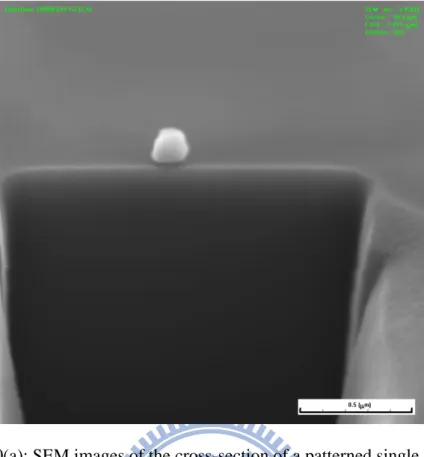
Figure 3-9(b): SEM images of the nano holes array ... 63 Figure 3-10(a): SEM images of the cross-section of a patterned single
IX
nanodiamond ... 64
Figure 3-10(b): AFM images of patterned single nanodiamond arrays ... 64
Figure 3-11(a): Raman spectra of pattern-in and pattern-out area ... 65
Figure 3-11(b): PL spectra of pattern-in and pattern-out area ... 65
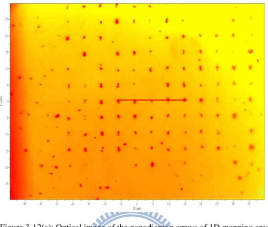
Figure 3-12(a): Optical image of the nanodiamon arrays of 1D mapping area, indicated by the straight line ... 66
Figure 3-12(b): Image of the 1D Raman intensity mapping ... 66
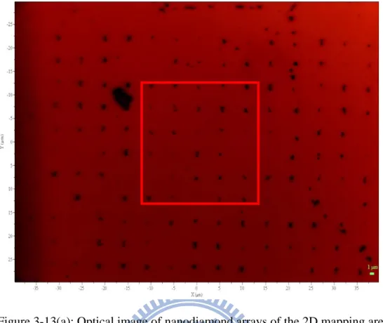
Figure 3-13(a): Optical image of nanodiamond arrays of the 2D mapping area, indicated by the square ... 67
Figure 3-13(b): Image of the 2D Raman intensity mapping ... 67
Figure 3-14(a): Optical image of the 1D mapping area, indicated by the straight line... 68
Figure 3-14(b): Image of the 2D PL intensity mapping. ... 68
Figure 3-15: IR spectra of three different samples (a) cND (b) lysozyme and (c) cND-lysozyme chip ... 69
Figure 3-16: Raman spectra of three different samples (a) lysozyme (b) lysozyme-cND complex in the solution (c) cND-lysozyme chip ... 69
Figure 3-17(a): SEM images of E.coli interaction with ND–lysozyme film on crossmark ... 70
Figure 3-17(b): SEM images of E.coli interaction with ND–lysozyme film on nanoarrays ... 70
Figure 4-1: ICG dye molecules were enhanced by metallic nanoparticles .. 86
Figure 4-2: Spectra of Healthview Nucleic Acid Stain, and ND-DNA1 and Au-DNA2 solutions were allowed to react with Healthview Nucleic Acid Stain... 86
Figure 4-3: Scheme of conjugation gold nanoparticle and nanodiamond by DNA. ... 87
Figure 4-4(a): SEM images of the hybrid structures of NDs coupled with the 13 nm gold nanoparticles, ... 87
Figure 4-4(b): SEM images of the hybrid structures of NDs coupled with the 30 nm gold nanoparticles, ... 88
Figure 4-4(c): SEM images of the hybrid structures of NDs coupled with the 50 nm gold nanoparticles, ... 88
Figure 4-4(d): SEM images of the hybrid structures of NDs coupled with the 80 nm gold nanoparticles, ... 89
Figure 4-5: SEM image of NDs interacted with gold nanoparticles without DNA ... 89 Figure 4-6: HRTEM image of a 30 nm gold nanoparticle attached on a ND
X
via a double string DNA ... 90 Figure 4-7(a): PL spectra of bare ND, gold nanoparticles, Au-DNA2
assembly, and ND-DNA1 assembly ... 90 Figure 4-7(b): Absorption spectra of 13nm, 30nm, 50nm, and 80nm Au
nanoparticles ... 91 Figure 4-8(a): Plasmon enhanced PL spectra of Au-DNA-ND hybrid
structures with gold nanoparticle sizes of 13 nm ... 91 Figure 4-8(b): Plasmon enhanced PL spectra of Au-DNA-ND hybrid
structures with gold nanoparticle sizes of 30 nm ... 92 Figure 4-8(c): Plasmon enhanced PL spectra of Au-DNA-ND hybrid
structures with gold nanoparticle sizes of 50 nm ... 92 Figure 4-8(d): Plasmon enhanced PL spectra of Au-DNA-ND hybrid
structures with gold nanoparticle sizes of 80 nm ... 93 Figure 4-9: Scheme of interaction between hybrid structures and NdeI
restriction enzyme ... 93 Figure 4-10: SEM image of hybrid structures interact with the NdeI
restriction enzyme ... 94 Figure 4-11: PL spectra of bare ND, Au-DNA-ND hybrid structures before
and after interacting with NdeI restriction enzyme ... 94 Figure 4-12: Time-resolved spectra of bare NDs, ND-DNA1 assembly, and
Au-DNA-ND hybrid structures... 95 Figure A-1: Conductivity data obtained in the temperature range 300–4.2 K
for a series of films synthesized using different nitrogen concentrations. ... 120 Figure A-3: Silicon vacancies generated by ion implantation ... 120 Figure A-3: Neutral vacancy was formed after nitrogen ion implantation.
Then annealing the neutral vacancy is converted into nitrogen vacancy. ... 121 Figure A-4: HRTEM image of the N-doped UNCD ... 122 Figure A-5: Raman spectra of UNCD and nitrogen doping UNCD ... 122 Figure A-6(a): EDS spectrum which the electron beam aims at the grain
boundaries ... 123 Figure A-6(b): EDS spectrum which the electron beam aims at the grains
... 123 Figure A-7: TEM image of the nitrogen doping UNCD after treated by
microwave plasma ... 124 Figure A-8: Raman spectra of (a) nitrogen doping UNCD and nitrogen
XI
power of 800W and total pressure of 10Torr (b) over high microwave
power and total pressure ... 124
Figure A-9(a): EDS spectrum of sample A ... 125
Figure A-9(b): EDS spectrum of sample B ... 125
Figure A-10(a): SIMS spectrum of sample A ... 126
Figure A-10(b): SIMS spectrum of sample B ... 126
Figure A-11: Photoluminescence spectra of nitrogen doping UNCD, sample A. and sample B which both treated by microwave plasma ... 127
Figure A-12 (a): SEM image of the slope generated by Focus ion beam .. 127
Figure A-12 (b): Photoluminescence intensity of Si-V traced at 738nm ... 128
Figure A-12 (c): Photoluminescence intensity of Si-V traced between 550nm and 650nm... 128
1
Chapter 1 Introduction and Background
1-1 Diamond
The diamond crystal is formed by SP3-bonding structured carbon atoms. There are
two face-centered cubic lattices in the diamond lattice shifted by a vector (a/4, a/4,
a/4). The lattice parameter a is 3.56683Å . Diamond has the greatest number density,
i.e. atoms per unit volume, of any known substance. This combined with the strength
of the carbon-carbon bond, giving rise to an extraordinarily high bond energy density.
Therefore, diamond exhibits extremely mechanical properties. Diamond is known as
the hardest natural materials scoring 10 on old Mohs scale of mineral hardness [1.1].
The high bonding energy density also leads to good chemical stability for resisting
most acid and alkalis. Unlike most electrical insulators, pure diamond shows good
thermal conductivity which can reach up to 20W/cm-K at room temperature [1.2].
The thermal conductivity of pure diamond which is roughly four times more higher
than copper is the highest of any known solid and excellent insulator with
conductivity about 1015 Ω-cm [1.3]. Diamond can also be treated as semiconductor
with a wide band gap of 5.45eV. Due to the wide band gap, diamond has high optical
transmissivity around >95% form deep UV to far IR. The wide band gap grants
2
electrons from its surface with very little applied voltage.
1-2 Synthesize of diamond
1-2-1 HTHP (high temperature and high pressure) diamond
In 1954, Hall and his co-workers in General Electric (GE) achieved their first
commercially successful synthesis of diamond under HPHT (high pressure and high
temperature) where diamond is a more stable form than graphite [1.4, 1.5]. Their
breakthrough was to use a belt press which was capable to produce the pressure over
10 GPa and temperature above 2000oC. Because of the large activation energy
required for breaking carbon-carbon bonds, graphite is not necessarily transformed
into diamond, even under high pressure and temperature [1.6, 1.7]. The molten iron,
nickel or cobalt which acted as solvent-catalyst was dissolved in graphite and
accelerated its conversion into diamond. In addition, the morphology of the grown
crystals is determined by the pressure and temperature. Furthermore, the growth rate
of diamond depends on the solubility of carbon on graphite-metal and metal-graphite
interface. Therefore the concerns for the features of the stable HPHT conditions were
kept to grow high-quality diamonds. The mass-production and high-quality diamond
3
1-2-2 CVD (chemical vapor deposition) diamond
In the 1950s, a domain of research performed in the Soviet Union and U.S. focused
on pyrolysis of hydrocarbon gases at the relatively low temperature at 800oC. This
low-pressure process is known as chemical vapor deposition (CVD). Since the early
1980s, this method has been the subject of intensive worldwide research. The
advantages of CVD diamond growth include the ability to produce diamond over
large areas and on various substrates, and its well control over chemical impurities.
The CVD process does not require pressure as high as HPHT.
To activate the carbon-containing precursor molecules in the CVD process, the gas
typically must reach a temperature exceeding 2000oC. To achieve this target, several
techniques can be employed, including hot filament, plasma-assisted (DC or
microwave), combustion flame, and so on activation. Because hot-filament CVD is a
simple growth method, it has been widely accepted among diamond researchers in the
early stages of research [1.8, 1.9].
The crucial fact for the growth rate and crystal quality is not only the gas
temperature, but also the gas composition, which typically use the mixture of CH4 and
H2. During the diamond growth which is under low pressure, the graphite phases are
formed on the growth surface in a certain amount which is in accordance with the
4
the diamond CVD. For keeping the diamond phase stable, the atomic hydrogen has
gotten the function to etch the graphite phases selectively. The carbon source gas must
therefore be highly diluted with hydrogen. The hydrogen atoms which are
characteristic of diamond CVD under low pressure are believed to play crucial roles
in the process.
Depending on the types of substrate, there are two principal synthesis varieties: the
growth of diamond on diamond (homoepitaxy) and on non-diamond substrate
(heteroepiyaxy). Homoepitaxy growth results in monocrystalline layers with superior
properties. However, the growth rate is slow due to the low surface chemical activity
of diamond. Additionally, the diamond substrate is expensive and limited in size. In
the growth of heteroepiyaxy, films may consist of oriented or non-oriented grains.
They contain numerous defects, like grain boundaries and amorphous carbon, but can
be grown to large sizes.
1-2-3 Detonation of explosive
The explosive detonation is the other method of diamond synthesis. The technology
was based on the detonation transformation of carbon-containing explosives with
negative oxygen balance. The product is a mixture of different kinds of carbon,
carbon black, etc; the major product among them is ultra-dispersed diamond (UDD)
5
absorption ability and high reacting capacity [1.10]. Nevertheless, it is not able to
control the production more precisely in diamond size.
1-2-4 Ultrasound cavitation
Micron-sized diamond crystals can be synthesized from a suspension of graphite,
which is in the organic liquid at atmospheric pressure and room temperature, by using
ultrasonic cavitation. The diamond yield is about 10% of the initial graphite weight.
The estimated cost of diamond produced by this method is comparable to the HPHT
method; the crystalline perfection of the product is significantly worse to the
ultrasonic synthesis. This technique requires relatively simple equipments and
procedures, however, it has only been reported by two research groups, and has no
industrial use as of 2009 [1.11]. Numerous process parameters are not yet optimized,
such as, the preparation of the initial graphite powder, the choice of ultrasonic power,
synthesis time and the solvent. However, it does leave a route for potential
improvement of the efficiency and reduction of the cost of the ultrasonic synthesis.
1-3 Impurities in diamond
Pure diamond crystal is colorless. Colored diamonds contain crystallographic
6
coloration. Intrinsic defects include vacancies, interstitials and extended structural
defects. Small foreign elements, such as nitrogen and boron, can appear as single
atoms at lattice sites, while large impurity atoms tend to form complexes with other
impurities or vacancies. Nevertheless, more than 300 optical centers due to the
element H, He, Li, B, N, NE, S, Si, P, Ti, and so on in diamond are documented
[1.12].
1-3-1 Classification of diamond
Natural diamond can be typically classified into four types, i.e. Ia, Ib. IIa and IIb,
according to the dominant type of defect present. More than 95% of natural diamonds
belong to the type Ia. There was the highest concentration of nitrogen (up to 3000
ppm) in type Ia diamond. The aggregative nitrogen present in two major structures of
which are the A-center and B-center. The A-center consists of a pair of substitutional
nitrogen atoms in nearest neighborhood, while the B-center occurs as a complex of
four substitutional nitrogen atoms surrounding a lattice vacancy. The concentration of
nitrogen which is ranging between 150 to 600 ppm is still considerable in type Ib
diamond. Nitrogen forms dominantly in single-substitutional structure. The
single-substitutional nitrogen atoms act as donor centers in diamond. The optical
absorption of type I diamonds give rise to slightly yellow color [1.13].
7
1ppm) was defined as type II diamond. The type IIa diamond refers to the purest
crystals. Boron is one of the most dominant impurities in type IIb diamond. The only
boron related defect is single substitutional acceptor with an energy level 0.37eV
above the valence band. Therefore, the type IIb diamond shows P-type conductivity at
room temperature. Optical absorption which gives type IIb diamond the characteristic
blue color was produced by ionization of the acceptors.
The CVD diamond can contain different impurities, depending on the substrate and
mixing reaction gases. This classification is not used in CVD diamond, yet, is used for
HPHT synthesis diamond. Nitrogen is the most common contamination in the HPHT
synthesis diamond. Most diamond synthesized through the growing process by HPHT
is the type Ib. If boron was added into the growth chamber to reduce the concentration
of nitrogen, the type IIb diamond can be produced. The high temperature annealing
which lead to aggregation of single-substitutional nitrogen converse type Ib into type
Ia [1.14].
1-3-2 Analysis of defects in diamond
The Raman spectrum of diamond consists of a sharp peak at 1332cm-1, while
graphite gives a rise in the boarder peaks characterized by the D-band at 1350cm-1 and
the G-band at 1580cm-1. The width of 1332cm-1 peak line reveals that how much
8
spectra of three different CVD diamond films. The quality of diamond is clearly
distinguishable. The excitation wavelength influenced the results of Raman spectra.
The figure 1-1(b) shows the different spectra of various wavelength of laser excitation
of diamond. While IR laser was used in Raman measurement, non-diamond
components emerge in the spectra due to that the IR laser is more sensitive for
SP2-bond carbon scattering. If the Raman spectra were measured by UV laser, the
fairly good quality can be obtained [1.15].
The surface morphology and structure properties also influenced the results of the
Raman spectra. In figure 1-2, Raman spectra of nanodiamonds of different size are
presented. For the size of 5-50nm nanodiamond, characteristic D-band and G-band
were dominated. For the size of 100-500nm, the intense diamond peak at 1332cm-1
exhibited with traceable graphitic or amorphous signature [1.16]. However, for the
size larger than 50nm, the structure is usually explained as diamond polycrystal
structure with graphitic structure on surface. While the nanodiamond with size 100nm
and larger, the Raman spectra have similar characters of bulk diamond which has
strong and sharp 1332cm-1 peak. For the smaller nanodiamond, the graphitic or
amorphous structure dominated the spectra. We observed that nanodiamonds with
sizes 100 nm and larger, the Raman spectra have similar characters with sharp and
9
The same difference was observed in photoluminescence spectra.
Luminescence can be excited by either an electron beam or light. The methods are
called cathodoluminescence and photoluminescence, respectively. The Raman
scattering is often measured together with photoluminescence. Additionally, electron
beam excites different optical centers at the same time, which leads to complications
in interpretation of the spectra. By contrast, selective excitation is allowed in PL by
choosing proper excitation wavelengths. Figure 1-3 (a) and (b) depicts the
photoluminescence spectra of different sizes nanodiamonds obtained by using 488
and 532 nm excitation wavelength, respectively [1.16].
Electron spin resonance (ESR) spectroscopy is a technique for studying chemical
species that have one or more unpaired electrons. Unpaired electrons in solids have a
non-vanishing spin which is associated with a magnetic moment. Consequently, the
spin states have different energies in a magnetic field. Natural and synthetic diamond
has been extensively studied by ESR, now, this method is gaining new attention due
to the possibility of using the spin states in the defect center to implement a solid state
quantum bit at room-temperature [1.17].
1-3-3 Color center of diamond
If the excited and ground states of a defect are both located within the band gap and
10
under excitation. Those defects give the crystal a characteristic color, and are thus
called color centers. A huge variety of optical color centers which maintain more than
100 different color centers can be found in diamond owing to the wide band gap of
diamond [1.18].
A very important transition occurs between the levels M=0 and n=0, it is the
zero-phonon line. In absorption, the phonon-assisted transition takes place at energies
which is higher than ZPL; in emission, however, it is at lower energies, which leads to
a mirror symmetry relative to the ZPL. In addition, the charge states are another
important property of the color centers. Generally, different charged states give rise to
the complete spectra. In the semiconductors with shallow donors and acceptors, the
equilibrium charge state of defects is determined by the position of the Fermi-level.
Nitrogen is the most prominently known impurity, which forms the nitrogen
vacancy defect in diamond and it consists of a substitution nitrogen atom with a next
nearest neighbor vacancy. According to the impurities which are close to the
surrounding area acting as electron donor or acceptor, the defects can form two types
of states: neutral nitrogen vacancy center [(N-V)0] and negative-charged nitrogen
vacancy center [(N-V)-] [1.19-1.22].
The [(N-V)-] defect in diamond which consists of a substitution nitrogen atom with
11
annealed type-Ib diamond. The resulting N-V pair has the expected C3v symmetry. It
is established that the ground state is spin triplet and the ZPL absorption corresponds
to 3A3E transition. The excited orbital doublet state produces the characteristic
zero-phonon line at 637nm (1.945 eV) with a radiative decay time of 13ns [1.23]. The
center also produces a paramagnetic resonance signal, which are the properties
confirming the C3v symmetry.
The [(N-V)0] center has nominal C3V symmetry and zero-phonon E-A optical
transition at 575nm (2.158 eV). The remarkable point of the 575nm center is the
absorption that is to be very weak to detect, especially in the case of highly nitrogen
contained type-Ib diamond. Its lifetime is 6ns at room temperature [1.24].
It has been reported that several other color centers emitting at the wavelength of
768, 746, 749, 764, 756, and 772nm was ascribed to defects containing Ni, Si and Cr
atoms [1.25-1.29]. These centers were found in diamond nanocrystals grown by CVD
method or were made in bulk diamond by ion implantation of the corresponding
species. Even the atomic structure of these centers has not been established yet.
However, the 768nm center has been tentatively ascribed to a complex containing Ni
and Si atoms: the 746, 749, 764, 756nm centers have been ascribed to Cr-related
defects, while the 772nm center night is a defect incorporating Cr and Ni atoms. A
12
luminescence lifetime of the 749nm Cr-related center is about 1 ns, which makes it
the most efficient single-photon emitter working in bulk diamond.
1-4 Application of diamond
The research efforts in diamond synthesis are rewarded by its unique properties,
which are then useful for many applications. Diamond has various advantages for
electronics in the semiconductor. Due to the band gap, it is inherently suitable to emit
or detect UV light. The low electron affinity allows electron emission at low
temperatures. Devices based on diamond work readily at harsh conditions, e.g. under
radiation or chemical corrosion. UV-sensors[1.30], light emitting diodes[1.31], cold
cathode,[1.32] metal-semiconductor FETs,[1.33] and electro-chemical electrodes[1.34]
have all, meanwhile, been implemented using diamond.
1-4-1 Nanodiamond as bio-marks
Over the past few years, nanomaterials, a branch of nano-biotechnology with
emphasis on the views of the biological, have attracted much attention [1.35]. The
study of nanomaterials involves biological applications and fabrication of
bio-functionalized devices. Quantum dots have specifically been applied in
13
owing to the quantum yield can be compared to fluorescent dyes and have less
photobleaching [1.36]. They were widely employed for the vitro imaging of
pre-labeled cells due to those advantages. The ability to image single-cell migration in
real time is expected to be important to several research areas, such as embryogenesis,
cancer metastasis, stem-cell therapeutics, and lymphocyte immunology. However, the
bio-cytotoxicity of quantum dots was concerned on medical applications. The
semiconductor quantum dots can be dissolved, in a process as known as photolysis, to
release toxic ions into the culture medium. The quantum dots must be carefully
examined before its bio-cytotoxicity can be approved for clinical use.
In comparison, nanodiamonds which consist of carbon atoms possess remarkable
features of low bio-cytotoxicity [1.37, 1.38]. As a result, the nanodiamonds is a
relative safe nanomaterials based on its non-bio-cytotoxicity and biocompatibility.
Nanodiamonds are promising nano-materials owning to good chemical stability,
various nanosizes, biocompatibility, good surface modification and good optical
property for bio-applications [1.39-1.42]. The surface of nanodiamonds can also be a
unique platform for the conjugation of chemicals and biomolecules after functional
modifications. The surface of nanodiamond can carry a variety of oxygen containing
functional groups immediately after purification in strong oxidative acids or oxidation
14
Surface carboxylated group of nanodiamond are typical ligands used for covalent
coupling of these biomolecules to nanodiamonds through amide linkage.
The Raman[1.15] and photoluminescence[1.19-1.12] properties of
nanodiamonds have been intensively studied. Some intrinsic Raman signals can be
used as detection markers or can be employed in biological objects. This diamond
Raman peak is strong and isolated, so it can be used as an indicator for allocating
nanodiamonds.
1-4-2 CVD diamond for bio-chip applications
CVD diamond can be mono- or polycrystalline. Whereas monocrystalline diamond
requires a diamond substrate, polycrystalline diamond can be grown on different
materials, such as silicon (Si) and quartz (SiO2), and is dominated by columnar
growth. For grain sizes below 500 nm, the CVD film is called nanocrystalline
diamond (NCD); after a certain thickness, the grain size near the surface exceeds 500 nm and the film then becomes microcrystalline diamond (μ-CD). In addition, a slightly different material is ultra-nanocrystalline diamond (UNCD) which the grain
size and roughness are not dependent on the film thickness, because these films do not
show columnar growth. For optimization of detection techniques and sensitivities, for
realization of highly integrated sensor arrays and for bio-interfaces, materials like Si,
15
CVD diamond is an outstanding material for bioelectronics with good electronic and
chemical properties [1.43, 1.44]. Additionally, ultra-hard diamond (50–150 GaP) is
promising with respect to mechanical stability of nanostructure.
1-4-3 Diamond for Single-photon source
The development of reliable devices for the generation of single photons is crucial
for many applications such as, for example, quantum cryptography[1.45], optical
quantum computation[1.46] as well as experiments on the foundations of quantum
optics [1.47, 1.48]. Single-photon emission was first observed from single atoms and
ions in traps and from molecules. More recently, semiconductor quantum dots and
photoactive point defects, such as nitrogen-vacancy (N-V) and silicon-vacancy (Si-V)
in diamond have been used in SPE experiments [1.49, 1.50]. Among the array of
luminescent nanomaterials, color centers in diamond seem to be the most-promising
single-photon source for quantum-physics applications, such as optics, information
processing and cryptography. This is due to the remarkable photoemission properties
of the defects, such as their extraordinary stability at room temperature and their high
quantum efficiency (typically >0.1), which are combined with the unique chemical
and mechanical properties of the diamond material itself. Moreover, the association of
a spin structure in the ground level resulted in a long coherence time at room
16
quantum-state preparation by optical pumping and single-spin quantum state readout
[1.51].
1-5 Research motivation and object
Nanodiamond carry the following features, such as, good photostability, easy
surface-modification, and low cytotoxicity to be considered as a good nanomaterial
for bio-applications. In this thesis work, we have developed a new technique which is
a combination of SAM and E-beam lithography to pattern nanodiamond on silicon
base substrate. As a result of the good bio-molecules absorptivity of nanodiamond, the
nanodiamond arrays can easily be bio-functionalized. The technique which we
demonstrated here is suitable for applications of bio-sensing chips and single
bio-molecule patterning and detection. In what follows, we will expect to develop it to
be as bio-chip based on bio-functionalozed nanodimond arrays.
The optical property of nanomaterials plays an important role for bio-applications,
such as bio-labeling or optical sensing. The surface plasma resonance effect from the
metallic nanoparticles greatly enhances the optical property. The ability to increase
the fluorescence emission can greatly improve the effectiveness of fluorescence-based
applications, such as single molecular detection and sensing in biology. The surface
17
applied as template for bio-sensing chips. This optical enhancement can be used as
optical sensing bio-sensors.
1-6 Reference
[1.1] P. G. Read, Gemmology. Butterworth-Heinemann., 49,
[1.2] L. H. Wei, P. K. Kuo, and R. L. Thomas, "Thermal Conductivity of Isotopically
Modified Single Crystal Diamond," Phys. rev. lett., vol. 70, 3764, (1993)
[1.3] A.T. Collins, "The Optical and Electronic Properties of Semiconducting
Diamond," Philos. T. R. Soc. A, vol. 342, 233, (1993)
[1.4] H. T. Hall, "Ultra-high pressure apparatus," Rev. Sci. Instr., vol. 31, 125, (1960)
[1.5] F. P. Bundy, H. T. Hall, H. M. Strong and R. H. Wentorf, "Man-made diamonds,"
Nature, vol. 176, 51, (1955)
[1.6] H. P. Bovenkerk, F. P. Bundy, H. T. Hall, H. M. Strong and R. H. Wentorf,
"Preparation of diamond," Nature, vol. 184, 1094, (1959)
[1.7] R. M. Hazen, "The diamond makers," Cambridge University Press, GE diamond,
100, (1999)
[1.8] S. Matsumoto, Y. Sato, M. Tsutsumi, and N. Setaka, "Growth of diamond
paeticles from methane-hyfrogen gas," J. Mater. Sci., vol. 17, 3106, (1982)
18
phase in microwave plasma," J. Cryst. Growth., vol. 62, 642, (1983)
[1.10] P. Decarli, and J. Jamieson, "Formation of Diamond by Explosive Shock,"
Science, vol. 133, 1821, (1961)
[1.11] E. M. Galimov et al, "Experimental Corroboration of the Synthesis of Diamond
in the Cavitation Process," Doklady Physics, vol. 49, 150, (2004)
[1.12] A. Zaitsev, ―Vibronic spectra of impurity-related optical centers in diamond,‖ Phys. Rev. B, vol. 61, 12909, (2000)
[1.13] K. Iakoubovskii, Optical Study of Defects in Diamond. PhD thesis, Catholic
University of Leuven, Belgium, (2000)
[1.14] T. Evans and Z. Qi, ―The kinetics of the aggregation of nitrogen atoms in diamond,‖ Proc. R. Soc. A, vol. 381, 159, (1982)
[1.15] J. Wagner, C. Wild, and P. Koidl, ―Resonance effects in raman scattering from polycrystalline diamond films,‖ Appl. Phys. Lett., vol. 59, 779, (1991)
[1.16] P.H. Chung, E. Perevedentseva, C.-L. Cheng a, "The particle size-dependent
photoluminescence of nanodiamonds," Sur. Sci., vol. 601, 3866, (2007)
[1.17] J. Wrachtrup and F. Jelezko, ―Processing quantum information in diamond,‖J. Phys.: Condens. Matter, vol. 18, S807, (2006)
[1.18] G. Davies, "Properties and Growth of Diamond," INSPEC, The Institution of
19
[1.19] G. Davies and M. F. Hamer, "Optical Studies of the 1.945 eV Vibronic Band in
Diamond," Proc. R. Soc. Lon. Ser.-A, vol. 348, 285, (1976)
[1.20] G. Davies, S. C. Lawson, A. T. Collins, A. Mainwood, and S. J. Sharp,
"Vacancy-related centers in diamond," Phys. Rev. B, vol. 46, 13157, (1992)
[1.21] Y. Mita, "Change of absorption spectra in type-Ib diamond with heavy neutron
irradiation," Phys. Rev. B, vol. 53, 11360, (1996)
[1.22] G. Davies, "Charge states of the vacancy in diamond," Nature, vol. 269, 498,
(1997).
[1.23] A. T. Collins, M. F. Thomaz and M. I. B. Jorge "Luminescence decay time of
the 1.945 eV centre in type Ib diamond," J. Phys. C Solid State Phys., vol. 16, 2177,
(1983)
[1.24] M. I. B. Jorge, M. E. Pereira, M. F. Thomaz, G. Davies, and A. T. Collins,
"Decay times of luminescence from brown diamonds," Port. Phys., vol. 14, 195,
(1983)
[1.25] I. Aharonvich, C. Zhou, A. Stacey, F. Treussart, J. F. Roch, and S. Prawer,
"Formation of color centers in nanodiamonds by plasma assisted diffusion of
impurities from the growth substrate," Appl. Phys. Lett., vol. 93, 243112, (2009)
[1.26] I. Aharonvich, C. Zhou, A. Stacey, J. Orwa, S. Castelletto, D. Simpson, A. D.
20
in the near infrared from a diamond color center," Phys. Rev. B, vol. 79, 235316,
(2009)
[1.27] D. Steinmetz, E. Neu, J. Meijer, W. Bolse, and C. Becher "Single photon
emitters based on Ni/Si related defects in single crystalline diamond,"
arXiv:1007.0202
[1.28] I. Aharonvich S. Castelletto, B. C. Johnson, J. C. McCallum, D. A. Simoson, A.
D. Greentree and S. Prawer. "Chromium single-photon emitters in diamond fabricated
by ion implantation," Phys. Rev. B, vol. 81, 121201, (2010)
[1.29] P. Siyushev et al "Low-temperature optical characterization of a near-infrared
single-photon emitter in nanodiamonds," New J. Phys., vol. 11, 113029, (2009)
[1.30] K. Hayashi, Y. Yokota, T. Tachibana, K. Kobashi, J. Achard, A. Gicquel, C. Olivero, M. Castex, and A. Treshchalov, ―Temporal response of UV sensors made of highly oriented diamond films by 193 and 313 nm laser pulses,‖ Diamond Relat. Mater., vol. 10, 1794, (1991)
[1.31] S. Koizumi, K. Watanabe, M. Hasegawa, and H. Kanda, ―Ultraviolet emission from a diamond pn junction,‖ Science, vol. 292, 1899, (2001)
[1.32] K. Okano, S. Koizumi, S. R. P. Silva, and G. A. J. Amaratunga, ―Lowthreshold
cold cathodes made of nitrogen-doped chemical-vapor deposited diamond,‖ Nature,
21
[1.33] H. Umezawa, K. Tsugawa, S. Yamanaka, D. Takeuchi, H. Okushi, and H. Kawarada, ―High-performance diamond metal-semiconductor field effect transistor with 1 μm gate length,‖ Jpn. J. Appl. Phys., vol. 38, 1222, (1999)
[1.34] T. N. Rao and A. Fujishima, ―Recent advances in electrochemistry of diamond,‖
Diamond Relat. Mater., vol. 9, 384, (2000)
[1.35] C. M. Niemeyer, "Nanoparticles, Proteins, and Nucleic Acids:Biotechnology
Meets Materials Science," Angew. Chem., Int. Ed., vol. 40, 4128, (2001)
[1.36] X. Michalet, F. F. Pinaud, L. A. Bentolila, M. Tsay, S. Doose, J. J. Li, G.
Sundaresan,A. M. Wu, S. S. Gambhir, S. Weiss, "Quantum Dots for Live Cells and in
vivo Imaging, Diagnostics and Beyond," Science, vol. 307, 538, (2005)
[1.37] A. M. Schrand, H. Huang, C. Carlson, J. J. Schlager, E. Osawa, S. M. Hussain,
and L. Dai, "Are Diamond Nanoparticles Cytotoxic?," J. Phys. Chem. B, vol. 111, 1,
(2007)
[1.38] S. J. Yu, M. W. Kang, H. C. Chang, K. M. Chen, and Y. C. Yu "Bright
Fluorescent Nanodiamonds: No Photobleaching and Low Cytotoxicity" J. Am. Chem.
Soc., vol. 127, 17604, (2005)
[1.39] H. Tamura, H. Zhou, K. Sugisako, Y. Yokoi, S. Takami, M. Kubo, K. Teraishi,
A. Miyamoto, "Periodic density-functional study on oxidation of diamond (100)
22
[1.40] E. Mironov, A. Koretz, E. Petrov, "Detonation synthesis ultradispersed
diamond structural properties investigation by infrared absorption," Diamond Relat.
Mater., vol. 11, 872, (2002)
[1.41] Wenmackers, S.D. Pop, K. Roodenko, V. Vermeeren, O.A. Williams, M. Daenen, O. Douheret, J. D’Haen, A. Hardy, M.K. Van Bael, K. Hinrichs, C. Cobet, M. vande Ven, M. Ameloot, K. Haenen, L. Michiels, N. Esser, P. Wanger, "Structural and
optical properties of DNA layers covalently attached to diamond surfaces," Langmuir,
vol. 24, 7269, (2008)
[1.42] P. Christiaens, V. Vermeeren, S. Wenmackers, M. Daenen, K. Haenen, M.
Nesladek, M. vande Ven, M. Ameloot, L. Michiels, P. Wanger, "EDC-mediated DNA
attachment to nanocrystalline CVD diamond films," Biosens. Bioelectron., vol. 22,
170, (2006)
[1.43] C.E. Nebel, J. Rinstein (eds) ―Thin-Film Diamond I,‖ Semiconductors and
Semimetals, 76, Elsvier Academic Press.
[1.44] C.E. Nebel, J. Rinstein (eds) ―Thin-Film Diamond II,‖ Semiconductors and
Semimetals, 76, Elsvier Academic Press.
[1.45] N. Gisin, G. Ribordy, W. Tittel, and H. Zbinden, "Quantum cryptography," Rev.
Mod. Phys., vol. 74, 145, (2002)
23
computation with linear optics" Nature, vol. 409, 46, (2001)
[1.47] C. Braig, P. Zarda, C. Kurtsiefer, and H. Weinfurter, "Experimental
demonstration of complementarity with single photons," Appl. Phys. B, vol. 76, 113,
(2003)
[1.48] T. Aichele, U. Herzog, M. Scholzm and O. Benson, "Single-photon generation
and simultaneous observation of wave and particle properties," AIP Proc., vol. 750, 35,
(2005)
[1.49] C. Kurtsiefer, S. Mayer, P. Zarda, and H. Weinfurter, ―Stable solidstate source
of single photons,‖ Phys. Rev. Lett., vol. 85, 290, (2000)
[1.50] R. Brouri, A. Beveratos, J. P. Poizat, and P. Grangier, ―Photon antibunching in the fluorescence of individual color centers in diamond,‖ Opt. Lett., vol. 25, 1294, (2000)
[1.51] P. Neumann, R. Kolesov, B. Naydenov, J. Beck1, F. Rempp, M. Steiner, V.
Jacques, G. Balasubramanian, M. L. Markham, D. J. Twitchen, S. Pezzagna, J. Meijer,
J. Twamley, F. Jelezko and J. Wrachtrup "Quantum register based on coupled electron
24
Figure 1-1(a): Raman spectra of three different CVD diamond films [1.15]
Figure 1-1(b): The different spectra of various wavelength of laser excitation of
25
Figure 1-2: Raman spectra of nanodiamonds of different size [1.16]
Figure 1-3: (a) Photoluminescence spectra of different sizes nanodiamonds obtained
26
Figure 1-3: (b) Photoluminescence spectra of different sizes nanodiamonds obtained
27
Chapter 2 Skeleton of this thesis and instrumentation
2-1 Description of the remaining chapters
This thesis is composed of two separated but closed related research works on
nanodiamonds. A short abstract of each experimental work and instrumentation
sections are given below. More details and discussion are presented in chapter 3 and 4.
Studies related to the nitrogen-doped ultrananocrystalline diamond films generated by
microwave plasma are put in the appendix attached to this thesis.
2-1-1 Protein Functionalized Nanodiamond Arrays
Nanodiamonds possess remarkable features such as low bio-cytotoxicity, good
optical property in fluorescent and Raman spectra, and good photostability for
bio-applications. In chapter 3, we devise techniques to position functionalized
nanodiamonds on self-assembled monolayer (SAMs) arrays adsorbed on silicon and
ITO substrates surface using electron beam lithography techniques. The nanodiamond
arrays were functionalized with lysozyme to target a certain bio-molecule or protein
specifically. The optical properties of the nanodiamond-protein complex arrays were
characterized by a high throughput confocal microscope. The synthesized
28
interacting with E. coli. This work is elaborated in chapter 3.
2-1-2 Plasmon-enhanced photoluminescence from bioconjugated gold
nanoparticle and nanodiamond assembly
In this part of the work, we coupled NDs with gold nanoparticles of different sizes
using two complementary DNA sequences. After hybridizing the gold nanoparticles
on the NDs, we observed the enhancement of the photoluminescence (PL) signals
originating from the nitrogen-vacancy (N-V) center of the ND. The enhancement was
attributed to the plasmon field created by the gold nanoparticles. The lineshape of the
enhanced PL spectra was also affected by the sizes of the attached nanoparticles due
to their different resonant plasma frequencies. The signal enhancement can be used as
an indexing tool for bio-sensing applications. This work is elaborated in chapter 4.
2-2 Instrumentation
2-2-1 E-beam lithography
Generally speaking , electron beam lithograph system is constructed from four
main parts ; including electron optical column、chamber、handling system、and control
29
electron. It controls the image resolution and exposing quality. Electron optical
column is generally composed of electron gun、blanking、condense lens、stigmator、
objective lens、deflector、and electron detector (figure 2-1). These accessories enable
the electron beam ejecting from electron gun to be well-controlled and expose to the
right place.
There are three common phenomena occur during the exposure of electron beam
system ; including forward scattering、back scattering、and charging effect. Each of
them can influence the quality of the e-beam exposed patterns, especially when the
pattern size is down to sub-50nm. The effect of forward and back scattering will
broaden the pitch size and produce some proximity effect. The charging effect is the
results of the electron accumulation phenomenon. These effects will blur the exposed
image and produce a poor exposure quality (figure 2-2).
2-2-2 Confocal microscopes
The principle of confocal imaging was patented in 1957 by Marvin Minsky and
aims to overcome the limitation of traditional wide filed fluorescence microscopes
[2.1]. In wide field fluorescence microscope, the entire specimen is flooded in light
from a light source. The whole specimen in the optical path was totally excited at the
same time and the fluorescence of the specimen was detected by the microscope’s
30
microscopes is to use both point-wise illumination and detection. As shown in figure
2-3, the point illumination and a pinhole were in an optically conjugate plane in front
of the detector in order to eliminate out-of-focus signals. The name confocal stems
from this configuration. As the only signals very close to the focal plane can be
detected, the image, the image's optical resolution, particularly in the sample depth
direction, is much better than that of wide-field microscopes. However, as much of
the light from sample fluorescence is blocked at the pinhole, this increased resolution
is at the cost of decreased signal intensity – so long exposures are often required.
As only one point in the sample is illuminated at a time, 2D or 3D imaging requires
scanning over a regular raster (i.e. a rectangular pattern of parallel scanning lines) in
the specimen. The achievable thickness of the focal plane is defined mostly by the
wavelength of the used light divided by the numerical aperture of the objective lens,
but also by the optical properties of the specimen. The thin optical sectioning possible
makes these types of microscopes particularly good at 3D imaging and surface
profiling of samples.
2-2-3 Raman spectrum
Although the inelastic scattering of light was predicted by Adolf Smekal in 1923, it
is not until 1928 that it was observed in practice. The Raman effect was named after
31
means of sunlight (1928, together with K. S. Krishnan and independently by Grigory
Landsberg and Leonid Mandelstam). Raman won the Nobel Prize in Physics in 1930
for this discovery accomplished using sunlight, a narrow band photographic filter to
create monochromatic light and a "crossed" filter to block this monochromatic light.
He found that light of changed frequency passed through the "crossed" filter.
Systematic pioneering theory of the Raman effect was developed by Czechoslovak
physicist George Placzek between 1930 and 1934. The mercury arc became the
principal light source, first with photographic detection and then with
spectrophotometric detection. At the present time, lasers are used as light sources.
The Raman effect is a light scattering phenomenon. While light of frequency V0
(usually from a laser) irradiates a sample, it can be scattered. The frequency of the
scattered light can either be at the original frequency which referred to as Rayleigh
scattering or at some shifted frequency VS = V0 Vinternal (referred at as Raman
scattering). The frequency Vinternal is an internal frequency corresponding to rotational,
vibrational, or electronic transitions. In discussing the Raman effect, some commonly
used terms need to be defined. As shown in figure 2-4, radiation scattering to the
lower frequency side (to the red) of the exciting line is call Stockes scattering. The
scattering radiation at the same frequency as the incident radiation is called Rayleigh
32
is referred to as the anti-Stokes scattering. Finally, the magnitude of this shift between
the Stokes or the anti-Stokes line and the exciting line is called the Raman shift, ΔV = ∣V0 – Vinternal ∣. The energy diagram for Stokes and anti-Stokes scattering was shown in figure 2-4.
2-2-4 Luminescence
Luminescence is the emission of light from any substance and occurs from
electronically excited states. Luminescence can be of two types: fluorescence and
phosphorescence. Phosphorescence is emission of light from triplet-excited states, in
which the electron in the excited orbital has the same spin orientation as the
ground-state electron. Transitions to the ground state are forbidden and the emission
rates are slow (103-100 s-1), so phosphorescence lifetimes are typically milliseconds to
seconds. Phosphorescence is usually not seen in fluid solutions at room temperature,
but there are many deactivation processes that compete with emission, such as
nonradiative decay and quenching processes. Fluorescence is emission light from
singlet-excited states, in which the electron in the excited orbital is paired (of opposite
sign) to the second electron in the ground-state orbital. Return to the ground state is
spin-allowed and occurs rapidly by emission of a photon. Those emission rates of
fluorescence typically are 108 s-1, so that a typical fluorescence lifetime is near 10 ns.
33
spectra vary widely and are dependent upon the chemical structure of the fluorophore
and the solvent in which it is dissolved.
A fluorophore is usually excited to some higher vibrational level of either S1 or S2.
With a few rare exceptions, molecules in condensed phases rapidly relax to the lowest
vibrational level of S1. This process, called internal conversion, is nonradiative and
takes place in 10-12 seconds or less. Return to the ground state occurs to a higher
excited vibrational ground-state level, which then quickly reaches thermal equilibrium.
An interesting consequence of emission to a higher vibrational ground state is that the
emission spectrum is typically a mirror image of the absorption spectrum of the
S0S1 transition.
Molecules in the S1 state can also undergo a spin conversion to the first triplet state,
T1. Emission from T1 is termed phosphorescence and is generally shifted to longer
wavelengths (lower energy) relative to fluorescence. Transition from the T1 to the
singlet ground state is forbidden, and as a result, the rate constants for triplet emission
are several orders of magnitude smaller than those for fluorescence. As shown in
figure 2-5, processes which occur between the absorption and emission of light are
34 2-3 Reference
[2.1] Paul Daviddovits and M. David Egger, "Scanning Laser Microscope," nature,
vol. 223, 831 (1969)
[2.2]ELS-7500EX Electron Beam Lithography System Instrument Manual, ELIONIX
Inc.
35
Figure 2-1: Overlay of electron beam system and the electron optical column of electron beam system
[2.2]
36
Figure 2-2: Illustration and simulation result of forward and back scattering effect
37
38
39
Figure 2-5: Simplified Jablonski diagram with absorbance, internal conversion,
40
Chapter 3 Application of bio-functionalized nanodiamond arrays
3-1 Literature review
3-1-1 Nanodiamond
The cytotoxicity of nano-materials has been mostly concerned while the
development of biomedical applications. Among of numerous nano-materials,
nanodiamonds possess remarkable features of low-cytotoxicity. In the previous
reports [3.1], it has been shown that nanodiamonds induce no significant cytotoxicity
in variety of cell types. Jui-I. Chao, Chia-Liang Cheng, and their coworkers has
shown that nanodiamonds are no or very low cytotoxicity for lung cells. The
cytotoxicity test of nanodiamonds in human lung cells was demonstrated (figure 3-1).
It indicates that nanodiamonds did not significantly induce the cell death. The
nanodiamonds examined in many other cells including neuronal, renal, and cervical
cells also show no cytotoxicity in those cells. As a result, nanodiamonds are relatively
safe nano-materials for further evaluation of clinical applications.
Other the low cytotoxicity, the detectable fluorescence of nanodiamonds with no
photobleaching was demonstrated in previous researches [3.2]. The figure 3-2 shows
41
(blue) excited under the same conditions. Accord to the results of photostability test,
no sign of photobleaching was found for nanodiamond even 8 hours of continuous
excitation. By contrast, the fluorescence of polystyrene nanospheres was
photobleached within 0.5 hour under the same condition.
The nanodiamonds are chemically inset, but can be surface-functionalized easily.
For the oxidative acid-treated, nanodiamonds can carry a variety of
oxygen-containing such as carboxylated group. Carboxylated nanodiamond can be
used to as a staring material to prepare other surface functionalized nanodiamond. The
figure 3-3 shows the synthetic route for functionalized nanodiamonds. It demonstrates
that the surface of nanodiamonds can be modified into kinds of functional groups [3.3,
3.4].
3-1-2 Bio-chip
The development of biochip is a major thrust of biotechnology, which encompasses
a very diverse range of research. At the same time, the semiconductor fabrication
technology has been steadily perfecting the science of micro and nano- miniaturiztion.
In recently, the combination of those two technologies has enabled biotechnology to
begin packing traditionally bulky sensing tools into smaller and smaller area named as
bio-chip. Thousands of biochemical reactions were performed at those miniaturized
42
various purposes such as disease diagnosis or detection of bio- agents.
The biochip can be typically classified into two types. One is the processing chip
and the other one is microarray chip. The processing chip, also named as Lab-on-chip
(LOC), is a device which integrates several laboratory functions on a single chip by
combination of micro-fluidics and Microelectromechanical systems (MEMs) [3.5].
For the microarray chip, the bio-molecules such as DNA, protein, or cells were
deposited on the flat substrates like glasses, silicon wafer, or polymers with the high
density and small areas. Surface chemistry is used to covalently bind the sensor
molecules to the substrate medium.
The development of biochip is multi division of research systems including
bio-molecules, chip surface modification, and signal detection. The bio-molecules
modification on surface is very important for bio-chip researches. Physical adsorption
and chemical adsorption are widely used in bio-chip. In the physical adsorption,
bio-molecules attach to substrate via Van der waals force such as hydrophobic
interaction and electrostatic attraction force. In the chemical adsorption,
bio-molecules form the covalent linking with substrate. For example, amino group of
horseradish peroxidase (HRP) reacts with carboxylated group of
16-mercaptohexadecanoic (16-MHA) forming amide bonding.
43
reference for detecting reaction of biomolecules. In the previous report, Yi Cui and his
coworkers demonstrated that the electric property of silicon nanowire was altered by
charge change of surface modified molecules. The figure 3-4 shows electric properties
of surface modified nanowire were affected by the variation of pH value [3.6].
3-2 Fabrication of bio-functionalized mamodiamond arrays by self assemble
monolayer
3-2-1 Preparation of carboxylated nanodaimond solution
The average diameter of the nanodiamond (ND) power used in our experiments is
about 100nm (General Eletric company, USA). The particle size is confirmed by SEM.
The 0.15g nanodiamond powder was treated with the 160ml 5:1 mixture of
concentrated H2SO4 and HNO3 solutions at 75 oC for 1 hour in ultrasonic bath for
dispersion and stir for 11 hours for carboxylated reaction, and extensively rinsed
several times with DI water and dry [3.7] . The sediment was then collected and dried.
The functional COOH group was formed on the ND surface followed by the standard
chemical treatment mentioned above. The surface functional carboxylated group of
nanodiamonds was checked by Fourier transform infrared and Raman spectroscopy.
44
make the dissociation of water into H+ and OH- ions. While the OH- ions absorbs on
the surface of nanodiamonds, the increasing of electric charges on nanodiamond
surface induce a coulomb repulsion force between nanoparticles. Therefore, the
clustering of nanodiamonds can be avoided. The NDs solution was prepared by
adding 0.1 g of carboxylated functionalized NDs into 100 ml of deionized water
followed by an ultrasonic bath for 60 min.
3-2-2 Fabrication of nanodiamond nanoarray by self assemble monolayer
A silicon wafer was first diced into 15 mm x 15 mm chips. A silicon oxide layer
was grown on the silicon chips with a thickness of about 400 nm by using Plasma
enhanced chemical vapor deposition (PECVD). The substrate was first cleaned with
ultrasonic bath in acetone, isopropyl alcohol, and deionized water solution for 5 min.
Then the ZEP520 photoresist was spin-coated on the silicon oxide substrates at a rate
of 500 rpm for 10 sec and 5000 rpm for 50 sec, and baked at 180 oC for 2 min. The
thickness of the photoresist on the slicon chip was about 300 nm.
Self-assembled monolayer (SAM) is an organized layer of amphiphilic molecules
in which one end of the molecules, the head group shows s specific, reversible
addinity for substrates. SAMs are created by the chemical sorption of hydrophilic
head groups onto a substrate from the vapor or liquid phase followed by a slow two
45
form either a disordered mass of molecules or form a lying down phase, and over a
period of minutes to hours, begin to form crystalline or semicrystalline structures on
the substrate surface. The hydrophilic head groups assemble together on the substrate,
while the hydrophobic tail groups assemble far from the substrate. Areas of
close-packed molecules nucleate and grow until the surface of the substrate is covered
in a single monolayer. To form an amino-terminated layer on the surface of substrate,
the substrates were immersed in 5 vol% solution of 3-aminopropyl triethoxysilane
(APTES) in 95% ethanol for 4 hours and later rinsed with ethanol and thermally
treated at 120 oC for 60 min [3.10].
The patterned substrate was dipped into 3 ml of the NDs solution and 3 ml of 0.1 M
MES buffer (2-(N-morpholino) ethane sulfonic acid). After which, 6 ml of 0.025 M
EDC solution 1-ethyl-3-[3-(dimethylamino)propyl]carbodiimide hydrochloride, 0.025
M NHS solution (N-hydroxysuccinimide) (here after ―EDC/NHS solution‖) and 8 ml
deionized water were added into the reaction and allowed to stabilize for 8 hours.
After the reaction was completed, the substrate was washed with acetone. The entire
template was then immersed into ZDMAC (dimethylacetamide) solution for 4 hours
to remove the photoresist. The substrate was again washed with acetone and
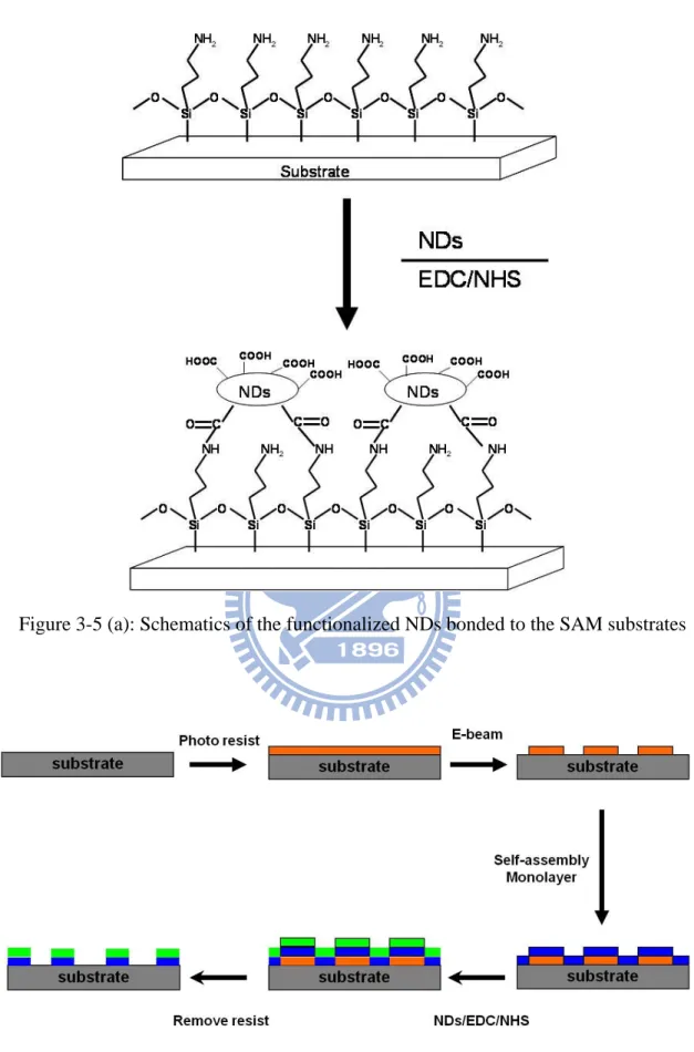
deionized water, then dried with N2. The figure 3-5 (a) and (b) show how the
![Figure 2-1: Overlay of electron beam system and the electron optical column of electron beam system [2.2]](https://thumb-ap.123doks.com/thumbv2/9libinfo/8609540.190627/48.892.233.679.123.747/figure-overlay-electron-beam-electron-optical-column-electron.webp)
![Figure 3-4: Electric properties of surface modified silicon nanowire were changed under the variation of pH value [3.6]](https://thumb-ap.123doks.com/thumbv2/9libinfo/8609540.190627/71.892.310.599.517.885/figure-electric-properties-surface-modified-silicon-nanowire-variation.webp)