A 2.4-GHz CMOS Down-Conversion Doubly Balanced Mixer
with Low Supply Voltage
Chih-Chun Tang, Wen-Shih Lu, Lan-Da Van and Wu-Shiung Feng
Lab. 328, Department of Electrical Engineering, National Taiwan University
Taipei, Taiwan, ROC
E-inail: tang1 2 [email protected]
-Image Rejectio Filter
ABSTRACT
IF DF Filter +Stage A CMOS down-conversion mixer with the combination of Gilbert Cell mixer and modified low voltage design technique using LC-tank is demonseated in tlis paper. The RF. LO and IF port frequencies are 2.4GHz. 2.3GHz and 1OOMHz. respectively. The
measurement results of the proposed mixer exhibit 6.7dB of conversion gain. -18dBm of p . 1 ~ compression point and -7.5" of lIP3 with -8dBm LO power and 1.8V supply voltage. The power consumption in mixer core is 5.94mW. This mixer was fabricated in 0.35um 1P4M CMOS process and the size is 1.5 X
1.1 mm2. It can provide 0.7& conversion gain even though 1.3V supply voltage is ut&ed
1. INTRODUCTION
In the past few years. with the growing popularity of mobile PCS.
GPS. and wireless-LAN. the wireless communication business has become a big market. The manufacturers have to integrate system in order to reduce the size. weight. and cost of the products. Many researches have explored the characteristics of CMOS in radio
frequency (RF) [1.2] such that deep sub-micron CMOS has
became an attractive candidate in the applications of low-GHz frequency range. Unfortunately. many wireless products have short stand-by h i e or too heavy for hand-held due to their large batteries. Hence. low power consumption is the key design issue of wireless portable products.
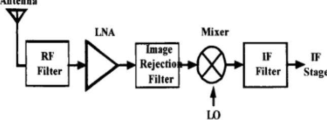
Fig. 1 shows the typical fiont-end building blocks of a
superhetrodyne receiver. Because the characteristics of image rejection 6 l t a si@cantly depend on output loading. the input impendence of RF port should match well to the output inipendence of the image rejection filter. In order to reduce the noise figure (NF) of the overall system, the mixer should have low NF and adequate conversion gain to " i z e the noise contribution of the IF stage.
On the other hand. the conversion gain should not be too large because a strong signal may saturate the output of the mixer and reduce its power gain. The input 1dB
Antenna
LNA Mixer
U)
Figure 1 The RF front-end of the superhetrodyne receiver.
IF output
power
Figure 2 The defmitions of input P-ldB. IIP3 and OlP3. compression point (P.lm) measures the input power level that causes the output power deviate from its linear niagnihide response by 1dB. Also the thircLorder inter-modulation (IM3) product
generated by two undesired adjacent channel signals characteriz~:~ another parameter of mixer linearity. called tlkcLorder intercept point (IP3). Ilie definitions of the input E l d ~ . input thir&order
intercept point (IIP3) and output thircLorder intercept point (OIF'3) are illustrated in Fig. 2. The nixer is desired to have higher linearity. so higher input P- 1 dB and LIP3 are preferred.
In terms of conversion gain. mixers can be divided into two types. which are passive and active. The advantage of the passive nuxers is better linearity, but the disadvantages are conversion loss. 1ighi:r NF and larger LO power. In contrast to the passive mixers. the active mixers provide conversion gain. lower NF and demand smaller LO power. A smaller LO power requirement is very important in mixer design. There are several reasons. First. it is M i c u l t to generate large LO power in low voltage and low power design. Second, larger LO power means larger LO-to-RF feed- through. which results in LO signal leaks through the antenna and becomes a strong interference to other RF systems. Tllird. reducing the required LO power also indicates that improve the
LO-RF and LO-IF isolation.
2.
CMOS
Mixer Design
2.1
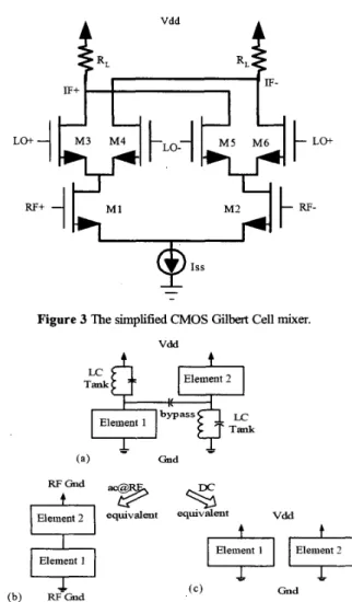
Gilbert Cell Mixer
Fig.
3 is
the conventional doubly balanced CMOSGilbert
Cellmixer [3]. The transconductance stage consists of MI and M2. and
current commutating stage consists of M3. M4. M5 and M6.
IV-794
0-7803-6685-9/01/$10.0002001
IEEE
Vdd
1 I
Figure 3 The simplified CMOS Gilbert Cell mixer.
Vdd A A Element 2
c
(a) G n d Element 2 Element 1 4 (b) WGnd=F
equivalent equivalent Vdd (C) GndFigure 4 The low voltage topology using LC tanks and bypass capacitor (a) the complete topology. (b) RF equivalent circuit. and (c) DC equivalent current.
RL
is the load resistor. The voltage gain (AV), which is given by Eq.1. is determined by the transconductance of M1.
7
L
AV
=
glllRL
-
......
...
...
.......
... ......
7r
Since all transistors operate in saturation region. the expected drain to source voltage is V~+200mV, neglecting body effect. For a typical V, of 0.W. this traditional Gilbert Cell mixer needs at least 2.7V supply voltage to operate.
2.2
Low Voltage Architecture with LC Tanks
A low voltage design technique for RF IC was proposed in [4], and Fig. 4 shows this concept. It consists of two LC tanks and one bypass capacitor. The two LC tanks resonate at the desired RF frequency to provide an infinite impendence ideally.
Figure 5 The simplified schematic of the proposed mixer. The bypass capacitor is responsible for coupling the RF signal between two branches. At DC. the LC tank requires no voltage headroom. and there is only one element between syply voltage and ground in each branch.
2.3 Proposed CMOS Mixer
The proposed CMOS mixer is shown in Fig. 5. The quality factor (Q) of on-chip spiral inductor is very low (<5) due to the CMOS lossy substrate. Assume Rs is the parasitic resistor of the inductor. the equivalent resistance of the LC tank at resonaiice. which denoted as Rr. is given by Eq. 2.
Rr
=
Rs(1
+e')
...
... ... ...
...
.(2) ASITIC [5] is used to design and simulate the on-chip inductors. If L is chosen to be 4nH. the quality factor is about 4 and the parasitic resistor is IOOhni in this 0.35~11 CMOS process. From Eq. 2. the Rr is calculated to be about 17001un. This result shows the equivalent impendence of LC tank at parallel resonance is not infinite due to the low quality factor of the on-chip inductor. If we directly apply the LC tanks to Gilbert Cell mixer. there should four LC tanks. However. the output resistance of MN3 and MN4 are abo@$.5KOhni in this circuit and much larger than 1700hm. So.MN3 and MN4 are used to replace the two LC tanks, which one is connected fiom node C to ground and the other is connected from node D to ground. Thus the mixer still works properly with smaller
chip area. The MBI and MI32 are added as buffers for
measurement to drive 5OOhnt
As compared the Gilbert Cell nkxer with the proposed mixer. the
fnst advantage of the proposed mixer is the reduction of the stacked transistors. That means it is more suitable for low voltage application than traditional Gilbm Cell mixer.
As shown in Fig. 3. the larger bias current is needed to improve the conversion gain. The larger bias current causes the larger voltage drop on RI and R2. and thus decrease the voltage headroom of the
remaining stacked MOSFETs and degrade tlie linearity of the mixer. Another advantage of the poposed nlixer is to allow the designer to easily adjust tlie bias current in the transconductance stage without affecting the current-commutating stage. This is a particular important improvement in the mixer design.
The transconductances of M1 and M 2 are set to 13mS. The overdrive voltages, (Vgs-VT), of M3 to M6 are all about 7OmV to reduce the required LO power and make sure M3 to M6 switch between saturation and cutoff region.
3.
Simulation and Measurement Results
3.1
MOSFET Model and Simulation
There are many parasitic effects in RF design and the original model provided by foundry is not accuracy enough in such high
frequency.
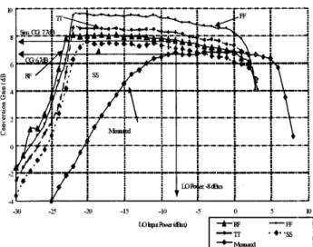
The modified MOSFET model [6] is used to simulate the circuit. The bias range of this model is 0-3V of VDS and 0-2V of V G ~ . The frequency range is from 50MHz to 20.05GHz Sweep tlie LO power from -30dBm to +3dBm to find out the conversion gain and the required LO power. The RF input signal power is set to be -47" at 2.4GHz. The conversion gain is about 7.6dB when LO power is -8dBm. To ensure the nlixer still provides the conversion gain when process deviation occurs. the other process comers are also used to simulate the same circuit. The result is shown in Fig. 6.3.2 Measurement Setup and Results
The die is mounted on FR4 board for testing. The frst step is to measure the S-parameters of the RF ports for designing the matching networks. After matching is completed. the test signal is differentially fed into RF and LO ports. The 180-degree luniped element hybrid is designed to convert the @e-aided signal to differential signal. The measured unbalance amplitude is 0.18dB at
2.3GHz and 0.16dB at 2.4GHz. Tlie phase difference is 180.3- degree at 2.3GHz and 180.5-degree at 2.4GHz. Tlie testing board is sliown in Fig. 7.
We set tlie RF power to -5OdBm and LO power to -8dBm on signal generators. Fig. 8 is the IF output frequency spectrum of the single'tone testing. The RF signal loss of cables and 180-degree hybrid is measured together to be 2.4dl3, and the loss of cable on IF port is OS&. So. the measured conversion gain is 6.7dB. After sweeping the LO power from -3OdBm to +8dBm. the conversion gain is measured and also shown in Fig. 6.
The reason of the difference in conversion gain between simulation and measurement results is the LO port does mt match to S b h m perfectly w l d e LO power is lower than - 10dBm.
LO power is set to -8dBm and perform sweep of RF power from -57.5dBm to -12.5dBm to measure the linearity of the proposed mixer. As showi in Fig. 9. the sinidation result of input P.
IdB is-19.5dB and the measurement result is-18dB. Fig. 10 shows the two tones testing result of the proposed mixer.
.M -25 -20 -15 -10 -5
u)LPt-(dto)
-7
+IvkauEd
Figure 6 The simulation and measurement results of conversion gain v.s LO power of the proposed mixer.
Figure 7 The test board of the proposed mixer.
o c l w
'b 5 L"
.
, . . I .Figure 8 The IF port output frequency spectruni of single tone testing.
The RF input tones are 2400MHz and 2401MHz and LO is 2300MHz. Thus the fundamental terms of the IF output are lOOMHz and 101MHz. The third-order inter-modulation terms are 99MHz and 102MHz. Fig. 11 shows the simulated and measured IIP3 results of the proposed mixer. The measured linearity is better than the simulation result because the measured conversion gain is slightly lower
than
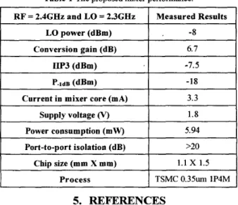
the simulation result.RF = 2.4GHz and LO = 2.3GHz LO power (dBm) Conversion gain (dB)
4.
SUMMARY
Measured Results -8 6.7 The characteristics of the proposed mixer are summarized in Table1. According to the measurement results. the proposed mixer provides 6.7dl3 conversion gain under the 1.8V supply voltage and it also demonstrates 0.7dE3 conversion gain for supply wltage as low as 1.3V. The potential for low voltage applications of the proposed mixer is proved, The proposed mixer can be easily integrated with other front-end circuits to build CMOS transceiver.
P-ldB (dBm) Current in mixer core (mA)
Figure 9 The simulated and measured results of proposed mixer. of the -18 3.3 ... .... .~ I... ... I ! Supply voltage (V) Power consumption (mw) Port-to-port isolation (dB) Chip size (mm X mm) Process .... i, ... 4 1 1 -"--7 * . I _ ,.
.
~ ' t - " " - " d $ 1 I 1.8 5.94 >20 1.1 X 1.5 TSMC 0 . 3 5 ~ 1 1P4MFigure 10 The IF port output frequency spectrum of two tones testing. -10 -20 -30 P p! -40
1
-50 !do B -70 -80 -90 -1m do -50 4 -30 -20 -10 0 R F 4 - . 1 F u n ( ~ - 3 l d 1 m n - h a h m 6 i + h hd +hhlFigure 11 The simulated and measured results of IIp3 and OIP3. Table 1 The proposed mixer performance.
IIP3 (dBmb
, I
-7.5I
5.
REFERENCES
Q. Huang. F. Piazza. P.Orsatti. and T. Ohguro "The Impact of Scaling Down to Deep Submicron on CMOS RF Circuits''
IEEE Journal of Solid-State Circuits. vol. 33, 110.7. pp.1023-
1036. July 1998.
T. Manku "Microwave CMOS-Device Physics and Design"
IEEE Joirmal of Solid-State Circuits. vol. 34. 110.3, pp277-
285. March 1999.
B. Gilbert "A precise four quadrant multiplier with subnanosecond response" IEEE Joirrnal of Solid-State
Circuits. vol. SC-3, pp.365-373. Dec. 1968.
T. Manku. G. Beck. and E. J. Shin "A Low-Voltage Design Technique for RF Integrated Circuits'' IEEE Trans. Circziifs
&wt.--Part IZ. vol. 45. no.10. pp140&1413. Oct. 1998.
A. M. Niknejad and R. G. Meyer "Analysis. Design. and Optimization of Spiral Inductors and Transfomiers for Si RF
IC's" IEEE Journal of Solid-State Circiiits. vol. 33. no.10. pp1470-1481. Oct. 1998.
C. C. Hsiao. C. W. Kuo. and Y. J. Clien "6.8GHz monolithic oscillator fabricated by 0 . 3 5 ~ 1 CMOS technologies"
Electronics Letters. vol. 36. no.23. pp. 1927-1928. Nov. 2000.