This content has been downloaded from IOPscience. Please scroll down to see the full text.
Download details:
IP Address: 140.113.38.11
This content was downloaded on 28/04/2014 at 07:40
Please note that terms and conditions apply.
Anomalous Phosphorus Cracker Temperature-Dependent Photoluminescence Spectra of
InGaP Grown by Solid Source Molecular Beam Epitaxy
View the table of contents for this issue, or go to the journal homepage for more 2000 Jpn. J. Appl. Phys. 39 L819
(http://iopscience.iop.org/1347-4065/39/8A/L819)
Jpn. J. Appl. Phys. Vol. 39 (2000) pp.L819–L821 Part 2, No. 8A, 1 August 2000
c
°2000 The Japan Society of Applied Physics
Anomalous Phosphorus Cracker Temperature-Dependent Photoluminescence Spectra
of InGaP Grown by Solid Source Molecular Beam Epitaxy
Yi-Cheng CHENG∗, Kuochou TAIand Shu-Tsun CHOU1
Institute of Electro-Optical Engineering, National Chiao-Tung University, HsinChu, Taiwan 300, Republic of China
1Compound Semiconductor Technologies Inc., Huko, Taiwan 303, Republic of China
(Received March 17, 2000; accepted for publication June 5, 2000)
InGaP grown by solid source molecular beam epitaxy showed lower effective band-gap energy with increasing phosphorus cracker temperature. Anomalous photoluminescence (PL) spectra also indicated that a weaker ordering effect was initiated when the cracker temperature was higher. Since the variation of cracker temperature mainly changed the P2/P4ratio, we believe that the more chemically reactive P2 incorporates more In into the epilayer. Therefore, InGaP grown under a more P2-rich condition has a higher In content which results in the lower band-gap energy instead of having an ordering effect.
KEYWORDS: ordering, SSMBE, photoluminescence, InGaP, valved cracker
∗E-mail address: [email protected]
L819 1. Introduction
InGaP lattice-matched to GaAs heterostructures are highly favored for application to visible light emitting devices and high-speed devices because of their large direct band gap. Both metalorganic chemical vapor deposition (MOCVD) and gas-source molecular beam epitaxy (GSMBE) have been used for the growth of high-quality InGaP layers. The high tox-icity of hydride sources, such as arsine and phosphine, used in these growth techniques, has limited their usage due to environmental concerns and expensive protection equipment. Therefore, all solid source molecular beam epitaxy (SSMBE) is preferable since it uses only solid group V sources.1)The
special components for the solid phosphorus source are a three-zone valved cracker loaded with red phosphorus,2) or a special compound cell with a GaP source.3)
In this report, using SSMBE apparatus equipped with a red phosphorus valved cracker, we studied the optical and com-positional characteristics of InGaP grown on tilted substrates at various cracker temperatures ranging from 780 to 1050◦C. The photoluminescence (PL) peak intensity and its full-width at half-maximum (FWHM) indicate that high-quality InGaP epilayers can be grown at a range of phosphorus cracker tem-peratures. However, although they are grown at much lower temperatures than that used in MOCVD, the atomic order-ing effect still appeared in the InGaP epilayers. In addition, higher In incorporation efficiency and a weaker atomic order-ing mechanism were observed at higher phosphorus cracker temperatures.
2. Experimental Details
All of the InGaP epitaxial layers were grown in a RIBER 32P system equipped with phosphorus and arsenic valved crackers. For the phosphorus cell, a 250 g 7 N red phosphorus solid rod was initially loaded into the evaporation zone. A considerable bakeout procedure was performed to remove oxygen and water vapor from the cell. Prior to the growth of phosphorus-related materials, the red phosphorus zone was heated to 380◦C for 2 hours and the white zone was main-tained at 70◦C to generate the phosphorus vapor. During the epitaxy, the arsenic cracker temperature was fixed at 920◦C and the growth temperature of GaAs was at 580◦C. The growth temperature of InGaP was then maintained around
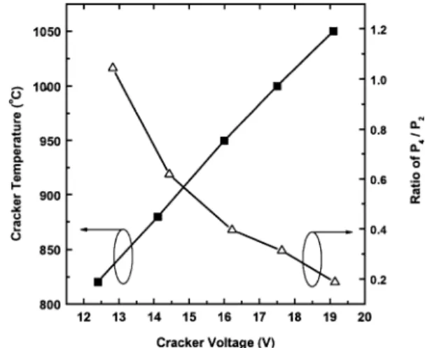
Fig. 1. P4to P2flux ratio and phosphorus cracker temperature as functions
of the voltage applied to the phosphorus cracker.
500◦C. The beam equivalent pressure (BEP) used for phos-phorus was 1.0×10⁻⁵Torr. All samples were grown at a V/III ratio of 15. The composition of InGaP epilayers was charac-terized by X-ray diffractometry (XRD) and PL spectroscopy. 3. Results and Discussion
Figure 1 shows the phosphorus cracker temperature and the P4/P2 ratio as functions of the voltage of the cracker power
supply. The dependence of the P4/P2flux ratio on phosphorus
cracker temperature was confirmed by residual gas analysis. As revealed in Fig. 1, the P4/P2ratio reduced by a factor of 5
when the phosphorus cracker temperature was changed from 820 to 1050◦C. However, the chamber pressure did not show a noticeable change when the phosphorus cracker temperature was changed; it stayed at around 1.0 × 10⁻⁵Torr. This phe-nomenon is different from the behavior observed in the case of changing the arsenic cracker temperature.4)
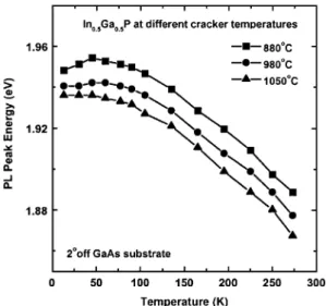
Figure 2 shows that, with exactly the same growth condi-tion and tilt angle of substrates, the PL peak energy of the InGaP samples varies with the phosphorus cracker tempera-ture in the measured temperatempera-ture range. All of the substrates tilted 2◦ off-axis from the [001] direction toward the [110] direction. It is also interesting to see that at low measur-ing temperatures from 13 to 100 K, each sample showed a different temperature-dependent variation of the PL peak en-ergy. The sample grown at a phosphorus cracker temperature of 880◦C showed a PL peak energy of ∼1.946 eV at 13 K.
The peak energy increased to∼1.952 eV at 50 K and then de-creased monotonically to lower values with further increase in measuring temperature. The sample grown at a phos-phorus cracker temperature of 980◦C showed a similar but less prominent trend. The FWHMs are 16, 13, and 11 meV for phosphorus cracker temperatures of 880, 980, and 1050◦C, respectively. The narrower FWHM indicates that the quality could be better when the cracker temperature increases. A previous study has shown that,5)at low temperatures, the epi-taxial InP layer has a negative thermal expansion coefficient that can cause an anomalous PL spectrum similar to that dis-cussed above. InGaP epilayers may possess the same negative thermal expansion coefficient at low temperatures and exhibit this anomalous luminescent feature. However, since the sam-ple grown at a cracker temperature of 1050◦C did not show the same feature at low temperatures, there is likely another effect involved.
A study of InGaP grown by MOCVD showed a similar anomalous PL spectra and the researchers attributed this phe-nomenon to the atomic ordering of related defects in the epi-layer.6) Using transmission electron diffraction, the authors
of the above-mentioned report also proved that a more promi-nent anomalous PL feature implied a stronger ordering ef-fect. The InGaP epilayer grown by SSMBE may also have the ordered structures that can cause the anomalous PL spec-tra. Therefore, the results presented in Fig. 2 indicated that the InGaP sample grown at the phosphorus cracker tempera-ture of 880◦C had the strongest ordering effect while the one grown with the phosphorus cracker temperature of 1050◦C had the weakest.
In contrast, it is widely accepted among scientists that the ordering effect should reduce the effective band gap-energy of compound semiconductors. The results revealed in Fig. 2 should therefore imply that the sample grown with the phos-phorus cracker temperature of 880◦C had the weakest or-dering effect due to its having the highest PL peak energies of the entire measuring temperature range. The contradic-tion between this argument and the one in the above seccontradic-tion prompted us to separate the two mechanisms, the ordering effect and the phosphorus cracker temperature effect, in or-Fig. 2. Temperature-dependent PL peak energies of the InGaP samples with phosphorus cracker temperatures of 880, 980 and 1050◦C, respec-tively.
Fig. 3. Room-temperature PL peak energy versus substrate tilt angle with phosphorus cracker temperatures of 880, 930 and 980◦C, respectively. der to gain further understanding of the use of phosphorus crackers in a SSMBE system. Hence, we grew more sam-ples on substrates with different tilt angles to monitor the PL peak energy shift in each sample. The use of misoriented sub-strates is a popular method to diminish the ordering effect in MOCVD. However, we used this method instead to identify the existence of the ordering effect in our samples and also used the relative PL peak energy shift measured from each of these samples to compare the relative magnitude of the effect. Three sets of GaAs substrates with different tilt angles, 0◦, 2◦, and 15◦, were used and mounted together on a 3-inch molybdenum block with high-purity indium (6N) solder. All the angles tilted from the [001] direction toward the [110] di-rection. In each growth run, a different phosphorus cracker temperature was used in order to compare the cracker temper-ature effect once again. Figure 3 shows the room-tempertemper-ature PL peak energy of the InGaP epilayers grown on substrates with different tilt angles at various phosphorus cracker tem-peratures. With the same tilt angle, the PL peak energy of the InGaP epilayer grown at a lower cracker temperature is always higher than that grown at a higher cracker tempera-ture. The largest energy difference of∼15 meV was observed from the two samples grown on the on-axis substrates with a cracker temperature of 880◦C and 980◦C. In addition, no matter how the cracker temperature changed, higher peak PL energies were always observed from the samples with larger substrate tilt angles. Since this is similar to what is observed in InGaP samples grown by MOCVD, the decrease of the PL peak energy with a lower tilt angle indicated the existence of the atomic ordering effect.
Similar to the results reported by other groups and as is evident in our results in Fig. 3, increasing the substrate tilt angle can decrease the atomic ordering effect in the SSMBE-grown InGaP epilayers. However, it remains unclear why the phosphorus cracker temperature also affected the PL peak en-ergy in our InGaP samples. As indicated in both Figs. 2 and 3, regardless of the substrate tilt angle, all samples showed a lower PL peak energy when the phosphorus cracker tempera-ture was higher. It is also worth noting that although the PL peak energy reached its highest value whenever a 15◦off-axis substrate was used, the temperature of the phosphorus cracker
still affected the PL peak energy of these samples. Accord-ing to other researchers7, 8)and our earlier study,9)the
sponta-neously initiated atomic ordering effect in the InGaP epilayer should be diminished until it becomes neglible when a sub-strate with a tilt angle as large as 15◦ was used. Under our growth condition, the ordering effect in the InGaP epilayer grown by SSMBE can apparently be suppressed by increas-ing the substrate tilt angle, but the variation of the phosphorus cracker temperature may have also affected the growth mech-anism.
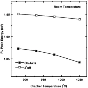
Figure 4 shows InGaP samples grown at different phos-phorus cracker temperatures on two different substrates, one the on-axis or zero tilt angle and the other the off-axis or 2◦tilt angle. It is apparent that the phosphorus cracker temperature affects the PL peak energy more when a smaller substrate tilt angle is used, although the atomic ordering effect is weaker with a larger tilt angle. Since the phosphorus cracker tem-perature mainly changes the species of phosphorus adatoms during epitaxy, we believe that the chemical reactiveness of phosphorus species plays a major role in the anomalous PL spectra shown in Fig. 2. As indicated in Fig. 1, a higher phos-phorus cracker temperature generates more P2, which is more
chemically reactive than P4. When InGaP was grown under a
more P2-rich condition, a great amount of In is incorporated
into the epilayer. According to Vegard’s law, a slight variation of In composition in InGaP can change the band-gap energy dramatically. The results shown in our experiments can be in-terpreted as an In composition variation of∼1–2%, at most.
Unfortunately, neither a double-crystal X-ray rocking curve nor transmission electron microscopy in our laboratory could provide unequivocal evidence of this small In variation. In addition, a more P2-rich condition could also reduce the
or-dering effect, as indicated by the less prominent PL feature shown in Fig. 2. More advanced calibration work is needed to fully understand this phenomenon.
4. Conclusions
In conclusion, we have observed anomalous PL spectra measured from InGaP samples grown with different substrate tilt angles and different phosphorus cracker temperatures. It is apparent that using tilted substrates could reduce the or-dering effect in InGaP grown by SSMBE, but the change of the phosphorus cracker temperature still caused prominent PL peak energy variation. While the ordering effect was weaker when a substrate with a larger tilt angle was used, the PL peak energy was lower when a higher phosphorus cracker temperature was used. Since the variation of cracker temper-ature mainly changed the P2/P4ratio, we attributed this
phe-nomenon to the chemical reactiveness of phosphorus species involved during epitaxy. Although it is not fully justified, we believe that when InGaP was grown under a more P2-rich
condition, the chemically more reactive P2could incorporate
more In into the epitaxial layer, which resulted in a lower band-gap energy, instead of increasing the ordering effect. In fact, a more P2-rich condition could have reduced the
order-ing effect, accordorder-ing to the anomalous PL spectra. Acknowledgements
The authors would like to thank Professor Kei-Feng Huang of the National Chiao-Tung University and Dr. Wen-Jen Lin and Dr. Wen-How Lan of the Chung-Shan Institute of Sci-ence and Technology for experimental assistance. This work was supported by NSC (89-2112-M-009-018) and MOEA (89-EC-2-A-17-0285-015) of Taiwan, Republic of China.
1) J. N. Baillargeon, A. Y. Cho and R. J. Fischer: J. Vac. Sci. & Technol. B13 (1995) 64.
2) G. W. Wicks, M. W. Koch, J. A. Varriano, F. G. Johnson, C. R. Wie, H. M. Kim and P. Colombo: Appl. Phys. Lett. 59 (1991) 342.
3) T. Shitara and K. Eberl: Appl. Phys. Lett. 65 (1994) 356.
4) Y. C. Shih, T. R. Block and B. G. Streetman: J. Vac. Sci. & Technol. B10 (1992) 863.
5) H.-M. Kagaya and T. Soma: Solid State Commun. 58 (1986) 479. 6) M. Kondow, S. Minagawa, Y. Inoue, T. Nishino and Y. Hamakawa: Appl.
Phys. Lett. 54 (1989) 1760.
7) A. Gomyo, T. Suzuki and S. Iijima: Phys. Rev. Lett. 60 (1988) 2645. 8) S. Minagawa and M. Kondow: Electron. Lett. 25 (1989) 758.
9) Y. C. Cheng, K. Tai, S. T. Chou, K. F. Huang and S. L. Tu: Jpn. J. Appl. Phys. 37 (1998) L200.
Fig. 4. Room-temperature PL peak energy as a function of the cracker tem-perature measured from InGaP samples grown on substrates with two dif-ferent tilt angles.