應用超臨界流體於氧化鋁閘極介電層有機薄膜電晶體之研究
74
0
0
全文
(2) 應用超臨界流體於氧化鋁閘極介電層 有機薄膜電晶體之研究 Organic Thin Film Transistors with Supercritical Fluid Treated Al2O3 Gate Dielectrics. Student:Yi-Yu Kao. 研 究 生:高 逸 侑 指導教授:劉 柏 村. 博士. Advisor:Dr. Po-Tsun Liu. 國 立 交 通 大 學 電機學院光電顯示科技產業研發碩士班 碩 士 論 文. A Thesis Submitted to College of Electrical and Computer Engineering National Chiao Tung University in partial Fulfillment of the Requirements for the Degree of Master in Industrial Technology R & D Master Program on Photonics and Display Technologies January 2008 Hsinchu, Taiwan, Republic of China. 中 華 民 國 九十七 年 ㄧ 月.
(3) 應用超臨界流體於氧化鋁閘極介電層 有機薄膜電晶體之研究 研究生:高 逸 侑. 指導教授:劉 柏 村. 博士. 國立交通大學電機學院產業研發碩士班 摘要. 在此論文裡,我們研究了高介電常數材料與薄膜電晶體在超臨界二氧化碳流 體混合水的熱處理下其電性的改變。首先,在室溫下,利用電子槍蒸鍍系統成長 極薄的氧化鋁薄膜,厚度約為 16 奈米,為了取代傳統的高溫退火製程,我們使 用了溫度約 150°C 超臨界流體混合水的技術,為了驗證超臨界流體混合水能有效 的使水分子進入到氧化鋁,進而減少薄膜的缺陷密度,我們經由紅外線光譜儀、 熱脫附常壓游離質譜儀與 X 射線光電子能譜來做材料分析,結果均顯示於氧化 鋁薄膜內氧的含量增加,而厚度為 16 奈米氧化鉿薄膜在閘極電壓 3 伏特的操作 下,其單位面積漏電流約為 3.9×10⁻⁹ A/cm2,傳導機制亦由原本未經過處理的量 子穿隧效應轉換為熱放射效應,以上主要的原因是由於氧化鋁薄膜的缺陷密度減 少。 除此之外,我們利用電子槍蒸鍍系統,在低溫下製造氧化鋁閘極介電層有機 薄膜電晶體,但不可避免地,氧化鋁薄膜在沉積過程中,由於懸鍵和晶格的錯位, 會產生電性上的缺陷,這些缺陷會使閘極漏電流增加。而如何減少這些缺陷密度 在氧化鋁閘極介電層有機薄膜電晶體的製造中是很重要的。因此,我們發現經由 超臨界流體技術的處理之後,氧化鋁閘極介電層有機薄膜電晶體有較好的元件特 性,其漏電流、臨界電壓、次臨界擺幅和場效移動率都有顯著的提升。這些改善 主要是因為超臨界流體的技術,能有效修補懸鍵,進而減少薄膜的缺陷密度。在 給予閘極定電壓與汲極定電流的元件特性劣化分析中,在超臨界超臨界二氧化碳 流體混合水的熱處理下,氧化鋁閘極介電層有機薄膜電晶體擁有較佳的可靠度。 由這些結果均顯示,藉由超臨界流體混合水的技術,能減少薄膜的缺陷密度。. i.
(4) Organic Thin Film Transistors with Supercritical Fluid Treated Al2O3 Gate Dielectrics. Student:Yi -Yu Kao. Advisor:Dr. Po-Tsun Liu. Industrial Technology R & D Master Program of Electrical and Computer Engineering College National Chiao Tung University Abstract In this study, supercritical fluids (SCF) technology is employed originally to effectively improve the properties of low-temperature-deposited metal oxide dielectric films. In this work, 16 nm ultra-thin Aluminum Oxide (Al2O3) films are fabricated by E-gun method at room temperature, and replacing the conventional high temperature annealing with supercritical fluids treatment at 150 °C. The supercritical fluids act a transporter to deliver H2O molecule into the Al2O3 films for repairing defect states. After this proposed process, the absorption peaks of Al-O-Al bonding apparently raise and the quantity of oxygen in Al2O3 film increases from FTIR and TDS measurement, individually. The leakage current density of 16 nm Al2O3 film is cut down to 3.9×10⁻⁹ A/cm2 at |Vg| = 3 V, and the conduction mechanism is transferred from quantum tunneling to thermal emission because of the significantly reducing the defects in the Al2O3 film. Supercritical fluids technology is also proposed to effectively passivate the defects in Al2O3 gate dielectric on organic thin film transistors (OTFTs) at low temperature (150 °C). After the treatment of supercritical fluids mixed with water and propyl-alcohol, the OTFT exhibited superior transfer characteristics and lower threshold voltage. The improvement in electrical characteristics can be verified due to the significant reduction of defects in Al2O3 gate dielectric on organic thin film transistors. Under bias stress and current stress, the device, which was treated with SCCO2 with co-solvent and HMDS, has smaller value of threshold voltage shift. Also, the mobility and sub-threshold swing of this device are unchanged. It indicated that this device had better reliability than others.. ii.
(5) 誌 謝. 在這兩年的碩士求學生涯期間,有太多的人需要感謝。首先,我要感謝我的 指導老師. 劉柏村博士,感謝老師在求學期間於課業及學術研究上總是不厭其煩. 地細心教導,在待人處事上教導我應有的正確態度及不斷地給我鼓勵,使得我能 夠順利的完成碩士學位,在此致上最誠摯的敬意與謝意。 此外,還要特別感謝蔡志宗學長的指導與協助,使我在實驗及論文的寫作上 能順利完成,另外還要謝謝黃震鑠學長、鄒一德學長、李逸哲學長及楊柏宇學長, 有你們的照顧與協助才能讓我獲得更多的知識。還有要感謝與我相互扶持與合作 的周誼明同學,以及一起奮鬥的林曉嫻同學、詹長龍同學及陳勝昌同學,讓我在 作實驗的時候並不會感到孤單,而且提供我許多良好的建議。同時,我也要感謝 所有的實驗室成員—竹立煒、陳思維、郭豫杰、蔡尚祐、張繼聖、鄭逸立、陳巍 方、王超駿、林威廷、黃羿霖、蘇智昱、鄧立峰及楊維哲,有你們的陪伴使我隨 時隨地身邊都充滿了歡笑與快樂。接著,由衷的感謝國家奈米元件實驗室(NDL) 及交大奈米中心提供完善的實驗設備與充足的資源。 最後,我要感謝我最敬愛的母親—吳麗卿女士。感謝母親在我的求學過程之 中給我一個良好的環境,而且一直在背後默默的支持與關懷我,讓我能夠無後顧 之憂地專心在學業上,可以不負所望的完成學業,我願將這份榮耀獻給我的母 親。此外,還要特別感謝從大學時期就一直陪伴我到現在的女朋友—朱戌文。在 我心情鬱悶的時候給我安慰與溫暖,在我快樂的時候有人與我分享,這一路上因 為有妳的陪伴,使我的生活更多彩多姿,充滿了幸福與美滿。. 高逸侑 2008 年 1 月 iii.
(6) Contents Chinese Abstract. --------------------------------------------------------------- i. English Abstract. --------------------------------------------------------------- ii. Chinese Acknowledgment Contents. --------------------------------------------------- iii. ------------------------------------------------------------------------ iv. Table Captions ---------------------------------------------------------------- vi Figure Captions Chapter 1. -------------------------------------------------------------- vii. Introduction. 1.1 Overview of Organic Thin Film Transistors ------------------------------------ 1 1.2 Operating of Organic Thin-Film Transistors ------------------------------------ 3 1.3 Background of Metal Oxide Dielectric Motivation ---------------------------- 4 1.4 Supercritical Fluid Technology ---------------------------------------------------- 4 1.5 Motivation ---------------------------------------------------------------------------- 5. Chapter 2 Fabrication and Experiment Process 2.1 Process Flow of Metal-Insulator-Silicon (MIS) Fabrication and Experiment Process -------------------------------------------------------------------------------- 7 2.2 Process Flow of Organic Thin Film Transistors Fabrication and Experiment Process ------------------------------------------------------------------------------- 8 2.3 Organic Thin Film Transistors Parameters extraction ------------------------ 9. Chapter 3. Results and Discussions. 3.1 Analysis of Material and Discussion -------------------------------------------- 11 3.1.1 Fourier Trans-form Infrared Spectroscopy (FTIR) Analysis ---------- 11 iv.
(7) 3.1.2 Thermal Desorption System – Atmospheric Pressure Ionization Mass Spectrometer (TDS-APIMS) Analysis ----------------------------------- 12 3.1.3 X-ray Photoelectron Spectroscopy (XPS) Analysis -------------------- 12 3.1.4 Auger Electron Spectroscopy (AES) Analysis -------------------------- 14 3.2 Analysis of Metal-Insulator-Silicon (MIS) Electrical Characteristics and Discussion -------------------------------------------------------------------------- 14 3.2.1 The current density-electric field (J-E) characteristics ----------------- 14 3.2.2 Conduction Mechanism ---------------------------------------------------- 15 3.2.3 The capacitance-voltage (C-V) characteristics -------------------------- 19 3.2.4 Breakdown voltage measurement and gate bias stress ----------------- 20 3.2.5 Summary --------------------------------------------------------------------- 21 3.3 Measurement of Organic Thin-Film Transistors and Discussion ------------ 22 3.3.1 The current density-electric field (J-E) characteristics of Gate Dielectrics -------------------------------------------------------------------- 22 3.3.2 The capacitance-voltage (C-V) characteristics of Gate Dielectric ---- 23 3.3.3 The Electric Characteristics of OTFTs ---------------------------------- 24 3.3.4 Instability of Organic Thin-Film Transistors during Bias Stress ----- 25 3.3.5 Instability of Organic Thin-Film Transistors during Current Stress - 25 3.3.6 Summary --------------------------------------------------------------------- 26. Chapter 4. Conclusion ------------------------------------------------------- 27. References ----------------------------------------------------------------------- 56 Vita ------------------------------------------------------------------------------ 63. v.
(8) Table Captions. Chapter 1 Table 1-1 Critical temperature and pressure for some common fluids. ------------- 29 Table 1-2 Comparison of physical properties of CO2. --------------------------------- 29. Chapter 3 Table 3-1 Summary of binding energies for ultra thin Al2O3 films Al 2p and O 1s after various post-treatments, including SCCO2-only, H2O vapor and SCCO2 with co-solvent treatment. ------------------------------------------- 53 Table 3-2 The extracted parameters from C-V curves of Al2O3 films after different treatment, measuring at 1M Hz with gate bias swing from negative voltage to positive voltage (forward). The Vfb means the flat-band voltage, and defined as C/Cmax = 50%. The change of flat-band voltage of different- treated Al2O3 films under forward and reverse swing is label as ΔV. ---------------------------------------------------------------------------- 53 Table 3-3 The extracted parameters from C-V curves of Al2O3 films after different treatment, measuring at 1M Hz with gate bias swing from negative voltage to positive voltage (forward). The Vfb means the flat-band voltage, and defined as C/Cmax = 50%. The change of flat-band voltage of Al2O3 films as gate dielectric on OTFTs after different treatment forward and reverse swing is label as ΔV. ---------------------------------- 54 Table 3-4 The parameters extractions of the devices after different treatments on E-gun deposited Al 2 O3 and PECVD deposited gate dielectrics of OTFTs.--------------------------------------------------------------------------- 54 Table 3-5 μ/μ0 and threshold voltage shift of the devices after different treatments on E-gun deposited Al2O3 and PECVD deposited gate dielectrics of OTFTs during gate-bias stress. ---------------------------------------------- 55 Table 3-6 μ/μ0 and threshold voltage shift of the devices after different treatments on E-gun deposited Al2O3 and PECVD deposited gate dielectrics of OTFTs during current stress. ------------------------------------------------- 55 vi.
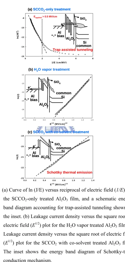
(9) Figure Captions. Chapter 1 Fig.1-1. Phase diagram for CO2. --------------------------------------------------------- 28. Fig.1-2. Density-pressure-temperature surface for pure CO2. ------------------------- 28. Chapter 2 Fig. 2-1. The supercritical fluid system. -------------------------------------------------- 30. Fig. 2-2. The experiment processes of thin Al2O3 film with various treatments. -- 31. Fig. 2-3 The experiment processes of OTFTs with various treatments. ------------- 32. Chapter 3 Fig. 3-1. The FTIR spectra of Al2O3 films. ---------------------------------------------- 33. Fig. 3-2. The transporting mechanism for SCCO2 fluids taking H2O molecule into Al2O3 film. ------------------------------------------------------------------------ 33. Fig. 3-3. The thermal desorption spectroscopy (TDS) measurement, (a) m/e (mass-to-charge ratio) = 32 peak that is attributed to O2, (b) m/e = 18 peak that is attributed to H2O. --------------------------------------------------------- 34. Fig. 3-4. The X-ray photoemission spectra of Al2O3 films Al 2p after various post-treatments, including SCCO2-only, H2O vapor and SCCO2 with co-solvent treatment. ------------------------------------------------------------- 35. Fig. 3-5. The X-ray photoemission spectra of Al2O3 films O 1s after various post-treatments, including SCCO2-only, H2O vapor and SCCO2 with co-solvent treatment. ------------------------------------------------------------- 35. Fig. 3-6. Auger electron spectroscopy: (a) SCCO2 with co-solvent treatment (b) H2O vapor treatment and (c) SCCO2-only treatment.----------------------- 36. Fig. 3-7. The leakage current densities of Al2O3 films after different treatments. (The negative bias is applied on gate electrode) ------------------------------ 37. Fig. 3-8. Conduction mechanism for Al/Al2O3/Si MIS structure. ------------------ 37. Fig. 3-9. (a) Curve of ln (J/E) versus reciprocal of electric field (1/E) for the SCCO2-only treated Al2O3 film, and a schematic energy band diagram accounting for trap-assisted tunneling shown in the inset. (b) Leakage current density versus the square root of electric field (E1/2) plot for the H2O vapor treated Al2O3 film (c) Leakage current density versus the square root vii.
(10) of electric field (E1/2) plot for the SCCO2 with co-solvent treated Al2O3 film. The inset shows the energy band diagram of Schottky-type conduction mechanism. ------------------------------------------------------------------------ 38 Fig. 3-10 The leakage current densities of Al2O3 films after different treatments (The positive bias is applied on gate electrode). Inset plots the energy band diagram of leakage current. ----------------------------------------------------- 39 Fig. 3-11 The normalized capacitance-voltage characteristics of Al2O3 films after different treatment, measuring at 1M Hz with gate bias swing from negative voltage to positive voltage (forward) and from positive voltage to negative voltage (reverse). (a) the forward swing for different treatment. The forward and reverse swing after (b) SCCO2 with co-solvent treatment (c) H2O vapor treatment and (d) SCCO 2 -only treatment. ------------------- 39 Fig. 3-12. The breakdown characteristic curves of Al2O3 films after various. treatments at negative gate bias region. --------------------------------------- 41 Fig. 3-13 The variation of leakage current of different-treated Al2O3 films as a function of stress time at a high electric field = 1.8 MV/cm. --------------- 41 Fig. 3-14 The leakage current densities of Al2O3 films as gate dielectric on OTFTs after different treatments. -------------------------------------------------------- 42 Fig. 3-15 The normalized capacitance-voltage characteristics of Al2O3 films as gate dielectric on OTFTs after different treatment, measuring at 1M Hz with gate bias swing from negative voltage to positive voltage (forward) and from positive voltage to negative voltage (reverse). ------------------------- 42 Fig. 3-16. Transfer curves of devices with different Al2O3 gate dielectrics treatment. (a) SCCO2 with co-solvent treatment (b) H2O vapor treatment ----------- 43. Fig. 3-17 (a) Drain current - gate voltage curve (ID-VG), (b) Drain current - drain voltage curve (ID-VD) and square root of Drain current - gate voltage of the device after SCCO2 with co-solvent treatment on Al2O3 gate dielectric of OTFT. ------------------------------------------------------------------------------ 44 Fig. 3-18 (a) Drain current - gate voltage curve (ID-VG), (b) Drain current - drain voltage curve (ID-VD) and square root of Drain current - gate voltage of the device after SCCO2 with co-solvent and surface (HMDS) treatment on Al2O3 gate dielectric of OTFT. ------------------------------------------------- 45 Fig. 3-19 Normalized Drain current - gate voltage curve (NID-VG) of the devices after different treatments on Al2O3 gate dielectrics of OTFTs. ------------ 46 Fig. 3-20. Atomic force microscopy analysis of Al2O3 gate dielectrics surface. (a) SCCO2 with co-solvent but without surface (HMDS) treatment, viii. (b).
(11) SCCO2 with co-solvent and surface (HMDS) treatmen --------------------- 46 Fig. 3-21 (a) Drain current - gate voltage curve (ID-VG), (b) Drain current - drain voltage curve (ID-VD) and square root of Drain current - gate voltage of the device after surface (HMDS) treatment on PECVD deposited SiNx gate dielectric of OTFT. --------------------------------------------------------------- 47 Fig. 3-22 Normalized Drain current - gate voltage curve (NID-VG) of the devices after different treatments on E-gun deposited Al2O3 and PECVD SiNx deposited gate dielectrics of OTFTs -------------------------------------------- 48 Fig. 3-23. Drain current - gate voltage curve (NID-VG) of the devices after (a) SCCO2 with co-solvent but without surface (HMDS) treatment on E-gun deposited Al2O3 and (b) SCCO2 with co-solvent and surface (HMDS) treatment on E-gun deposited Al2O3 (c) surface (HMDS) treatment on PECVD deposited SiNx gate dielectrics of OTFTs during gate-bias stress.-------------------------------------------------------------------------------- 49. Fig. 3-24 Threshold voltage shift – stress time curve of the devices after different treatments on E-gun deposited Al2O3 and PECVD deposited SiNx gate dielectrics of OTFTs during gate-bias stress.---------------------------------- 50 Fig. 3-25 Mobility ratio – stress time curve of the devices after different treatments on E-gun deposited Al2O3 and PECVD deposited SiNx gate dielectrics of OTFTs during gate-bias stress. ------------------------------------------------- 50 Fig. 3-26. Drain current - gate voltage curve (NID-VG) of the devices after (a) SCCO2 with co-solvent but without surface (HMDS) treatment on E-gun deposited Al2O3 and (b) SCCO2 with co-solvent and surface (HMDS) treatment on E-gun deposited Al2O3 (c) surface (HMDS) treatment on PECVD deposited SiNx gate dielectrics of OTFTs during current stress. --------------------------------------------------------------------------------------- 51. Fig. 3-27 Threshold voltage shift – stress time curve of the devices after different treatments on E-gun deposited Al2O3 and PECVD deposited SiNx gate dielectrics of OTFTs during current stress.------------------------------------- 52 Fig. 3-28 Mobility ratio – stress time curve of the devices after different treatments on E-gun deposited Al2O3 and PECVD deposited SiNx gate dielectrics of OTFTs during gate-bias stress. -------------------------------------------------- 52. ix.
(12) Chapter 1 Introduction 1.1 Overview of Organic Thin Film Transistor Organic thin film transistors (OTFTs) have been widely studied because they have the potential for application in low cost, large area, flexible electronics [1, 2]. OTFTs have been studied for low-cost applications, such as liquid crystal display panels, active matrix organic light-emitting diodes, sensors, postage stamps, and radio-frequency identification [3]. Low-temperature processability allows a variety of low-cost substrate materials to be used, including flexible polymeric materials [3]. Most research related to the performance of OTFTs has focused on high mobility, low operating voltage, low subthreshold swing, and a threshold voltage close to 0 V [4-7]. In particular, the high operating voltage in the range of 20–100 V is a serious obstacle for realizing practical devices. A high operating voltage not only results in high power consumption and a high cost of the driving circuit but also damages the organic materials [6]. The key technique used to solve this problem concerns the gate insulator of OTFT. In order to induce larger number of carriers at a lower voltage, the gate insulator should be thinner and its dielectric constant should be larger [6]. Therefore, high-k materials such as TiO2 and Ta2O5 should be used in order to ensure a low operating voltage and a low subthreshold swing (SS), while low-k materials such as SiO2 and SiON should be used as gate dielectrics to obtain a low leakage current and high stability. Thus, in order to ensure a low operating voltage and high stability simultaneously, Al2O3 with a dielectric constant of 8 and a low leakage current may be a good candidate as an inorganic gate insulator for OTFT devices. Although numerous studies concerning OTFT devices with inorganic gate insulators have been conducted, among them only a small number of studies have been conducted with plastic substrates. Given that the use of plastic substrates 1.
(13) requires a low-temperature deposition process, it is difficult to obtain a high-density and high-quality film for a gate insulator. To deposit a gate insulator of high-k materials on a flexible substrate, electrochemical anodization of metal thin films and electron beam evaporation have been used with low-temperature processes [6, 8, 9]. Pentacene, one of the organic semiconductors, may allow device fabrication on flexible plastic substrates. It is an aromatic compound with five condensed benzene rings and therefore, the chemical formula is C22H14 with molecular weight 278.3. The volume of the unit cell is about 705Å [10]. The permittivity is 4 [11], and the electron affinity is about 2.49eV. The optical energy gap is 2.83eV [12]. On organic small molecules, pentacene has demonstrated the highest hole and electron mobility. Pentacene has a strong tendency to form molecular crystals and when deposited by evaporation will typically form well-ordered films even for low substrate temperatures. The mobility is achieving the same range as amorphous silicon. Pentacene. transistor. drain-source. contacts. can. be. made. in. two. configurations—top contact and bottom contact. It has been demonstrated that the bottom contact configuration gives inferior performance to the top contact configuration for a range of deposition conditions and material thickness [13, 14]. As a consequence of this behavior, the top contact configuration is almost exclusively studied and reported in the literature. The surface characteristics of the gate dielectric can also play a vital role, especially for OTFTs fabricated in a “bottom-gate” architecture. This is because the surface of the dielectric strongly influences the quality of the dielectric/channel interface and the crystalline organic channel. The qualities of the interface and the organic channel, as well as the electrical properties of the gate dielectric itself, play a major role in determining the device performance of an OTFT [15]. In the present work, we have fabricated pentacene-based OTFTs using a high-k dielectric modified by two different surface treatment methods; as-prepared and hexamethyldisilasane (HMDS).. 2.
(14) 1.2 Operating of Organic Thin-Film Transistors The operation of the pentacene-based OTFT is described below [16]. Pentacene is a p-type semiconductor. At first, a negative bias is applied to the gate, the voltage drops over the insulator region and semiconductor one, which gives rise to bend the band in the semiconductor. The additional positive charges provided from the source and drain electrodes will accumulate in this region. The insulator serves as a capacitance which stores charges and can be represented as COX. It is assumed that a little voltage drop across the semiconductor is negligible. In this situation, the applied drain-bias can force the current from the source to drain. The conduction is determined by mobility μ, which represents how the electrical field drives the accumulated charges. Therefore, the increased in gate voltage δVG accounts for the increased charges COXδVG and the total charges induced over the channel are (W/L) COXδVG, where W and L correspond to the channel width and length. The increased drain current δID is then represented as. δ I D ≈ (W / L) μ COX VDδ VG. (1-1). In general, we can divide the operation of OTFTs into two regions, linear and saturation regions. At low drain voltages, the current increases linearly with drain voltage, following Ohm’s law. The drain current in the linear region is determined from the following equation I D = (W / L)COX μ (VG − VTH − VD / 2)VD. (1-2). Since the drain voltage is quite small, sometimes equation (1-2) can be simplified as I D = (W / L)COX μ (VG − VTH )VD. (1-3). For –VD > - (VG - VTH), I D tends to saturate due to the pinch-off of the accumulation layer. The current equation is modified as I D = (W / 2 L )COX μ (VG − VTH ) 2. (1-4). 3.
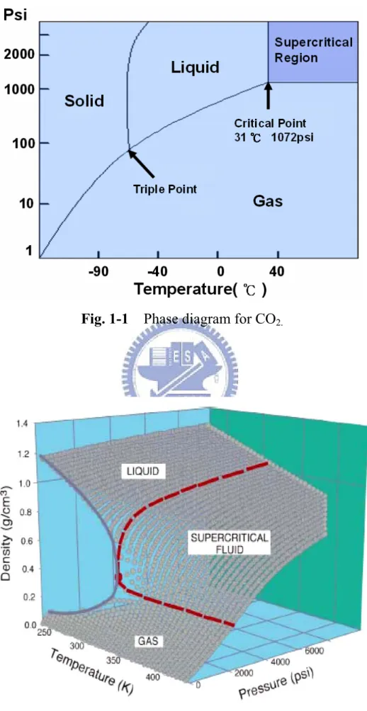
(15) 1.3 Background of Metal Oxide Dielectric (High dielectric constant material, High-k) The continuous decrease of the thickness of gate oxides used in modern electronics has to confront the limit of material itself. In order to make a breakthrough on what is aforementioned, it is necessary to increase the physical thickness as well as the dielectric constant of the gate dielectrics. The Majority of metal oxide dielectric films, such as Al2O3, Ta2O5 and HfO2, hold higher dielectric constant than oxide, and studied to replace the gate dielectric layer for future generation CMOS devices because of the lower leakage current and thicker physics thickness than thermal oxide (SiO2) under identical equivalent oxide thicknesses (EOT) [17, 18]. For thin film transistors, in pervious records, the use of low-temperature-deposited metal oxide films as gate dielectrics not only reduces the threshold voltage to near zero for pentacene and zinc oxide (ZnO2) TFTs but also the thickness of the gate insulator to nanometer scale [19, 20]. Although reduced leakage current density has been observed in some devices with high-k gate dielectrics, there are still several problems to be solved, including thermal stability, interface quality between high-k gate dielectrics and Si-substrate, mobility degradation, reliability, charge trapping, and fabrication integrity with IC technology, etc. For extending the application, the novel method to improve the quality of metal oxide films is necessary.. 1.4 Supercritical Fluid Technology The attractiveness of supercritical fluids for commercial applications is their unique combination of liquid-like and gas-like properties. Supercritical fluids are compounds above their critical temperatures and pressure, as shown in Fig 1-1 [21, 22]. The Table 1-1 shows critical temperature and pressure for some common fluids. Supercritical fluids [23-25], particularly supercritical CO2 (SCCO2), have unique. 4.
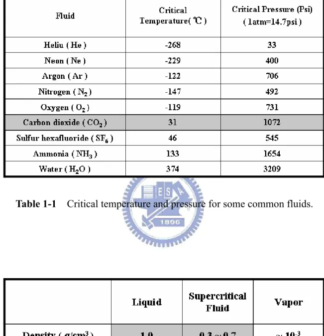
(16) characteristics and high potential in material processing [26-28]. The supercriticality is a strange and intriguing state in which solids can dissolve in gases, and liquids can alternate between reflectivity and transparency. CO2-based supercritical fluids are particularly attractive because CO2 is nontoxic, inflammable, not corrosive, not explosive, recyclable and inexpensive. Besides, its critical conditions are easily achievable with existing process equipment (31 °C, 1072 psi =72.8 atm). Figure 1-2 shows the density-pressure-temperature surface for pure CO2. It can be discovered that relatively small changes in temperature or pressure near the critical point, resulting in large changes in density. Table 1-2 shows the comparison of several physical properties of typical liquid, vapor, and supercritical fluid state for CO2. It could be seen that SCCO2 fluids possesses liquid-like density, so that SCCO2 fluids are analogous with light hydrocarbon to dissolve most solutes and own exceptional transport capability [29, 30]. On the other hand, SCCO2 fluids hold gas-like characteristic due to their viscosity and surface tension are extremely low, it allows SCCO2 fluids to keep fine diffusion capability and enter the nano-scale pores or spaces without damage. These properties are the reasons for SCCO2 fluids to employ in many commercial applications, including the extraction of caffeine from coffee, fats from foods, and essential oils from plants for using in perfumes. Furthermore, considerable attention is now paid to using SCCO2 for semiconductor processing , such. as. wafer. cleaning,. photoresist-stripping,. photoresist. drying,. and. to. manufacturing porous low-dielectric-constant thin films, by means of its high mass transfer rates and infiltration capabilities [24, 25].. 1.5 Motivation In recent records, metal oxide dielectrics, such as Al2O3, Ta2O5 and HfO2, have attracted much attention for thin film transistor liquid crystal displays (TFT-LCDs) technology on the base of glass substrates or plastics. Among several metal oxide film 5.
(17) formation methods [17, 18, 31], in general, low-temperature technology is welcome due to a low thermal budget process. However, the low-temperature-deposited dielectric films perform inferior properties and larger current leakage due to numerous traps inside the metal oxide film [32]. It is thereby required for the low-temperature-deposited metal oxide film to reduce electrical traps by implementing a post-treatment process. High-temperature (>600 °C) annealing is typically used to diminish the traps in metal-oxide films [33-34]. Nevertheless, there are several considerable issues present for high-temperature annealing process. For example, crystallizing phenomenon would occur possibly during the process duration, and leads to unexpected leakage current through grain boundaries [34-36]. Additionally, the high-temperature process is not applicable to the substrates with low glass transition temperature (Tg), such as glasses and plastics [37]. By the liquid-like property, it is allowed for supercritical fluids to own fine transport capability [38]. Supercritical fluids, in addition, hold gas-like and high-pressure properties to efficiently diffuse into thin films with no damage. Here, these advantages would be adequately employed to passivate the defects in low- temperature-deposited metal oxide dielectric film at 150 °C. Besides, OTFTs will be used in the flexible displays. The excellent transfer characteristics are thereby demanded, such as high mobility and lower threshold voltage. Especially, in recent years, the fabrication of OTFTs tends to being implemented at low temperature processes for cost down and comparable with plastic substrates (120~250 °C)[39, 40]. The performance of low-temperature-fabricated OTFTs, however, is unsuitable for application to display technology, due to the poor gate dielectrics with plenty of defects [41]. For improving electrical characteristics of OTFTs, it is necessary to passivate the defect-states in the gate dielectrics. Therefore, it is critical to develop a traps passivation technology at low temperature for extending the application of OTFTs. In this work, therefore, the supercritical fluids treatment is also proposed to effectively decrease the defects in the gate dielectrics of OTFTs at low temperature. 6.
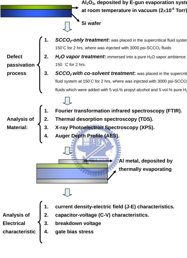
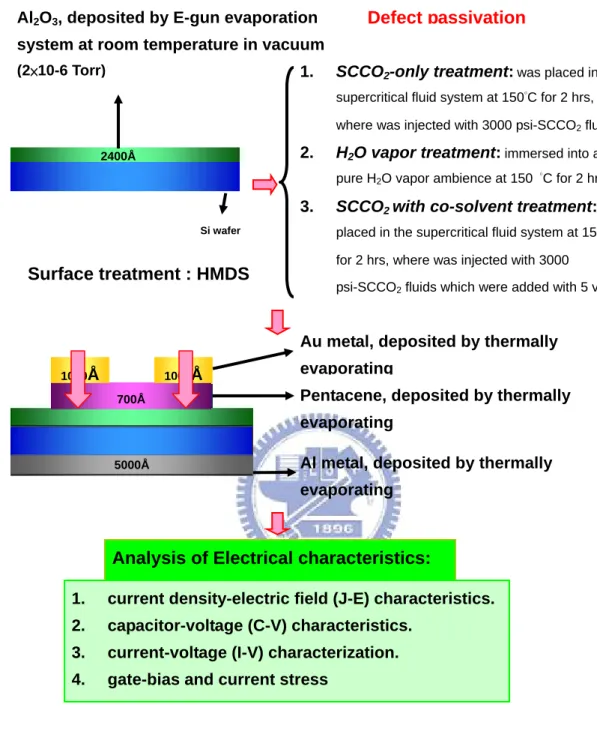
(18) Chapter 2 Application of Supercritical Fluid Technology on Metal-Oxide Dielectric Thin Film 2.1 Process Flow of Metal-Insulator-Silicon (MIS) Fabrication and Experiment Process In this experiment, a metal-oxide Al2O3 film layer was deposited on p-type (100) silicon wafers by E-gun evaporation deposition at room temperature. The thickness of as-deposited Al2O3 films was 16nm, which was measured by an ellipsometer system. Subsequently, the wafers with 16nm-thick Al2O3 film were split into three groups, and processed. with. different. post-treatments. to. study. the. properties. of. low-temperature-deposited Al2O3 film. The first group labeled as SCCO2-only treatment, was designed as the control sample, and was only treated with 3000psiSCCO2 that without co-solvent at 150 °C for 2 hrs. The second group labeled as H2O vapor treatment, was immersed into a pure H2O vapor ambience at 150 °C for 2 hrs in a pressure-proof stainless steel chamber with a volume of 100 cm3. The third group marked as SCCO2 with co-solvent treatment, was placed in the supercritical fluid system at 150°C for 2 hrs, where was injected with 3000psi of SCCO2 fluids mixed with 5 vol.% of propyl alcohol and 5 vol.% of pure H2O. The propyl alcohol plays a role of surfactant between nopolar-SCCO2 fluids and polar-H2O molecules, so that the H2O molecule uniformly distributes in SCCO2 fluids and be delivered into the Al2O3 film for passivating defects. The supercritical fluid system is shown in Fig. 2-1. After these different treatments, fourier transformation infrared spectroscopy (FTIR) and thermal desorption spectroscopy (TDS) were also used to investigate the evolution of chemical functional bonding and the content of oxygen in Al2O3 films, respectively.. Electrical. measurements. were 7. conducted. on. metal. insulator.
(19) semiconductor (MIS) capacitors by thermally evaporating Al electrodes on the front surface of the Al2O3 films and the backside of the silicon wafer. The current density-electric field (J-E) characteristics, capacitance-voltage (C-V) characteristics, breakdown voltage and gate bias stress were measured with HP4156C semiconductor parameter analyzer for investigating the transformation of Al2O3 film. The experiment processes of thin HfO2 film with various treatments are exhibited in Fig. 2-2.. 2.2 Process Flow of Organic Thin Film Transistors Fabrication and Experiment Process At second experiment, a metal-oxide Al2O3 film layer was deposited on p-type (100) silicon wafers by E-gun evaporating system at room temperature. The thickness of as-deposited Al2O3 films was 240nm, which was measured by an ellipsometer system. Subsequently, the wafers with 240nm-thick Al2O3 film were split into three groups, and processed with different post-treatments to study the properties of low-temperature-deposited Al2O3 film. The first group labeled as SCCO2-only treatment, was designed as the control sample, and was only treated with 3000psiSCCO2 that without co-solvent at 150 °C for 2 hrs. The second group labeled as H2O vapor treatment, was immersed into a pure H2O vapor ambience at 150 °C for 2 hrs in a pressure-proof stainless steel chamber with a volume of 100 cm3. The third sample marked as SCCO2 with co-solvent treatment, was placed in the supercritical fluid system at 150°C for 2 hrs, where was injected with 3000psi of SCCO2 fluids mixed with 5 vol.% of propyl alcohol and 5 vol.% of pure H2O. The propyl alcohol plays a role of surfactant between nopolar-SCCO2 fluids and polar-H2O molecules, so that the H2O molecule uniformly distributes in SCCO2 fluids and be delivered into the Al2O3 film for passivating defects. After these different treatments, the gate contact by thermally evaporating Al electrodes on the backside surface of the silicon wafer. Then, the samples were put 8.
(20) into the oven with HMDS steam for 20mins at 150 °C. Pentacene was used as an active layer. This was deposited using ULVAC thermal evaporator. The deposition is started at a pressure lower than 3×10⁻⁶ torr. The deposition rate is controlled at 0.1Å/s. The temperature we use in depositing pentacene films is 70℃. We use shadow mask to define the active region of each device. The resulting thickness of the pentacene thin film was 70 nm, which was measured by a quartz-crystal thin film thickness monitor. After pentacene deposition, we use shadow mask to define top contact of each device. The top electrodes are Au. We deposited the Au (100nm) via the thermal evaporator as the source and drain electrode pad. The deposition pressure was at 3×10⁻⁶ torr with the deposition rate of 0.5Å/sec. In addition, we fabricated the same process to comparison with insulation of SiNx by Plasma Enhanced Chemical Vapor Deposition (PECVD). After fabrication OTFTs, The current density-electric field (J-E) characteristics, capacitance-voltage (C-V) characteristics, Current-Voltage (I-V) characteristics, gate-bias stress and current stress were measured with HP4156C semiconductor parameter analyzer for investigating the OTFTs. The experiment processes of OTFTs with various treatments are exhibited in Fig. 2-3.. 2.3 Organic Thin Film Transistors Parameters extraction In this section, the methods of extraction the mobility, the threshold voltage, the on/off current ratio and the sub-threshold swing is characterized, respectively. Mobility Generally, mobility can be extracted from the transconductancein gm the linear region: ⎡ ∂I ⎤ WCO X = gm = ⎢ D ⎥ μVD L ⎣ ∂VG ⎦VD =CONSTANT. (2-1). Mobility can also be extracted from the slope of the curve of the square-root of 9.
(21) drain current versus gate voltage in the saturation region, i.e. For –VD > - (VG - VTH) :. ID =. W μCOX (VG − VTH ) 2L. (2-2). Threshold voltage Threshold voltage is related to the operation voltage and the power consumptions of an OTFT. We extract the threshold voltage from equation (2-2), the intersection point of the square-root of drain current versus gate voltage when the device is in the saturation mode operation. On/Off current ratio Devices with high on/off current ratio represent large turn-on current and small off current. It determines the gray-level switching of the displays. High on/off current ratio means there are enough turn-on current to drive the pixel and sufficiently low off current to keep in low power consumption. Sub-threshold Slope Sub-threshold swing is also important characteristics for device application. Its is a measure of how rapidly the device switches from the off state to the on state in the region of exponential current increase. Moreover, the sub-threshold swing also represents the interface quality and the defect density [42].. , when VG < VT for p-type.. (2-3). If we want to have good performance TFTs, we need to lower sub-threshold swing of transistors.. 10.
(22) Chapter 3 Results and Discussions 3.1 Analysis of Material and Discussion 3.1.1 Fourier Trans-form Infrared Spectroscopy (FTIR) Analysis. Figure 3-1 shows the FTIR spectra of Al2O3 films after various post-treatments, including SCCO2-only, H2O vapor and SCCO2 with co-solvent treatment. The functional group referred to Al-O-Al bonding is at 476 cm-1 and 600 cm-1, and the absorption peak at around 1080 cm-1 attributes to the Al-O-H bond [43, 44]. The peak intensity of Si-O-Si bond for different treatments is not obtained, meaning that these post-treatments would not make influence on the thickness and quality of the interfacial SiOx film. For the H2O-vapor-treated Al2O3 film, however, the peak intensity of Al-O-Al bands (476 cm-1 and 600 cm-1) raises apparently in comparison with the SCCO2-only-treated Al2O3 film. This is believed well that the H2O vapor would permeate into Al2O3 film and makes reaction with Al dangling bonds (i.e. traps) forming Al-O-Al bands. These traps in the low-temperature deposited Al2O3 film could be thereby passivated by H2O vapor molecules. By the way, the band at 1080 cm-1 is due to Al-O-H bending vibration o bridge hydroxyl anions. The broad intensity peak centered at approximately 3400 cm-1 is typical of O-H vibration from adsorbed water molecules [45]. Furthermore, with SCCO2 with co-solvent treatment, obvious increase in the intensity of Al-O-Al bonding is observed in the FTIR. It indicates that the H2O molecules into Al2O3 film is achieved by the SCCO2 fluids, potentially modifying the dielectric properties of Al2O3 film, and the transporting mechanism for SCCO2 fluids taking H2O molecule into Al2O3 film is shown in Fig. 3-2. 11.
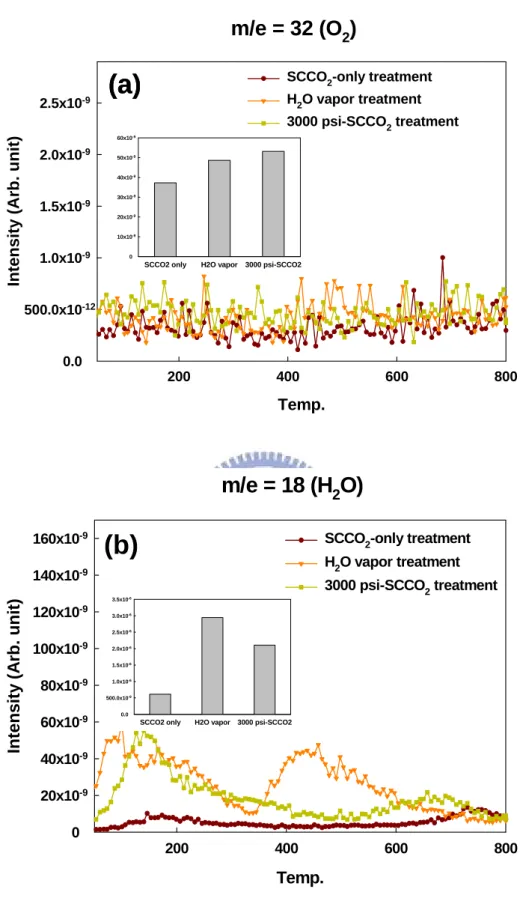
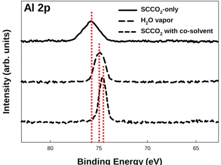
(23) 3.1.2 Thermal Desorption System – Atmospheric Pressure Ionization Mass Spectrometer (TDS-APIMS) Analysis. The TDS measurement, as shown in the Fig. 3-3, was carried out upon heating these treated Al2O3 films from 50 to 800 °C at a heating rate of 10 °C/min in vacuum (10−5 Pa.). In Fig. 3-3 (a), m/e (mass-to-charge ratio) = 32 peak that is attributed to O2 was monitored to evaluate the content of oxygen outgassing form Al2O3 films. It is clearly found the highest oxygen content is detected in the SCCO2 with co-solvent treated Al2O3 film, certainly consistent with the FTIR observation. From Fig. 3-3 (b), m/e (mass-to- charge ratio) = 18 peak that is attributed to H2O, the residual moisture in Al2O3 film is much more after H2O vapor treatment. This is result from SCCO2 fluid not only employed to transport the H2O molecule into Al2O3 film but a suitable method to remove H2O molecule in addition [46, 47].. 3.1.3 X-ray Photoelectron Spectroscopy (XPS) Analysis. XPS involves measuring the photoelectron spectra obtained when a sample surface is irradiated with x-rays. The kinetic energy (peak position) of the photoelectrons can be written as E K = hν -E B -φs -qφ where hν is the x-ray energy, EB is the binding energy (the difference between the Fermi level and the energy level being measured), φs is the work function of the electron spectrometer, q is the electronic charge, and φ is the surface potential. We have also performed XPS measurements using an Mg Kα X-ray source (1253.6 eV photons) to determine the bonding environments of the Al and O atoms. Figure 3-4 shows the XPS spectra for Al 2p level that was calibrated from C 1s peak 12.
(24) at 284.5 eV. Each spectrum was represented the result at different post-treatments, including SCCO2-only, H2O vapor and SCCO2 with co-solvent treatment. As shown in Figure 3-4 , the Al 2p peak, which has binding energy of 75.8 eV, related to Al-O bonding in Al2O3. However, the binding energy of Al 2p peak shown in Figure 3-4 varied from 75.8 eV for SCCO2-only sample to 74.7 eV [48] for SCCO2 with co-solvent treatment sample. The origins of binding energy shift (ΔBE) are suggested as a number of factors such as charge transfer effect, presence of electric field, environmental charge density, and hybridization. Among these, charge transfer is regarded as a dominant mechanism causing a binding energy shift. According to the charge transfer mechanism, removing an electron from the valence orbital generates the increment in core electron’s potential and finally leads a chemical binding energy shift [49]. Therefore, it is considered that the Al 2p peak shift originated from the enhanced charge transfer with different post-treatments, i.e., the larger portion of Al atoms was fully oxidized with SCCO2 with co-solvent treatment. Figure 3-5 shows the O 1s core level peaks also demonstrated binding energy shift with changing of different post-treatments. For the H2O-vapor-treated Al2O3 film, however, the peak intensity of Al-O bands raises apparently in comparison with the SCCO2-only treated Al2O3 film. This is believed well that the H2O vapor would permeate into Al2O3 film and makes reaction with Al dangling bonds (i.e. traps) forming Al-O bands. These traps in the low-temperature deposited Al2O3 film could be thereby passivated by H2O vapor molecules. Furthermore, with SCCO2 with co-solvent treatment, obvious increase in the intensity of Al-O bonding is observed in the XPS. It indicates that the best transport efficiency of H2O molecules into Al2O3 film is achieved by the SCCO2 fluids, potentially modifying the dielectric properties of Al2O3 film, and the transporting mechanism for SCCO2 fluids taking H2O molecule into Al2O3 film is shown in Fig. 3-2. Summary of binding energies for Al2O3 films are shown in Table 3-1.. 13.
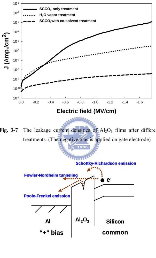
(25) 3.1.4 Auger Electron Spectroscopy (AES) Analysis. In order to analyze the composition of the Al2O3 film after various post-treatments, including SCCO2-only, H2O vapor and SCCO2 with co-solvent treatment, we performed the Auger electron spectroscopy analysis. The first group labeled as SCCO2-only treatment, was designed as the control sample, and was only treated with 3000psi-SCCO2 that without co-solvent at 150 °C for 2 hrs. The second group labeled as H2O vapor treatment, was immersed into a pure H2O vapor ambience at 150 °C for 2 hrs in a pressure-proof stainless steel chamber with a volume of 100 cm3. The third group marked as SCCO2 with co-solvent treatment, was placed in the supercritical fluid system at 150°C for 2 hrs, where was injected with 3000psi of SCCO2 fluids mixed with 5 vol.% of propyl alcohol and 5 vol.% of pure H2O. As shown in Figure 3-6, the SCCO2-only treated and H2O vapor treated films have oxygen composition lower than that of the Al2O3 film after SCCO2 with co-solvent treatment. The propyl alcohol plays a role of surfactant between nopolar-SCCO2 fluids and polar-H2O molecules, so that the H2O molecule uniformly distributes in SCCO2 fluids and be delivered into the Al2O3 film for passivating defects.. 3.2 Analysis of Metal-Insulator-Silicon (MIS) Electrical Characteristics and Discussion 3.2.1 The current density-electric field (J-E) characteristics. The leakage current densities of Al2O3 films after different treatments are shown as a function of applied negative gate bias voltage in Fig. 3-7. Among various post-treatments, the SCCO2-treated Al2O3 film exhibits the most serious leakage current, inferentially due to its poor dielectric characteristics with numerous traps inside the Al2O3 film and the interface between parasitical SiOx and Si wafer. The improvement of electrical characteristics is observed by using H2O vapor process, 14.
(26) however, a high leakage current density still appears at larger applied voltages. It could be inferred reasonably dependent on the defect passivation efficiency. The most indicating that H2O vapor can passivate the traps (or defects) and alter dielectric properties of the low-temperature-deposited Al2O3 film. After H2O vapor treatment, effective improvement of electrical characteristic is obtained by the SCCO2 with co-solvent treatment, exhibiting the lowest leakage current density among all samples. Low leakage current density (~3.9×10⁻⁹ A/cm2) is kept constantly, even biased at an electric field of 1.7 MV/cm. The electrical performance agrees with XPS analysis, in which SCCO2 with co-solvent treatment modified Al2O3 dielectrics even effectively.. 3.2.2 Conduction Mechanism. There may be different conduction mechanisms in the insulator thin film, including Schottky-Richardson emission [50], Frenkel-Poole emission [50,51], Fowler-Nordheim tunneling [50,51], and trap assisted tunneling [52,53] illustrated in Fig 3-8. The Schottky-Richardson emission generated by the thermal ionic effect is caused by the electron transport across the potential energy barrier via field-assisted lowering at a metal-insulator interface. The leakage current governed by the Schottky-Richardson emission is as following:. (. J SR = A*T 2 exp βSR E. where βSR = ( q 3 4πε 0ε ). 1. 2. 1. 2. − φSR k BT. ). , q is the electronic charge, A* is the effective. Richardson constant, φSR is the contact potential barrier, E is the applied electric field, ε 0 is the permittivity in vacuum, ε is the high frequency relative dielectric constant, T is the absolute temperature, and k B is the Boltzmann constant. We can find the slope of the leakage current equation.. ln J SR = β SR E. 1. 2. k BT + ⎡⎣ln ( A*T 2 ) − φSR k BT ⎤⎦. 15.
(27) Solpe = β SR k BT The Frenkel-Poole emission is due to field-enhanced thermal excitation of trapped electrons in the insulator into the conduction band. The leakage current equation is:. (. J FP = J 0 exp β FP E. where J 0 = σ 0 E. 1. 2. − φFP k BT. ). is the low-field current density, σ 0 is the low-field. conductivity, β FP = ( q3 πε 0ε ) 2 , q is the electronic charge, φFP is the contact 1. potential barrier, E is the applied electric field, ε 0 is the permittivity in vacuum, ε is the high frequency relative dielectric constant, T is the absolute temperature, and k B is the Boltzmann constant. We can find the slope of the leakage current equation. ln J FP = β FP E. 1. 2. k BT + ⎡⎣ln ( J 0 ) − φFP k BT ⎤⎦. Solpe = β FP k BT The Fowler-Nordheim tunneling is the flow of electrons through a triangular potential barrier. Tunneling is a quantum mechanical process similar to throwing a ball against a wall often results that the ball goes through the wall without damaging the wall or the ball. It also loses no energy during the tunnel event. The probability of this event happening, however, is extremely low, but an electron incident on a barrier typically several nm thick has a high probability of transmission. The Fowler-Nordheim tunneling current I FN is given by the expression [54]:. I FN = A G A FNε ox2 exp ( − BFN ε ox ) where the A G is the gate area, ε ox is the oxide electric field, and A FN and BFN are usually considered to be constant. A FN and BFN are given as the following:. A FN = q3 ( m mox ) 8π hΦ B = 1.54 ×10⁻⁶ ( m mox ) Φ B BFN = 8π ( 2mox Φ 3B ). 1. 2. 3eh = 6.83 ×10⁷ ⎡⎣( m mox ) Φ3B ⎤⎦. 16. 1. 2.
(28) where mox is the effective electron mass in the oxide, m is the free electron mass, q is the electronic charge, and Φ B is the barrier height at the silicon-oxide interface given in units of eV in the expression for BFN . Φ B is actually an effective barrier height that take into account barrier height lowering and quantization of electrons at the semiconductor surface. Rearranging I FN formula gives by: ln ( I FN AG ε ox2 ) = ln ( J FN ε ox2 ) = ln ( AFN ) − BFN ε ox. A plot of ln ( J FN ε ox2 ) versus. (1 ε ) ox. should be a straight line if the. conduction through the oxide is pure Fowler-Nordheim conduction [54]. In the trap assisted tunneling model, it is assumed that electrons first tunnel through the SiOX interfacial layer (direct-tunneling). Then, electrons tunnel through traps located below the conduction band of the high-k thin film and leak to substrate finally [52]. The equation of leakage current density is [53]:. J = α E ox exp ( − β E ox ) From the equations as shown above, leakage current behaviors of insulate films can be investigated further on the leakage current density J electric field E characteristics such as J vs. E. 1. 2. plots.. The plot of the nature log of leakage current density versus the square root of the applied electric field was observed. It is found that the leakage current density is linearly related to square root of the applied electric field. The linear variations of the current correspond either to Schottky-Richardson emission or to Frenkel-Poole conduction mechanism. For trap states with coulomb potentials, the expression is virtually identical to that of the Schottky-Richardson emission. The barrier height, however, is the depth of the trap potential well, and the quantity β FP is larger than in the case of Schottky-Richardson emission by a factor of 2. Leakage conduction mechanism is also investigated to support the comments on the electrical improvement of Al2O3 film. Fig. 3-9(a) plots ln (J/E) versus reciprocal of electric field variation for the SCCO2-only treated Al2O3 film, and a schematic 17.
(29) energy band diagram accounting for leakage transport mechanism shown in the inset. A good linear fitting explains Fowler-Nordheim (F-N) tunneling [55] occurs in the electric fields higher than 0.5 MV/cm. Also, it is consistent with the electrical behavior of SCCO2-only treated Al2O3 film in Fig. 3-9 that leakage current density sharply increases, while gate bias voltage larger than 0.5 MV/cm. This could be attributed to the trap-assisted tunneling due to numerous traps inside the SCCO2-only treated Al2O3 film [56]. For the SCCO2 with co-solvent treated Al2O3 film, a plot of leakage current density versus the square root of the applied field (E1/2) gives a good representation of the leakage behavior at high electric fields, as shown in Fig. 3-9(c). The leakage current density of the SCCO2 with co-solvent treated Al2O3 is linearly related to the square root of the applied electric field, demonstrating Schottky-Richardson emission transport mechanism [57]. The Schottky-type conduction can be verified by comparing the theoretical value of βSR = ( q 3 4πε 0ε ). 1. 2. with the calculated one obtained from the slope of the experimental curve ln J versus E1/2 [58], where q is the electronic charge, ε 0 the dielectric constant of free space, ε is the high frequency relative dielectric constant. The Schottky emission generated by the thermionic effect is caused by electron transport across the potential energy barrier via field-assisted lowering at a metal-insulator interface, shown in the insert of Fig. 3-9(c), and independent of traps. Additionally, the evolution of conduction mechanisms from trap-assisted tunneling to Schottky emission can confirm these defects inside low-temperature-deposited Al2O3 film is minimized effectively by implementing the proposed SCCO2 technology. The leakage current densities of Al2O3 films after different treatments are shown as a function of applied positive gate bias voltage in Fig. 3-10, and the lower leakage current still could be acquired after SCCO2 with co-solvent and H2O vapor treatment, especially treated with SCCO2 fluids. Generally, in positive gate bias, the sources of electron are (1) the interface states, (2) defects in depletion region, (3) back electrode of substrate, [59] and the later two source are negligible due to the p-type signal-crystal Si wafer is used in this work. For SCCO2-only treated Al2O3 film, the great quantity of interface states still 18.
(30) exist which generate electron-hole pair and lead to higher leakage current, as described in the inset of Fig. 3-10. After SCCO2 with co-solvent treatment, the interface states were deactivated, hence the leakage current is reduced. The reduction of interface states would be proved in capacitance-voltage measurement. 3.2.3 The capacitance-voltage (C-V) characteristics. The capacitance-voltage (C-V) characteristics are also generally used to judge the quality of dielectric films. Figure 3-11 shows capacitance-voltage characteristics of Al2O3 films after different treatment, measuring at 1M Hz with gate bias swing from negative voltage to positive voltage (forward) and from positive voltage to negative voltage (reverse). The slope of C-V curve in transient region, i.e. from Cmax to Cmin, is relative to the interface states, for example, the sharp slope indicates fewer defects exist in the interface between Al2O3 and Si wafer. In Fig. 3-11, the SCCO2-treated Al2O3 film presents the worst C-V curve . This expresses the larger number of interface states exist and lead to the smooth C-V curve. Additionally, the lower dielectric constant, as shown in Table 3-2, could be referred to the influence of defects in Al2O3 film. With H2O vapor treatment, the sharper C-V curve and higher capacitance are obtained, and it could be attributed to the reduction of defects in Al2O3 film and the interface. Besides, from Fig. 3-11, the shift of C-V curve under forward and reverse swing is also appears in SCCO2-treated and H2O vapor-treated Al2O3 films. It is resulted from the trapped carrier in defects of Al2O3 films, and that is not expected for gate insulator of transistors. Under negative gate bias, the electric inject from Al gate into Al2O3 films and trapped by defects, leading to the larger gate bias is required for inducing electron-inversion layer. For describing clear, we define the flat-band voltage is the gate bias as C/Cmax = 0.5, and the shift of the flat-band voltages under forward and reverse swing is shown in Table 3-2. It is evidently observed that the SCCO2-treated Al2O3 film hold numerous defects because of the extensive shift of 19.
(31) flat-band voltage, and the defects almost disappear after SCCO2 with co-solvent treatment. These results conform to the tendency in current-voltage characteristics and again verify that the SCCO2 technology could effectively deactivate defects in Al2O3 films.. 3.2.4 Breakdown voltage measurement and gate bias stress. Figure 3-12 show the breakdown characteristic curves of Al2O3 films after various treatments at negative gate bias region. The breakdown voltage is mainly relative to the qualities of dielectric films and the density of defects in the dielectric films. A large number of traps lead to the trap-assisted tunneling early occurs and a high leakage current appears at small electric field, such that the lower breakdown voltages of dielectric films comes up. In Fig. 3-13, at negative gate bias, the SCCO2-treated Al2O3 film presents the worst performance in breakdown electric field because of the high density of defects, and the improvements of breakdown electric field are gradually achieved via H2O vapor and SCCO2 with co-solvent treatment. This result exhibits clearly that the density of defects in Al2O3 films are effectively reduced, and the breakdown electric field of 16 nm Al2O3 film thereby could be substantially ameliorated from 2.3 MV/cm to 5.1 MV/cm at negative gate bias. It also indicates that the SCCO2 fluids technology is greatly useful to enhance the low-temperature deposited Al2O3 films by passivating defects, and allows the treated Al2O3 film holding good reliability as the gate dielectric. Another important property of dielectric films is the reliability under gate bias stress. Due to the gate dielectric is stressed at a high field when the transistors are operating, so that it is demanded for gate dielectric to have excellent resistance to the impairment under long time stress at operating electric field. During high electric field stress, the carriers of leakage current and high electric field would impact the weak 20.
(32) bonding, leading to more defects, higher leakage current and the degradation of transistor [60]. Therefore, the reliability of dielectric under gate bias stress would judge whether agrees with the application of gate dielectric. Figure 3-13 shows the variation of leakage current of different-treated Al2O3 films as a function of stress time at a high electric field = 5.5 MV/cm, where J0 is the initial leakage density. As well as the tendency of the measurement of breakdown electric field, the SCCO2-treated Al2O3 film behaves the most rises in the degree of leakage current as the stress time increasing, because of the great amount of defects and weak bonding. However, after treating with SCCO2 with co-solvent process, the E-gun evaporation deposited Al2O3 film performs a fine reliability under high electric field stress, hence it is extremely suitable for the application of gate dielectric.. 3.2.5 Summary. We have demonstrated experimentally the effects of low-temperature treatments on the dielectric characteristics of E-gun evaporation deposited Al2O3 film. The preliminary improvement in Al2O3 dielectrics is obtained by H2O vapor immersion at 150 °C, due to the deactivation of defects inside low-temperature deposited Al2O3 films and replacing these defects by the formation of Al-O-Al bonds. A further study also showed that the efficiency of passivating defects can be maximized via the SCCO2 with co-solvent treatment which mixed with H2O and additive alcohol. Basing on the gas-like and high-pressure properties, the supercritical CO2 fluids can affinity with H2O molecules and infiltrate into Al2O3 films to effectively deactivate these defects (or dangling bonds). After SCCO2 with co-solvent treatment, the amount of oxygen and the intensity of Al-O-Al bonds obviously rise, and the superior resistance to leakage current is gained as a result of the conduction mechanism transform into Schottky emission. The properties of SCCO2 with co-solvent treated Al2O3 film, such as larger dielectric constant, lower density of interface states, higher breakdown 21.
(33) electric field of Al2O3 film and excellent reliability under high electric field are presented in addition. These results indicate that the low-temperature SCCO2 fluids technology is greatly beneficial to enhance the dielectric properties of low-temperature deposited Al2O3 films by reducing defects, and performs better electrical reliability.. 3.3 Measurement of Organic Thin-Film Transistors and Discussion 3.3.1 The current density-electric field (J-E) characteristics of Gate Dielectric. The leakage current densities of Al2O3 films after different treatments are shown as a function of applied negative gate bias voltage to positive gate bias voltage in Fig. 3-14. Among various post-treatments, the SCCO2-treated Al2O3 film exhibits the most serious leakage current, inferentially due to its poor dielectric characteristics with numerous traps inside the Al2O3 film and the interface between parasitical SiOx and Si wafer. The improvement of electrical characteristics is observed by using H2O vapor process, however, a high leakage current density still appears at larger applied voltages. It could be inferred reasonably dependent on the defect passivation efficiency. The most indicating that H2O vapor can passivate the traps (or defects) and alter dielectric properties of the low-temperature-deposited Al2O3 film. After H2O vapor treatment, effective improvement of electrical characteristic is obtained by the SCCO2 with co-solvent treatment, exhibiting the lowest leakage current density among all samples. Low leakage current density (~4.9×10⁻⁷ A/cm2) is kept constantly, even biased at an electric field of 0.8 MV/cm.. 22.
(34) 3.3.2 The capacitance-voltage (C-V) characteristics of Gate Dielectric. The capacitance-voltage (C-V) characteristics are also generally used to judge the quality of dielectric films. Figure 3-15 shows capacitance-voltage characteristics of Al2O3 films after different treatment, measuring at 1M Hz with gate bias swing from negative voltage to positive voltage (forward) and from positive voltage to negative voltage (reverse). The slope of C-V curve in transient region, i.e. from Cmax to Cmin, is relative to the interface states, for example, the sharp slope indicates fewer defects exist in the interface between Al2O3 and Si wafer. In Fig. 3-15, the SCCO2-treated Al2O3 film presents the worst C-V curve. This expresses the larger number of interface states exist and lead to the smooth C-V curve. Additionally, the lower dielectric constant, as shown in Table 3-3, could be referred to the influence of defects in Al2O3 film. With H2O vapor treatment, the sharper C-V curve and higher capacitance are obtained, and it could be attributed to the reduction of defects in Al2O3 film and the interface. Besides, from Fig. 3-15, the shift of C-V curve under forward and reverse swing is also appears in SCCO2-treated and H2O vapor-treated Al2O3 films. It is resulted from the trapped carrier in defects of Al2O3 films, and that is not expected for gate insulator of transistors. Under negative gate bias, the electric inject from Al gate into Al2O3 films and trapped by defects, leading to the larger gate bias is required for inducing electron-inversion layer. For describing clear, we define the flat-band voltage is the gate bias as C/Cmax = 0.5, and the shift of the flat-band voltages under forward and reverse swing is shown in Table 3-3. It is evidently observed that the SCCO2-treated Al2O3 film hold numerous defects because of the extensive shift of flat-band voltage, and the defects almost disappear after SCCO2 with co-solvent treatment. These results conform to the tendency in current-voltage characteristics and again verify that the SCCO2 technology could effectively deactivate defects in Al2O3 films. 23.
(35) 3.3.3 The Electric Characteristics of OTFTs. We fabricated OTFTs after various post-treatment on gate dielectrics including SCCO2-only, H2O vapor and SCCO2 with co-solvent treatment. Fig. 3-16 shows that transfer curves of devices with different Al2O3 gate dielectrics treatment. By SCCO2-only and H2O vapor treatment, the devices are not accomplished. The gate current is almost the same as drain current. It indicates that the leakage current is still large after SCCO2-only and H2O vapor treatment on Al2O3 gate dielectrics. Fig. 3-17 shows drain-current-gate-voltage curve (ID-VG) and drain-current- drain -voltage curve (ID-VD) of the device after SCCO2 with co-solvent treatment on Al2O3 gate dielectric. By parameters extraction, the mobility is 0.048 cm-2V-1S-1, the threshold voltage is -2.66 volt., the sub-threshold swing is 1.98 volt./dec. and the on/off ration is about 104. Subsequently, we put the Al2O3 gate dielectric after SCCO2 with co-solvent treatment into the oven with HMDS steam for 20 minutes at 150°C. The drain-current-gate-voltage curve (ID-VG) and drain-current- drain -voltage curve (ID-VD) are plotted in Fig. 3-18. Form Fig. 3-19 and Table 3-4, the OTFT of Al2O3 gate dielectric after SCCO2 with co-solvent and surface (HMDS) treatment has good performance of electric characteristics. That is due to the surface treatment with HMDS improves the surface roughness and passivates surface hydroxyl groups [61]. The atomic force microscopy analysis shows the surface roughness of Al2O3 gate dielectric after SCCO2 with co-solvent and surface (HMDS) treatment is less than which after SCCO2 with co-solvent but without surface (HMDS) treatment in Fig. 3-20. We also fabricated the device of SiNx gate dielectric deposited by PECVD method and that with HMDS treatment. Fig. 3-21 shows drain-current-gate-voltage curve (ID-VG) and drain-current- drain -voltage curve (ID-VD) of this device. The parameters are compared with the other two devices with Al2O3 gate dielectrics in Table 3-4. From Fig. 3-22 and Table 3-4, the device of Al2O3 gate dielectric with 24.
(36) SCCO2 with co-solvent and HMDS treated still has good performance.. 3.3.4 Instability of Organic Thin-Film Transistors during Bias Stress. Under DC bias, the gate bias stress measurements were performed in atmosphere around dark environment. Fig. 3-23 shows drain-current-gate-voltage curve (ID-VG) during gate-bias stress at 0 sec., 100 sec., 300 sec., 500 sec. and 1000 sec. When the bias stress was applied to the gate electrode with both the source and the drain contacts being grounded, the negative gate-bias stress resulted in the shift of threshold voltage toward more negative values (see Table 3-5) ,. as shown in Fig. 3-24.. However, there were no significant changes of mobility (see Fig. 3-25 and Table 3-5) and sub-threshold swing. Street and co-workers [62–64] reported that the gate-bias stress effect consists of a progressive shift of the threshold voltage towards negative voltage as the gate is negatively biased. The negative threshold voltage shift due to the negative gate-bias stress may be attributed to the decrease of mobile holes in the channel via the charge trapping in the gate insulator [65].In Table 3-5, we can find the device of Al2O3 gate dielectric with SCCO2 with co-solvent and HMDS treated still has better reliability. 3.3.5 Instability of Organic Thin-Film Transistors during Current Stress. We monitored the transfer characteristics while applying a current stress of -2×10⁻⁷ A at gate voltage of -20 V. As shown in Fig. 3-26, the transfer characteristics ID-VG of OTFTs with VD= -20 V after current stress of 0 sec., 100 sec., 300 sec., 500 sec. and 1000 sec. The on-current gradually decay with time and the threshold voltage have shift toward more negative. The threshold voltage shift tended toward more negative and the shift was obviously as shown in Fig. 3-27 and Table 3-6. Fig. 3-28 shows the mobility ratio of different device after current stress. We would also discuss further about degradation of active layer. The negative threshold shift would be 25.
(37) concerned about trapping positive charge in semiconductor directly. First, the dangling bonds in grain boundary would be considered for the reason of the mixed phase in thin film. The accumulated carriers hopping in channel through π bonds facilitate charge trapping in the dangling bonds after a long operational period. Second, due to molecular extending structure in electrical field, π bonds happened to out of control so that the hopping behaviors were temporally abnormal and the less mobile states formed. If the stress is operated for a long time, the defect sites are more likely to form and trapping charges appear. All of them would trap carrier charges in semiconductor during operating.. 3.3.6 Summary. In this study, the SCCO2 with co-solvent and surface treatment are successfully used to carry H2O molecule into Al2O3 gate dielectric at 150 °C and passivates the trap defects effectively. From theses experimental results, the defect states are obviously reduced via this proposed SCCO2 processing. Hence, large mobility, better sub-threshold swing, and lower threshold voltage are gained after SCCO2 with co-solvent and HMDS treatment. Also, a superior output characteristic is kept during SCCO2 processing. Furthermore, the device of Al2O3 gate dielectric with SCCO2 with co-solvent and HMDS treated has better reliability during bias stress and current stress. This proposed technology, therefore, is applicable to improve effectively the electrical characteristics of OTFTs, and consistent with the low-temperature manufacture processes.. 26.
(38) Chapter 4 Conclusion. In this study, we originally and successfully employ the supercritical CO2 fluids technology to carry H2O molecule into E-gun deposited Al2O3 film for passivating the defects and surface states at low temperature surrounding (150 °C). With this proposed treatment, the ultra thin, E-gun deposited Al2O3 films present the more completed Al-O-Al binding and higher oxygen content. In the investigation on the electrical characteristics of treated-HfO2 films (the thickness is only 16 nm), the excellent performances of dielectric property are achieved, including the ultra-low leakage current (several-grade lower than conventional E-gun deposited Al2O3 films), the ideal capacitance-voltage curve, the higher dielectric constant, the better resistance to breakdown and the more stable reliability under high electric field. From these experimental results, the efficiency of applying supercritical CO2 fluids to deactivate defects is verified. Therefore, this technology agrees to fabricate the high quality dielectric films at low-temperature. This proposed technology is also used to improve the transfer characteristics of OTFT with Al2O3 gate dielectric at 150 °C. After supercritical CO2 treatment, the defects in the Al2O3 gate dielectric is indeed reduced,. Hence, the better sub-threshold swing, lower off-current and higher mobility are obtained, such that the supercritical CO2 treatment provide a novel method to enhance the transfer characteristics of low-temperature fabricated OTFTs. Under bias stress and current stress, the device, which was treated with SCCO2 with co-solvent and HMDS, has smaller value of threshold voltage shift. Also, the mobility and sub-threshold swing of this device are unchanged. It indicated that this device had better reliability than others.. 27.
(39) Fig. 1-1. Fig. 1-2. Phase diagram for CO2.. Density-pressure-temperature surface for pure CO2. 28.
(40) Table 1-1 Critical temperature and pressure for some common fluids.. Table 1-2 Comparison of physical properties of CO2.. 29.
(41) 150℃ Reaction Chamber. Mixture Mixture : : 90% SCCO2 90% SCCO 2 10% Propyl Alcohol & H2O Manual Valve. 10% Propyl Alcohol & H2O (1:1). Valve A. SCCO2 & C3H7OH & H2O. Valve B. CO2 Syringe. Co-solvent Syringe C3H7OH & H2O. SCCO2. Reaction Chamber High-pressure Syringe Pump B (Co-solvent). High-pressure Syringe Pump A (CO2). Manual Valve. ( a ) SCCO2 Treatment Process 150℃ Reaction Chamber Manual Valve. Valve B. Valve A CO2 Syringe. Co-solvent Syringe. H2O Vapor. Reaction Chamber High-pressure Syringe Pump B (Co-solvent). High-pressure Syringe Pump A (CO2). Manual Valve. ( b ) H2O-Vapor Treatment Process Fig. 2-1. The supercritical fluid system. 30.
(42) Al2O3, deposited by E-gun evaporation system at room temperature in vacuum (2×10⁻⁶ Torr) Si wafer 1.. SCCO2-only treatment: was placed in the supercritical fluid system at 150°C for 2 hrs, where was injected with 3000 psi-SCCO2 fluids. Defect. 2.. 150 °C for 2 hrs.. passivation process. H2O vapor treatment: immersed into a pure H2O vapor ambience at. 3.. SCCO2 with co-solvent treatment: was placed in the supercritical fluid system at 150°C for 2 hrs, where was injected with 3000 psi-SCCO2 fluids which were added with 5 vol.% propyl alcohol and 5 vol.% pure H2O.. 1.. Fourier transformation infrared spectroscopy (FTIR).. Analysis of. 2.. Thermal desorption spectroscopy (TDS).. Material:. 3.. X-ray Photoelectron Spectroscopy (XPS).. 4.. Auger Depth Profile (AES).. Al metal, deposited by thermally evaporating. 1.. current density-electric field (J-E) characteristics.. Analysis of. 2.. capacitor-voltage (C-V) characteristics.. Electrical. 3.. breakdown voltage. characteristic. 4.. gate bias stress. Fig. 2-2. The experiment processes of thin Al2O3 film with various treatments.. 31.
(43) Al2O3, deposited by E-gun evaporation. Defect passivation. system at room temperature in vacuum (2×10⁻⁶ Torr). 1.. SCCO2-only treatment: was placed in the supercritical fluid system at 150°C for 2 hrs, where was injected with 3000 psi-SCCO2 fluids. 2.. 2400Å. H2O vapor treatment: immersed into a pure H2O vapor ambience at 150 °C for 2 hrs.. 3.. SCCO2 with co-solvent treatment: was. Si wafer. placed in the supercritical fluid system at 150°C for 2 hrs, where was injected with 3000. Surface treatment : HMDS. psi-SCCO2 fluids which were added with 5 vol.%. Au metal, deposited by thermally 1000Å. 1000Å 700Å. evaporating Pentacene, deposited by thermally evaporating. 5000Å. Al metal, deposited by thermally evaporating. Analysis of Electrical characteristics: 1.. current density-electric field (J-E) characteristics.. 2.. capacitor-voltage (C-V) characteristics.. 3.. current-voltage (I-V) characterization.. 4.. gate-bias and current stress. Fig. 2-3. The experiment processes of OTFTs with various treatments.. 32.
(44) Fig. 3-1. The FTIR spectra of Al2O3 films. Al2O3 film by low temperature deposited. Driving into Al2O3 film by SCCO2 fluids. Al dangling bond attract H2O part. attract CO2 part. H H H HO – C – C – C –H H H H Reaction with Al dangling bond. CO2 molecule propyl alcohol molecule H2O molecule Al molecule Oxygen molecule. Fig. 3-2. The transporting mechanism for SCCO2 fluids taking H2O molecule into Al2O3 film. 33.
(45) m/e = 32 (O2) 2.5x10⁻⁹. SCCO2-only treatment. (a). H2O vapor treatment 3000 psi-SCCO2 treatment. Intensity (Arb. unit). 60x10-9. 2.0x10⁻⁹. 50x10-9. 40x10-9. 1.5x10⁻⁹. 30x10-9. 20x10-9. 10x10-9. 1.0x10⁻⁹. 0. SCCO2 only. H2O vapor. 3000 psi-SCCO2. 500.0x10⁻¹². 0.0 200. 400. 600. 800. Temp.. m/e = 18 (H2O) 160x10-9. SCCO2-only treatment. (b). H2O vapor treatment. Intensity (Arb. unit). 140x10-9. 3000 psi-SCCO2 treatment. 3.5x10⁻⁶. 120x10-9. 3.0x10⁻⁶ 2.5x10⁻⁶. -9. 100x10. 2.0x10⁻⁶ 1.5x10⁻⁶. -9. 80x10. 1.0x10⁻⁶ 500.0x10⁻⁹. 60x10-9. 0.0. SCCO2 only. H2O vapor 3000 psi-SCCO2. 40x10-9 20x10-9 0 200. 400. 600. 800. Temp.. Fig. 3-3. The thermal desorption spectroscopy (TDS) measurement, (a) m/e (mass-to-charge ratio) = 32 peak that is attributed to O2, (b) m/e = 18 peak that is attributed to H2O. 34.
數據
+7

相關文件
,外側再覆上防刮塗膜,且塗膜上佈滿 低壓電流形成電容狀態,玻璃板周圍的
恒揚電機技術顧問股份有限公司 Hung Yang Electric Engineering. Consultant
◦ 金屬介電層 (inter-metal dielectric, IMD) 是介於兩 個金屬層中間,就像兩個導電的金屬或是兩條鄰 近的金屬線之間的絕緣薄膜,並以階梯覆蓋 (step
mathematical statistics, statistical methods, regression, survival data analysis, categorical data analysis, multivariate statistical methods, experimental design.
雙極性接面電晶體(bipolar junction transistor, BJT) 場效電晶體(field effect transistor, FET).
mid: 左半部 array 的最大 index high: array 最大的 index.. 股市大亨 之
Let and be constants, let be a function, and let be defined on the nonnegative integers by the recu rrence. where we interpret to mean either
In the past 5 years, the Government has successfully taken forward a number of significant co-operation projects, including the launch of Shanghai- Hong Kong Stock Connect
