L a 2 0 3 / S i o . 3 G e o , 7
p-MOSFETs
and
Ni Germano-Silicide
C. H. Huang, C.Y. Lin, H. Y. Li, W. J. Chen', Albert Chin, and P. Mei"Dept. o f Electronics Eng., National Chiao Tung Univ., Hsinchu, Taiwan 'Dept. ofMaterials Sq-emx & Eng., National Huwei Inst. ofTech., Huwei, Taiwan
GlobiTech Inc., Sherman, Texas, USA Abstract - We have used Si,.,Ge,,,, to improve the hole
mobility of Lalo, p-MOSFETs. A hole mobility of 55
cm'N-s
in nitrided La203/Siu.3Geo.7 p-MOSFET is measured and 1.8 times higher than the 31 cm2N-s mobility in nitrided La103/Si control p-MOSFET. The Ni germano-silicide showsa
low sheet resistance of 4-6 WO and small junction leakage currents of 3x10.' Alcm' and 2x10'' Alcm' for respectiveP
'
N
and NtP junctions.I. INTRODUCTION
High-k gate dielectrics [1]-[5] have attracted much attention for possibly replacing SiON because of the lower gate leakage current, but the much poor mobility and small process window in high-k MOSFET is
a
still difficult challenge. The poor mobility is the main issue for advanced device design that may reduce the required high on-state drive current (Ior). The mobility degradation in p-MOSFET is especially an important concern because the hole effective mass in p-MOSFET is larger than the electron effective mass in n-MOSFET. The mobility degradation is even worse after surface nitridation but the process is needed to preserve a large process window and maintain the small EOT during thermal cycle [2]. It is known that the hole mobility in Ge has nearly the lowest value among known the Ill-V and group 1V semiconductors, therefore mobility improvement is expected for high-k/ SiGe p-MOSFET. However, the conventional UHVCVD grown SiGe has serious problem of the strain relaxation related poor surface, large junction leakage, and degraded device performance afcer subsequent thermal cycle [6]-[7]. Recently, we have developed a high temperature stable SiGe process using solid-phase epitaxy [8], and good device integrity of high gate oxide quality, small junction leakage, higher hole mobility, and better Iox than Si control devices have been demonstrated [9]-[Ill. In this paper, we have used this SiGe technology to improve the device performance of high-k LazO; p-MOSFET. A hole mobility of 55 cm'N-s in nitrided LazOl/Siu;Gea.7 p-MOSFET that is 1.8 times higher than the 31 cm'N-s mobility in nitrided LalO,/Si control p-MOSFET. High integrity silicide is another important factor to realize the SiGe MOSFET technology. We have also developed high quality Ni Germano-Silicide on Sio.;Geo..i. The Ni germano-silicide shows a low sheet resistance of 4-6 RIi3 on both P+N and P P junctions and much lower than CO germano-silicide. Small junction leakage currents of 3x 10.' Aicm'and 2 ~ 1 0 . ~ A/cm2 are obtained for Ni germano-silicide on PIN and N'P junctions, respectively. The improved mobility and good Ni Germano-Silicide quality are important to realize high-k dielectric integration into VLSI technology.11. EXPERIMENTAL PROCEDURE
Standard 4-in (100) n- and p-type Si wafers were used in this study. After device isolation, the solid-phase epitaxy of Sio.,Geu.7 is formed by depositing Ge on native oxide free Si surface and rapid thermal annealing at 900 OC. The formed single crystal Sio.lGeo.7 in active region was confirmed by X-Ray Diffraction (XRD), electron difiaction pattern, and cross-sectional TEM [IO]. For high-k LazOl/Sio.,Geo.7 p-MOSFETs, the source-drain pi region was first formed by implantation followed by a 950 O C RTA. Then La201 gate oxide of -60
A
was formed by depositing La and oxidation and measured by ellipsometer. More detailed Sin.,Cen., and Laz03 characterization can be found in our previous study [4]-[SI, [8]-[11]. Next, NHI nitridation was perfonned at -550°C before gate electrode formation. The p-MOSFETs and MOS capacitors were fabricated using AI as gate electrode and characterized by I-V and C-V measurements. In addition to La20~/Sin.lGeu.r p-MOSFETs, La203/Si control devices were also fabricated as references. For germano-silicide, 10 KeVB+
or 50 KeV As' implantation is performed on the respective n- or p-type Sin.lGeo.7/Si wafers followed by 900-950"C
RTA. Then I 0 nmCO
or 12 nm Ni was deposited. For CO germano-silicide, the first step silicidation was performed at 500"C
and the second phase transformation was excused at 750 to I000'C by RTA [8]-[11]. ForNi germano-silicide, only one-step RTA at 350-700 "C was performed. The formed germano-silicide and junction diode were characterized by sheet resistance and leakage current measurements. The smcture property of germano-silicideis
investigated by cross-sectional TEM.111. RESULTS AND DISCUSSION
A .
La103/Sio.3Geo.,p-MOSFETs:
Fig. I shows the XRD and difiaction pattern of SiGe formed by solid phase epitaxy. Single crystalline material quality and composition of Siu.,Geo., are confirmed.
We have further characterized the device quality of the formed La201/Si and La201/Sin.lGen.-i p-MOSFETs by C-V measurements shown in Fig. 2. The identical accumulation capacitance with EOT of -1.6 nm and the same small 10 meV hysteresis measured for both devices indicate that the using SiGe does not have any side effect. The smaller flat band voltage in La203/SiolGeo.7 devices may be due to the smaller energy bandgap, which gives additional flexibility to tune VT.
Fig. 3 shows JG-VG characteristics of both
0-7803-7765-6/03/$17.00 0 2 0 0 3 IEEE.
La203/Sio.,Geo.7 and La20,/Si p-MOSFETs, respectively. The almost identical gate current suggests the Sio.,Geo.7 channel has little negative effect as compared with Si case. A leakage current of - 1 . 5 ~ 1 0 ~ ~ A/cm2 at IV that is 4 orders of magnitude lower than S i 0 2 at the same EOT. The same gate current is due to nearly the same work function of Si and SiGe and conduction band difference between La20, and Si or SiGe.
1
g
20.
0 62 64 66 68 70 28 ( d 4Fig. 1. XRD and electron diffraction patterns of Sio.,Geo.7 after ion implantation and post annealing.
t L a ~ 0 , l S i G e a t l w K H r
-2.5 -2.0 -1.5 -1.0 -0.5 0.0 0.5
Gate Voltage (V)
Fig. 2. C-V characteristics of La20,iSi and La~0,/Sio.3Geo.7 MOS capacitors.
Accumulation
.-
.
0.0 0.5 1.0 1.5 2.0 2.5 3.0 Gate Voltage
M
Fig. 3 The gate leakage current of La201/Si and La20,/Sio.3Geo., p-MOSFETs under positive gate bias.
0.0 4.5 -1.0 1 . 5 -2.0
Dain Voltage (V)
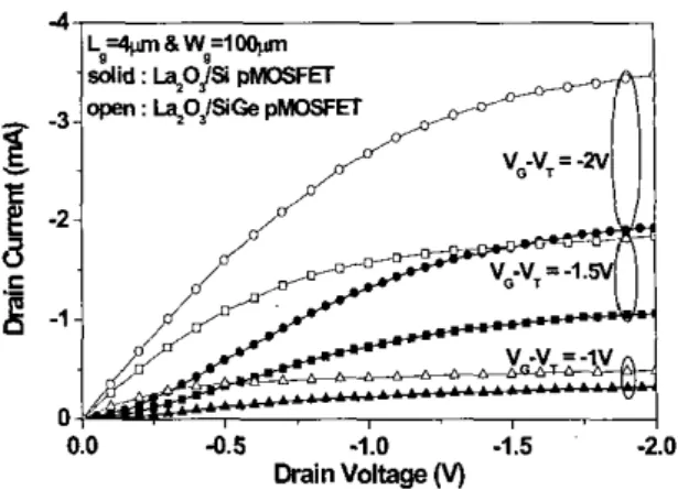
Fig. 4. The ID-V, characteristics of La20j/Si and La20a/Sio.,Geo.7 p-MOSFETs.
Fig. 4 shows the ID-VD characteristics of 4 pm La203/Si and La20j/Sio.3Geo.7 p-MOSFETs plotted at the same Vc-V,. Although a relatively large junction leakage of 1 x 10~' A/cm2 is measured. Besides the good device I-V characteristics, the Sio3Geo.7 has -2 times higher current driving capability than Si device at the same V, of -2V. Because the La20, was formed on Si and Sio.3Geo.7 on the same lot with identical inversion capacitance in Fig. 2, the higher hole current is not due to the different gate dielectric. The significantly higher hole current is especially important for high-speed circuit application, which is the fundamental motivation for continuously scaling down.
Because the improved hole current may come from both higher mobility and threshold voltage (V,) difference, we have further measured the transfer lD-Vc characteristics. Fig. 5 show the 1 0 - v ~ and hole effective mobility for both La201/Si and La10,/Sio.,Geo.7 p-MOSFETs respectively, where the VT difference is also included for the mobility extraction shown in Fig. 6.
I O '
Vos = - 0 3
4 si
extraction shown in Fig. 6. 1
o-2-
Vos = - 0 3 t Sil o 4
t S i G ea
910'-5
E
.-
1 0 ' 1 0.0 -0.5 -1.0 -1.5 Gate Voltage (v) .OFig. 5. The Io-VG characteristics of La20,/Si and La20,/Sio,,Geo.7 p-MOSFETs. The same loFF suggests no leakage degradation but with significantly higher ION.
t Universal hole si mobility 150
-
NH, annealed La,O,lSiGe -0- NH, annealed La20,1Sig
120 VI2
90-
E
I 60 I 30 0 0.0 0.2 0.4 0.6 0.8 1.0 E, (MV/cm)Fig. 6. The hole mobility of La20s/Si and La203/Sio3Geo, p-MOSFETs.
In additional to the higher saturation hole current than La203iSi devices, the Laz03/Siu.3Geo.7 p-MOSFETs have the same off-state current (IoFF) and lower VT. The lower VT in La?03/Sio.,Geo.7 device is due to smaller energy handgap in Siu.3Geu.7. Besides the small V, difference of 0.2 V, the large hole current improvement is primary coming from the higher mobility using Siu.,GeU.,. A peak hole mobility of 31 cm2/V-s is obtained in nitrided La203/Si p-MOSFET that is comparable with nitrided HfD2/Si [2]. In sharp contrast, the La203/Siu.,Geo.7 device shown in Fig.
6
has a higher hole mobility of 55 cm2/V-s that is 1.8 times higher than the La203/Si control devices without using SiGe. In additional to the comparable gate oxide integrity and loFF, the higher mobility and IoN indicate the superior device performance can be realized in nitrided high-k
Laz03
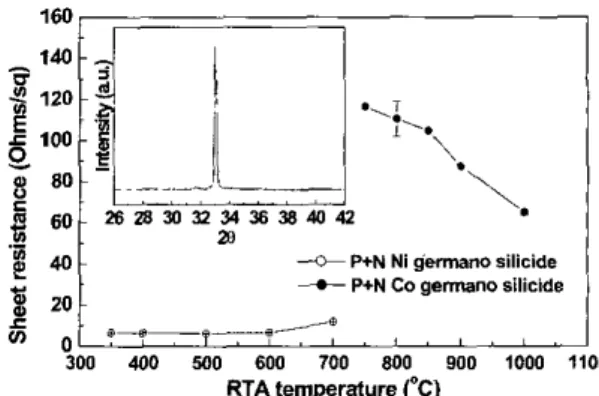
p-MOSFETs using solid-phase epitaxy formed SiGe. B. Ni germano-silicide:Figs. 7 and
8
show the sheet resistance of Ni and CO germano-silicide on @P and P% Sio.3Geo.7/Si junctions, respectively. The Ni germano-silicide exhibits superior sheet resistance than CO germano-silicide, and low sheet resistance of 6WO and 4RW are achieved on respective P'N and NIP junctions. From the XRD pattern inserted in Fig. 7, the formed phase is mono-germano-silicide that is the reason to achieve such low sheet resistance. The obtained low sheet resistance from 400 to 600 "C suggests Ni germano-silicide have good thermal stability and large process margin over this temperature range. We have used cross-sectional TEM to study the structure property of formed germano-silicide. Figs. 9 andIO show the Ni and
CO germano-silicide formed at 500 and 900 "C onN'P
Sio.,Geo,71Si junction, respectively. A relatively uniform thickness and smooth surface of Ni germano-silicide is observed, which explains the measured good s h e d resistance shown previously in Fig.
8.
In contrast, much rougher thickness and strong agglomeration are observed inCO
germano-silicide that gives the higher sheet resistance.We have further studied the junction characteristics of Ni germano-silicide. Figs. 1 1 and 12 show the junction
I
1: 117
20 U P+N Ni g e m n o silicide --e P+N CO germano Silicide300 400 M O 600 700 800 900 1000 1100 RTA temperature ("C)
Fig. 7. Sheet resistance comparison of CO and Ni germano-silicide on PIN Si,,Geo.,/Si.
g 1 0 0
""
c
-0- N+P Ni gemanasilidde-.-
N+P CO gemno-silicideI
.c 20 In Y 300 400 MO 600 700 800 900 1000 1100 RTA temperature (%)Fig. 8. Sheet resistance comparison of CO and Ni germano-silicide on N'P.
Fig.
9.
Cross-sectionalTEM of
CO germano-silicide on NIP Sio.,Geo.,/Si.Fig. 10. Cross-sectional TEM of Ni germano-silicide on N+P Si0.3Ge0.7iSi
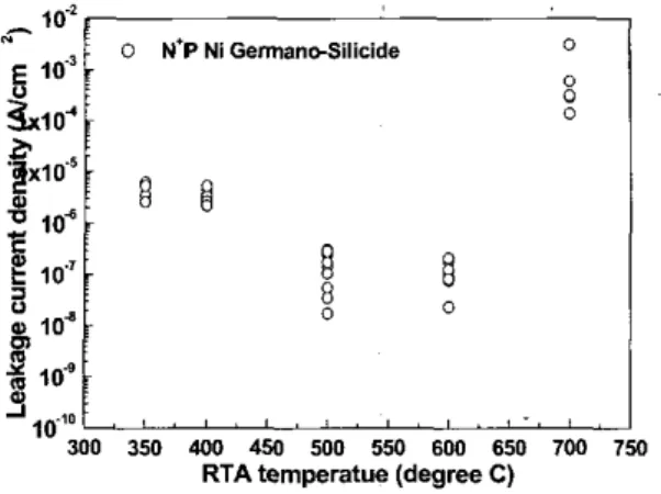
leakage current of Ni germano-silicide on P+N and
NIP
Sio.3Geu.71Si junctions, respectively. The possible reason may he due to the required higher silicidation temperature used for Co germano-silicide. The leakage current of P+N Ni germano-silicide junction decreases as silicidation temperature increasing from 300 to 500
“C,
and a minimum leakage current of < 3 ~ 1 0 - ~ Mcm2 is obtained at 500 OC formation temperature.-
10-2E
io-’
E
N%lo+
lo-^
:
IO“5
10.’:
I O *%
IO“ C m3
0 N’P Ni GennanOSilicide 0:
8
8
R
8
!
0Fig. 11. Junction leakage current of Ni germano-silicide on NIP
Sio ,Geo.,/Si.
-
10’-
p o 4 21x10sE
1 0 ‘ - 1 0 7 .:
104-I
a 1 0 s - 1 0 ‘ 09
g
._
U 1 ~ 0 P*N Ni Germano-Silicide - -8
0B
8
0 ’’
’ ”’
’’
’’
’ 3 ’ ”’
’Fig. 12. Junction leakage current of Ni germano-silicide on PIN Sio.3Geo~llSi.
Slightly raise
of
leakage currentwas
then found with the increasing silicidation temperature. The leakage current of NIP Ni germano-silicide junction shows the similar trend of temperature dependence to P’N junction, but a slightly higher minimum leakage current of <2x10~’ Ncm’is
obtained at 600OC. The drastically increaseof
leakage current at 700 “C may be due to the strong agglomeration at higher temperatures, whichis
also consistent with the rapid increasing sheet resistance at this temperature shown in Fig. 2.IV.
CONCLUSION
We have achieved -2 times higher ION and high hole mobility of 55 cm2N-s in nitrided La2031Sio.3Geo.l p-MOSFETs with almost identical gate oxide leakage current, capacitance density and loip. For SiGe MOSFET integration, Ni germano-silicide shows low sheet resistance of 4-6 010 is obtained on both P+N and NtP Sio3Geo.7/Si, and small junction leakage currents of <3xIO-’ and 2x10.’ Alcm2 are measured on respective junctions. The improved hole mobility in La203/Sio.,Geu.7 p-MOSFET and high quality Ni germano-silicide give another step to realize high-k gate dielectrics for VLSI integration.
ACKNOWLEDGEMENT
This work has been supported by GlobiTech Inc, USA.
REFERENCES
[ I ] Y. H. Kim, C. H. Lee, T. S. Jeon, W. P. Bai, C. H. Choi, S . J. Lee, L. Xinjian, R. Clarks, D. Roberts, and D. L. Kwong, “High quality CVD TaN gate electrode for sub-100nm MOS devices,” in IEDM Tech., Dig., 2001, pp. 667-670.
[2] K. Oishi, C. S. Kang, R. Choi, H.-J. Cho, S. Gopalan, R. Nieh, E. Dharmamjan, and J. C. Lee, “Reliability characteristic, including NBTI, of polysilicon gate HfO, MOSFET’s,” in IEDM Tech.. Dig., 2001, pp. 659-662.
[3] D. A. Buchanan, E.P. Gusev, E. Cartier, H. Okom-Schmidt, K.
Rim, M . A. Gribelyuk, A. Mocuta, A. Ajmera, M. Copel, S. Guha, N. Bojarcruk, A. Callegari, C. DEmic, P. Kozlowski, K.
Chan, R. J. Fleming, P.C. Jamison, 1. Brown, and R. Amdt, “80 nm poly-silicon gated n-FETs with ultra-thin AI,O, gate dielectric for ULSl applications,” in IEDM Tech., Dig. 2000,
pp. 223-226.
[4] A. Chin, C. C. Liao, C. H. Lu, W. J. Chen, and C. Tsai, “Device and reliability of high-k AI,O, gate dielectric with good mobility and low Dj,,” in Symp. on VLSI Tech.. 1999, pp.
135- 136.
[SI A. Chin, Y. H. Wu, S. B. Chen, C. C. Liao, W. J. Chen,
“High quality La2O3 and Al2O3 gate dielectrics with
equivalent oxide thickness 5-IOA,” in Symp. on VLSl
Tech.,2000, pp. 16-17,
[6] Y. T a u and T. K. Ning, Fundamentals of Modern VLSI
Devices, Cambridge, U.K.: Cambridge Univ. Press, 1998, p. 286.
S . Verdonckt-Vandebroek, E. F. Crabbe, B. S. Meyerson, D. L. Harame, P. J. Restle, J. M. C. Stork, and J. B. Johnson, “SiGe-channel heterojunction p-MOSFET’s,” IEEE Trans.
Electron Devices, vol. 41, no. I , pp. 90-101, 1994. [8] Y. H. Wu, W. J. Chen, A. Chin, and C. Tsai, “The effect of
native oxide on epitaxial SiGe from deposited amorphous Ge on Si,” Appl. Phys. Lett., vol. 74, no. 4, pp. 528-530, 1999. [9] Y. H. Wu and A. Chin, “High temperature formed SiGe
p-MOSFETs with goad device characteristics,” IEEE
Elecrron Device Lett., vol. 21, no. 7 , pp. 350-352, 2000. [IO] Y. H. Wu and A. Chin, “Gate oxide integrity of thermal oxide
grown on high temperature formed Sin3Geo.,,” IEEE
ElectronDeviceLett.,vol. 21,110. 3,pp. 113-115,2000. [ I I ] Y. H. Wu, A. Chin, and W. J. Chen, “Thickness dependent
gate oxide quality of thin thermal oxide grown on high temperature formed SiGe,” IEEE Electron Device Lett., vol. [7]
21, “0.6, pp, 2x9-291,2000.