國
立
交
通
大
學
電子工程學系 電子研究所
博 士 論 文
以噴射式大氣電漿在低溫下開發高品質二氧化矽應用在
低電壓操作之有機薄膜電晶體之研究
High-Quality Silicon Dioxide Developed by Atmospheric Pressure Plasma
Jet at Low Temperature for Low-Voltage OTFT Application
研 究 生:黃士軒
指導教授:張國明 教授
以噴射式大氣電漿在低溫下開發高品質二氧化矽應用在
低電壓操作之有機薄膜電晶體之研究
High-Quality Silicon Dioxide Developed by Atmospheric Pressure Plasma
Jet at Low Temperature for Low-Voltage OTFT Application
研 究 生:黃士軒 Student:Shih-Syuan Huang
指導教授:張國明 Advisor:Kow-Ming Chang
國 立 交 通 大 學
電子工程學系 電子研究所
博 士 論 文
A DissertationSubmitted to Department of Electronics Engineering and Institute of Electronics
College of Electrical and Computer Engineering National Chiao Tung University
in partial Fulfillment of the Requirements for the Degree of
Doctor of Philosophy in
Electronics Engineering June 2010
Hsinchu, Taiwan, Republic of China
i
以噴射式大氣電漿在低溫下開發高品質二氧化矽應用在
低電壓操作之有機薄膜電晶體之研究
學生: 黃士軒 指導教授: 張國明 博士 國立交通大學 電子工程學系電子研究所中文摘要
有機薄膜電晶體對許多研究者有很高的吸引力主要來自於它可以應用在可撓式顯示器以 及可撓式電子。可撓式顯示器可以用在電子紙,這可以減少樹木的砍伐,而可撓式電子方面 可以應用在人工皮膚、軟性感測器、RF-ID,雖然有機薄膜電晶體已經發展很長一段時間,但 是在有機薄膜電晶體的發展上仍然存在一些問題,主要包含低的電子遷移率、不穩定性、低 溫且低成本的製程、高操作電壓。在本論文中,由於塑膠基板不能承受高溫製程,低溫製程 的開發變得越來越重要,就我們所知要得到高品質絕緣層通常需要高溫處理,因此開發低溫 高品質的絕緣層將是非常困難的,製作絕緣層方法包含 PECVD、PVD 和溶液製程,PECVD 和 PVD 雖然廣泛被研究,但是都需要真空設備這將不利於大面積製作以及低成本的應用。溶液製程 雖然符合低成本需求,但是容易在薄膜中形成孔洞而且為了去除薄膜裡的溶劑需要長時間的 烘烤。 目前大多數的 OTFTs 都操作在高電壓約 -20 V~-40 V,這將會造成較高的功率損耗且不利 於應用在攜帶式電子產品。所以如何降低操作電壓是非常之重要的,目前通常利用高介電係 數材料以及較薄的絕緣層來當作閘極介電層,這可以增加單位面積的電容值去減少操作電ii 壓。 剛開始為了開發低溫且低成本製程,我們致力於利用大氣電漿技術去開發高品質二氧化矽 薄膜當做有機薄膜電晶體絕緣層。因為大氣電漿可以操作在低溫下且適合大面積低成本製程 的應用。在第二章我們分析溫度、流量、噴嘴距離、主要氣體對薄膜品質的影響。如我們期 待的,我們利用大氣電漿在基板溫度約為 150 O C 下成功開發出高品質的二氧化矽薄膜,漏電 流密度約為 2.53E-8 A/cm2 在 0.5 MV/cm,目前大多數研究所發表的絕緣層漏電流密度約為 1E-8~5E-6 A/cm2 at 0.5 MV/cm 且大多數不符合低溫低成本的製程,在第三章,為了減小操作 電壓我們絕緣層厚度控制在約 10 nm 來增加絕緣層單位面積的電容值,我們成功的將所開發 出來的高品質二氧化矽整合到低電壓操作的元件上,有機薄膜電晶體操作電壓小於 -2 V、截 止電壓約為 -0.8 V、電子遷移率約為 0.66 cm2 /V-s、次臨界電壓約為 700 mV/decade,大多 數研究者所發表出來的操作電壓通常大於 -20 V,我們在絕緣層品與元件特性有顯著的改 善。 在我們成功沉積高品質絕緣層後,對二氧化矽做表面處理將有助於改善主動層的分子排列, 這有助於電子遷移率的提升,但我們發現在做完表面處理後漏電流卻增加了,而這現象並沒 有被討論過,且我們認識為這將會限制未來短通道有機薄膜電晶體的發展,為了瞭解這現象 我們利用 top-contact 結構去討論表面處理對漏電流的影響在第四章。
iii
High-Quality Silicon Dioxide Developed by Atmospheric
Pressure Plasma Jet at Low Temperature for Low-Voltage
OTFT
Student: Shih-Syuan Huang Advisors: Kow-Ming Chang
Department of Electronics Engineering
& Institute of Electronics
National Chiao-Tung University
Hsinchu, Taiwan R.O.C.
Abstract
Organic thin film transistors (OTFTs) have lots of attraction for many researches because of their interesting and innovative applications on flexible display and flexible electronics. Flexible display could be used as an e-book which could reduce the use of woods. On the other hand, flexible electronics would be applied for artificial skin, flexible sensors, and RF-ID. Although OTFTs have been studied for a long time, there are still some issues influencing the development of OTFTs. These issues of OTFTs include low mobility, instability, low cost and temperature processes, and high operation voltage.
In this dissertation, we aim to develop low cost ant temperature processes of gate insulator and low-voltage OTFTs. Because the plastic substrate could not sustain high temperature processes, the development of low-temperature processed OTFTs is more and more important. As we known, to
iv
gain good film quality with a low leakage current, a high-temperature insulator activation is required. Therefore, it is very difficult to develop low temperature processes for high-quality gate insulator. Fabricating approaches of gate insulator include PECVD, PVD, and solution processes. PECVD and PVD are widely used to deposit insulator but they need a vacuum system and higher cost which are not suitable for large area application of flexible display. Although solution processes could decrease the cost, this method easily forms the pin-hole and needs a long-time baking for solvent-free.
In most researches, OTFTs operated at high voltage about -20 V ~ -60 V which would lead to high power consumption. Because the high power consumption is not suitable for portable electronics, how to reduce the operation voltage of OTFTs would be urgent for flexible display and flexible electronics. Therefore, many researches utilized high-k material or thin insulator as gate dielectric, increasing capacitance of per unit area dielectric, to reduce the operation voltage.
In the beginning, we aim at the development of low cost and temperature processes. We are devoted to use atmospheric pressure plasma jet (APPJ) for depositing high quality silicon dioxide (SiO2) as the gate insulator of OTFTs. Because APPJ could be operated at low temperature and
atmospheric pressure, it is suitable for large area and low cost application. In chapter 2, we analyzed the influence of substrate temperature, flow rate, gap distance, and main gas on the quality of SiO2.
As we expected, a low leakage current density of 2.53 E-8 A/cm2 at 0.5 MV /cm for SiO2 deposited
by APPJ at low temperature about 150 OC was demonstrated here. The leakage current density of most researches are between 1E-8~5E-6 A/cm2 at 0.5 MV /cm and most of them are not suitable for low cost and temperature processes.
In order to reduce operation voltage of OTFTs, the thickness of SiO2 was controlled about 10 nm
to increase the capacitance of per unit area dielectric. Low-voltage OTFTs were successfully integrated with APPJ-SiO2 which was described in chapter 3. These OTFTs showed a lower
v
and a good subthreshold swing about 700 mV/decade. We got obviously improvement on the performance of gate insulator and OTFTs by using APPJ.
After we successfully deposited high quality silicon oxide, surface treatment on the silicon oxide could be used to improve ordering of active layer which would increase mobility of OTFTs. However, we found that the leakage current would increase with a surface treatment. We consider this phenomenon would limit the development of short channel OTFTs. In order to understand the phenomenon, we utilized top-contact structure to discuss the influence of the surface treatment on leakage current in chapter 4.
vi
致謝
首先非常感謝我的指導老師張國明教授,感謝張教授在研究上的細心的指導與大力的支持, 使得研究過程中可以克服萬難順利完成論文。 再來感謝實驗室學長趙高毅、林建宏、林稔杰、林志祥、陳柏寧、鄧一中、大俊銘、小俊 銘、淳哥等,謝謝學長們不論在生活或研究上都給予許多意見及幫忙,在感謝學弟蘇俊榮、 阿茂、菘宏、明頤、堃豪、彥凱、成家、阿葉、阿信、阿賢的幫忙與陪伴,讓研究生活更豐 富。 另外感謝交通大學奈米中心以及國家奈米實驗室在實驗器材上的大力支持,感謝兩個機構 中許許多多的研究人員以及技術人員這些年提供的幫助。還有感謝我敬愛的父母親、姐姐的 陪伴與支持,讓我在念博士班期間有很大的精神支柱。vii
Contents
Chinese Abstract ………...………... i
English Abstract ………...…iii
Acknowledgment……….... vi
Contents………. vii
Table Caption………...……….. ix
Figure Captions………..…. x
Chapter 1 Introduction………...1
1.1 History & Application of OTFTs………1
1.2 Operation Theory of OTFTs………...…2
1.3 Major Issues for OTFTs Development………...4
1.4 Overview of Dissertation………....6
1.5 References………..…..14
Chapter 2 Development of Low-Temperature and High-Quality Silicon Oxide Processed by Atmospheric Pressure Plasma Jet……...20
2.1 Effect of Growth Rate Influenced by Substrate Temperature on Different Substrate Materials………..….20
2.1.1 Introduction………...20
2.1.2 Experiment………....21
2.1.3 Results and Discussion……….……….…23
References………...33
2-2 The Effect Flow Rate on The Surface Morphology and Film Quality………34
References………..41
viii
2.4 The Effect of Main Gas on The Deposition Rate and Electrical
Characteristics………..………47
2.4.1 Introduction……….…..47
2.4.2 Experiment………....47
2.4.3 Results and Discussion………...…………...48
References………..………57
Chapter 3 Characterization and Discussion of Low-Voltage OTFT Devices with a Atmospheric-Deposited SiO2 Introduction………...……….58
3.2 Experiment………..…….58
3.3 Results and Discussion……….59
References………..66
Chapter 4 The Investigation of Electrical Characteristic Dependent of Surface Hydrophobic Treatment………...………….…67
4.1 Introduction………..67
4.2 Experiment………..……….…68
4.3 Results and Discussion………..……….……..69
4.4 Conclusions………..…………....71
References………..………....78
Chapter 5 Conclusion and Future Work………...79
5.1 Conclusion……….…………...79
5.2 Future Work……….………81
ix
Table Caption
Table 2-2-1 The details of experimental parameters of silicon oxide deposited with different flow rates by APPJ.
Table 2-2-2 The concentration of carbon in silicon oxide, deposited with different flow rates, was analyzed by X-ray Photoelectron Spectroscopy.
Table 2-3-1 Experimental parameters of APPJ-SiO2 deposited with different gap distances.
Table 2-3-2 Thickness and deposition rate of APPJ-SiO2 deposited with different gap distances.
Table 2-3-3 The leakage current density and surface roughness of silicon oxide deposited with different gap distances
Table 2-4-1 Experimental parameters of APPJ-SiO2 deposited with different main gases.
Table 2-4-2 Leakage current density (A/cm2 ) of APPJ-SiO2 at 0.5 MV/cm with different main
gases.
Table 2-4-3 Deposition rate and thickness of SiO2 deposited with different main gases of
atmospheric pressure plasma jet.
Table 2-4-4 Composition of silicon oxide fabricated with different main gases of atmospheric pressure plasma jet.
Table 3-1 Comparison of this work with other researches about the characteristics of OTFTs fabricated at low temperature processes or operated at low voltage.
x
Figure Caption
Figure 1-1 Flexible displays announced by LG.
Figure 1-2 Photo of OTFT-driven OLED display wrapped around a cylinder with 4 mm radius. (Sony Corp.)
Figure 1-3 2T-1C OTFT driven OLED pixel design
Figure 1-4 Electronic artificial skin integrated pressure and temperature sensors. Made by Prof. Takao Someya, University of Tokyo in Ref. [22].
Figure 1-5 Top contact structure (a) and Bottom structure (b) of OTFTs
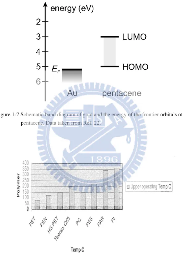
Figure 1-6 Output (a) and transfer (b) characteristics of a typical OTFT. The inset shows the molecular structure of pentacene, which serves as semiconductor in the device. Figure 1-7 Schematic band diagram of gold and the energy of the frontier orbitals of pentacene.
Data taken from Ref. 22.
Figure 1-8 Upper processing temperature of flexible substrate.
Figure 1-9 Schematic of the atmospheric-pressure plasma jet for the deposition of silicon oxide. Figure 2-1-1 MIM structure for testing gate insulator’ quality.
Figure 2-1-2 Scheme of the top contact structure of organic thin transistor
Figure 2-1-3 (a) capacitance vs. voltage (C-V) of SiO2 deposited by APPJ and E-gun. (b) Leakage
current density vs. electric field (J-E) of SiO2 respectively deposited by APPJ and
E-gun.
Figure 2-1-4 J-E of SiO2 respectively deposited by APPJ and E-gun in MIM structure. Leakage
current density of SiO2 (APPJ), deposited at 150 oC, was about 1E-7 A/cm2 at 0.5
MV/cm.
Figure 2-1-5 Thickness (a) and leakage current density (b) of silicon oxide deposited on the Al/amorphous silicon at room temperature.
xi
Figure 2-1-6 Thickness and leakage current density of silicon oxide deposited on the Al/amorphous silicon at room temperature.
Figure 2-1-7 Scheme of the output characteristics of pentacene-based organic thin film transistor with a lower operation voltage about -3 V.
Figure 2-1-8 Scheme of transfer characteristics of penetacene-based organic thin film transistor with mobility about 0.066 cm2/V-S.
Figure 2-1-9 (a) AFM image of aluminum gate electrode with roughness about 8.7 nm.
(b) AFM image silicon oxide deposited at 150 ℃ on the aluminum with the roughness around 10.8 nm
Figure 2-1-10 Scheme of the RMS of silicon oxide deposited at different temperatures separately on Al and Ni.
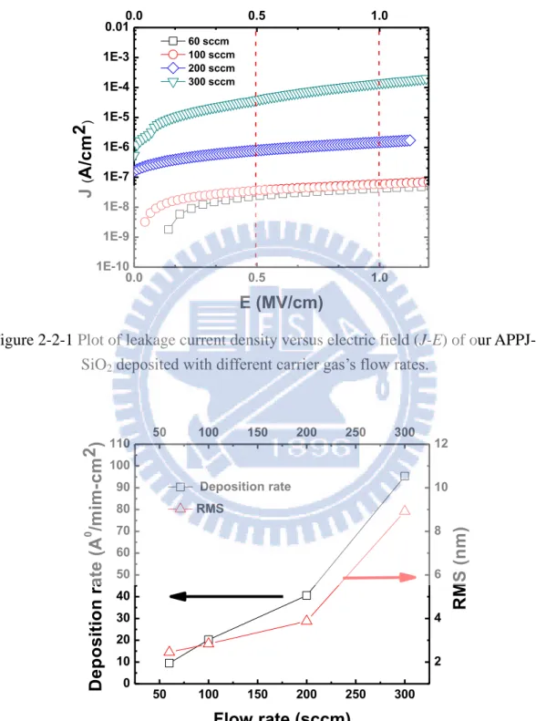
Figure 2-2-1 Plot of leakage current density versus electric field (J-E) of our APPJ- SiO2 deposited
with different carrier gas’s flow rates.
Figure 2-2-2 Deposition rate and RMS of silicon oxide deposited with different flow rates of atmospheric pressure plasma jet.
Figure 2-2-3 AFM images of silicon oxide fabricated with different Ar flow rates of APPJ. (a) 60 sccm (b) 100 sccm (c) 200 sccm (d) 300 sccm
Figure 2-2-4 SEM images of silicon oxide fabricated with different Ar flow rates of atmospheric pressure plasma jet. (a) 60 sccm (b) 100 sccm (c) 200 sccm (d) 300 sccm Figure 2-2-5 X-ray Photoelectron Spectroscopy spectra of SiO2 (APPJ) deposited with different Ar
flow rates.
Figure 2-3-1 Schematic diagram of gap distance of APPJ. Gap distance means the distance from nozzle to the surface of sample.
Figure 2-3-2 Deposition rate and RMS of APPJ-SiO2 deposited with different gap distances.
xii
distances.
Figure 2-4-1 Main gas was introduced into the high electric field region between electrodes of APPJ for generating plasma.
Figure 2-4-2 Electric field versus leakage current density of silicon oxide with different main gases of atmospheric pressure plasma jet.
Figure 2-4-3 Deposition rate and surface roughness of silicon oxide deposited by different main gases.
Figure 2-4-4 AFM images of silicon oxide fabricated with different main gases of atmospheric pressure plasma jet. (a) CDA (b) N2 (c) O2
Figure 2-4-5 SEM images of silicon oxide fabricated with different main gases of atmospheric pressure plasma jet. (a) CDA (b) N2 (c) O2
Figure 2-4-6 X-ray Photoelectron Spectroscopy survey spectra from silicon oxide fabricated with different main gases of atmospheric pressure plasma jet.
Figure 2-4-7 The leakage currents of silicon oxide deposited with different main gases are plotted as functions of electric field on ln J – E1/2 scales. Using CDA as main gas could get lower leakage current.
Figure 3-1 Leakage current density of silicon oxide showed the breakdown voltage was about 8 MV/cm.
Figure 3-2 Fabrication processes of organic thin film transistors. Figure 3-3 Output characteristics (ID-VDS) of OTFTs.
Figure 3-4 Transfer characteristics (ID-VG) and |ID|1/2-VG of OTFTs.
Figure 4-1 A cross-section plot of a top contact OTFT with surface treatment of gate insulator. Figure 4-2 Transfer characteristics of OTFTs fabricated with various surface treatments.
Figure 4-3 UV-vis absorption spectra of P3HT films that are deposited on SiO2 dielectric layers following various surface treatments , normalized to the maxima of the spectra.
xiii
Figure 4-4 (a) IDS-VDS of OTFTs with and without surface treatment without patterning the active
region. (b) A diagram of holes moving direction at source and drain are zero voltage. Figure 4-5 (a) IDS-VGS of OTFTs with and without surface treatment without patterning the active
region. (c) A diagram of holes moving direction when an OTFT was at static state. Figure 4-6 (a) IG versus VG of OTFTs with and without surface treatment when source is floating.
(b) The measurement condition and hole moving direction of the OTFT.
Figure 4-7 IDS-VDS of OTFTs with and without patterning active region after surface treatment.
1
Chapter 1 Introduction
1.1 History & Application of OTFTs
Semiconductors have been widely used in various electronic devices. In addition, the invention of semiconductor transistor took replacement of traditional vacuum tube based electronics. Silicon is the dominate material in the use of high performance electronic chip from the end of 20th century and lead to the omnipresence of semiconductor microelectronics in our daily life. Organic semiconductor materials have been widely studied for the expectation of new applications, such as flexible light sources [1-5], flexible display [6-11], flexible electronics [12-14], and plastic solar cells [15-17]. In recent years, Flat panel displays (FPD) are growing quickly because flat panel displays are lighter, much thinner, and less power than traditional cathode ray tube (CRT). The development of flat panel display has made great progress in resolution, brightness, contrast ratio, viewing angle, response time, weight and so on. FPD are widely used in mobile phone, notebook, camera, and television and become more and more important for our life. Flexible displays are considered as the revolutionary product because it could be applied for e-paper, e-book, and large area screen which would decrease the use of woods, keep environment, and make our life colorful. Therefore, many national companies focus their investigation and development on the flexible display such as PVI, AUO, Fujitsu, Samsung Electronics, Sony, LG, and so forth. Figure 1-1 showed the pictures of the flexible display announced by LG. Recently, Sony Corporation announced that they developed a super-flexible 80 μm-thick, 4.1-in, 121 ppi, and OTFT-driven full color OLED display which can be wrapped around a thin cylinde at SID (Society for Information Display) 2010 International Symposium on May 27. Flexible display announced by Sony
2
Corporation was shown in Figure 1-2.
Organic thin film transistors (OTFTs) play an important role of flexible display and have been widely studied by many researchers. Pixel of active matrix organic light-emitting displays (AM-OLED) was shown in Figure 1-3. OTFTs could be used to charge the capacitor and drive the OLED in the pixel of AM-OLED and as a key component. In addition, OTFTs were also applied for flexible electronics, including ratio frequency identification smart card (RFID) and sensors such as pressure sensor, gas sensor, bio-sensor, and electronic artificial skin [18-23], shown in the Figure 1-4. In the following sections, we would introduce the operation theory, fabrication methods, and major issues of OTFTs. Also, atmospheric pressure plasma jet (APPJ) with many advantages, applied for OTFTs fabrication would be introduced in the following sections, simultaneously.
1-1 Operation Theory of OTFTs
The structures of OTFTs mainly included two types of top contact (TC) and bottom contact (BC) [24-27], respectively, shown in Figure 1-5 (a) and (b). The structures of OTFTs have several variants. In general, an OTFT is composed of four parts – a metal electrode, an insulator, a thin channel layer, and the sourc/drain metal contacts. Each of these structures has its advantages and drawbacks. In the BC structure, source-drain electrodes deposited on insulator could be patterned by lithographic technology to get higher device density. However, source-drain electrodes could not be defined by lithographic technology in TC structure. This is because the organic semiconductor materials are much easier influenced by oxygen, water, organic solvent [28-29], and so on. Therefore, most TC structures need to pattern the source-drain electrodes by shadow mask but then decrease the densities of OTFT devices. In addition, TC
3
structures with lower contact resistance than BC structure could increase the mobility of OTFTs due to its channel material with better molecule ordering and larger grain size.
Transfer characteristics (ID-VG) and output characteristics (ID-VD) of OTFTs are
shown in the Figure 1-6 (a) and (b). These curves were measured on the pentacene-based OTFTs made with gold source and drain electrodes. The chemical structure of pentacene was also inserted in Figure 1-6 (a). Figure 1-7 shows the energy scheme which indicates the respective positions of the Fermi level of gold and the frontier orbitals (highest occupied molecular orbital, HOMO, and lowest unoccupied molecular orbital, LUMO) of pentacene. The LUMO level of pentacene is quite far away from the Fermi level of gold, so there is a substantial energy barrier for electrons. Therefore, electron injection is very difficult when a positive voltage is applied to the gate and source is connected with ground. In contrast, holes can be injected to the semiconductor from the source by applying a reverse gate voltage, since the Fermi level of gold is close to the HOMO level of pentacene. With increasing reverse gate voltage, the hole conductive channel forms at the interface between insulator and semiconductor. The hole charge could be driven from source to drain by applying negative voltage to the drain. It is a reason that pentacene is call as a p-type semiconductor. However, this concept is obviously different to the common p-type or n-type materials doped by implanting. In another words, when the source and drain electrodes can inject electrons into its LUMO level, an organic semiconductor will be a n-type material.
Generally, the gate voltage of OTFTs could induce the equal charges at both sides of gate insulator. These injected charge carriers increase as applying a reverse gate voltage and then generate a conductive channel with high conductance.. At low drain voltage, the current almost follows Ohm’s law especially using high work function
4
source-drain metal material. Therefore, OTFTs are mainly controlled by gate and drain voltages. As the drain current approaches to the gate voltage, the channel gradually becomes pinch off. Then, the channel current becomes independent to drain bias which is called saturation region. The mobility of OTFTs was extracted in saturation region from the following equation:
( )2 2 G T DS V V L WCi I [1]
Where W and L are the channel width and length, Ci is the insulator capacitance
per unit area, VG and VD are the gate and drain voltage, and VT is the threshold
voltage that takes into account various potential drops through the gate-insulator- semiconductor structure. In the saturation region, μ can be calculated from the slope of the plot of |ID|1/2 versus VG.
1-2 Major Issues for OTFT Development
Organic thin film transistor are expected to be applied for flexible display. In recent years, although the performance of OTFTs have great improvement, there are still some issues influencing the development of OTFTs. These issues of OTFTs mainly include low mobility, stability, and high operation voltage.
The mobility of organic thin film transistors is only about 0.001~10 cm2/V-s, much lower than silicon-base MOSFET and polysilicon TFT. The mobility of OTFTs is dominated by organic material and ordering of organic material [30-32]. On the other hand, stability of organic semiconductor material is a serious problem. Electrical characteristics of OTFTs would be degraded by oxygen, moisture, and organic solvent
5
and so on [28, 29]. Some researchers believed that oxygen would diffuse into active layer and formed impurities in the organic semiconductor layer but these studies resulting from environment influence are not very clear. These environment factors may lead to the degradations of on current, threshold voltage shift, and subthreshold swing. It is well known that lithography processes such as organic solvent, photoresistor, water, exposure, and baking may degrade the performance of OTFTs. Therefore, there are many researchers focus on fabrication of capping layer [33, 34] and some of studies endeavor to overcome the issue of active layer tied to lithography processes[35, 37], which are important for the improvement on device performance and circuit density.
However, another pending problem of OTFTs is high operation voltage [38-41]. The high operation voltage would result in high active power consumption, not suitable for the low-power protable electronics. Active power consumption is on current multiplied by operation voltage. However, we could not decrease the on current because higher on current could increase operation speed to overcome RC time delay. Therefore, decreasing operation voltage is urgent for OTFTs. In order to keep the magnitude of on current and decrease operation voltage, increasing the capacitance per unit area is the one of the ways to obtain the goal. Capacitance is positive proportional to dielectric constant and negative proportional to thickness of insulator. Therefore, many studies used high-k material or thinner insulator as the gate insulator to decrease the operational voltage [11-16]. Gate insulator materials mainly consist of polymer, metal oxide, and nanocomposite. Polymer is suitable for low cost processes such as spin, inject, and print. However, the drawbacks of polymer include lower dielectric constant, longer baking time, and more holes pin-holes. Metal oxide materials usually have high dielectric constant such as HfO2, Ta2O5, TiO2, Al2O3, AlN,
6
high cost and low throughput processes for flexible electronics. Metal oxide material usually need a high temperature anneal to improve quality which is not suitable for plastic substrate. Plastic substrate usually could not sustain over 200 oC and the upper processing temperature of different kinds flexible substrate are shown in Figure 1-8.
1-4 Overview of Dissertation
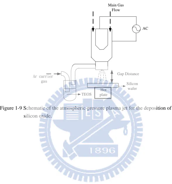
Organic thin film transistors attracted many researchers and company to investigate and develop due to their future applications. Some main issues including low mobility, stability, and high operation voltage had been described above. In our work, we focus on developing and investigating low temperature and low cost processes to fabricate high quality silicon oxide as a gate insulator for OTFTs. Silicon dioxide is a kind of very cheap and rich resource in the world and used as main gate insulator for MOSFET. Band gap of silicon dioxide is about 9 eV which is good to be used as a gate insulator. In addition, good stability and reliability of silicon oxide were also proposed in many researches. The highest process temperature of OTFTs usually happened in gate insulator. So decreasing the processes temperature of gate insulator is very important for OTFTs due to the plastic substrate could not sustain high temperature. For the purpose of low cost and high throughput processes, atmospheric pressure plasma jet (APPJ) was utilized in this thesis. We controlled our processes temperature from room temperature to 200 oC. There are lot of advantages of APPJ such as low temperature, low cost, and high throughput.
Figure 1-9 shows the basic structure of atmospheric pressure plasma jet. Because APPJ could be operated in atmospheric pressure it is suitable for large area application which is very important for cost down.. Good quality of silicon oxide deposited by APPJ had been developed by us and leakage current density was
7
suppressed below 1~2E-8 A/cm2 at 0.5 MV/cm in MIM structure. We controlled temperature, flow rate, gap distance, and main gas to improve the performance of silicon oxide which were all described in chapter 2. In addition, silicon oxide deposited with APPJ was successfully applied for the gate insulator of OTFTs. The thickness of our demonstrated silicon oxide is only 9 nm so the operation voltage of OTFTs was about -2 V. Threshold voltage is about 0.8 V, mobility is about 0.66 cm2/V-s, and subthreshold swing is about 0.6 V/decade in our proposed OTFTs. The detail fabrication and discussion of OTFTs were described in chapter 3. We found that higher molecular ordering of organic semiconductor would influence the leakage current of OTFTs. Many studies used surface treatment to improve the molecular ordering of channel layer and increase the mobility of OTFTs. However, leakage current of OTFTs was also increased after improving molecular ordering and this drawback was ignored. We used to contact structure of OTFTs to investigate and discuss this problem in this chapter 4.
8
Figure 1-1 Flexible displays announced by LG.
Figure 1-2 Photo of OTFT-driven OLED display wrapped around a cylinder with 4 mm radius. (Sony Corp.)
9
Figure 1-3 2T-1C OTFT driven OLED pixel design
Figure 1-4 Electronic artificial skin integrated pressure and temperature sensors. Made by Prof. Takao Someya, University of Tokyo in Ref. [22].
10
Source
Drain
Active layer
Substrate
Gate
Gate insulator
(a)Substrate
Source
Active layer
Drain
Gate
Gate insulator
(b)
11
(a)
(b)
Figure 1-6 Output (a) and transfer (b) characteristics of a typical OTFT. The
inset shows the molecular structure of pentacene, which serves as semiconductor in the device.
12
Figure 1-7 Schematic band diagram of gold and the energy of the frontier orbitals of pentacene. Data taken from Ref. 22.
13 AC Main Gas Flow Ar carrier gas TEOS Silicon wafer Hot plate Gap Distance
Figure 1-9 Schematic of the atmospheric-pressure plasma jet for the deposition of silicon oxide.
14
Reference
[1] C. K. Han, H. K. Kim, H. S. Pang, S. H. Pieh, and Y. H. Tak, “Dual-Plate OLED Display (DOD) Embedded With White OLED,” Journal of Display Technology, vol. 5, no. 12, pp. 541-545, Dec. 2009.
[2] S. W. Wen, M. T. Lee, and C. H. Chen, “Recent Development of Blue Fluorescent OLED Materials and Devices,” Journal of Display Technology, vol. 1, no. 1, pp. 90-99, Sept. 2009.
[3] Si Yujuan, Zhao Yi, Chen Xinfa, and Liu Shiyong, “A Simple and Effective ac Pixel Driving Circuit For Active Matrix OLED,” IEEE Trans. Electron Devices, vol. 50, no. 4, pp. 1137-1140, Apr. 2003.
[4] A. Sugimoto, H. Ochi, S. Fujimura, A. Yoshida, T. Miyadera, and M. Tsuchida, “Flexible OLED Displays Using Plastic Substrates,” IEEE Journal of Selected Topics in Quantumelectronics, vol. 10, no. 1, pp. 107-114, Jan. 2004.
[5] K.H. Kim, J.Y. Lee, T.J. Park, W.S. Jeon, G.P. Kennedy, J.H. Kwon, “Small molecule host system for solution-processed red phosphorescent OLEDs,” Synthetic Metals, vol. 160, issue 7-8, pp. 631-635, Apr. 2010.
[6] L. Hu, J. Li, J. Liu, G. Grüner, and T. Marks, “Flexible organic light-emitting diodes with transparent carbon nanotube electrodes: problems and solutions,” Nanotechnology, vol.21, Mar. 2010.
[7] C. D. Sheraw, L. Zhou, J. R. Huang, D. J. Gundlach, T. N. Jackson, M. G. Kane, I. G. Hill, M. S. Hammond, and J. West, “Organic thin-film transistor-driven
polymer-dispersed liquid crystal displays on flexible polymeric substrates,” Appl. Phys. Lett. vol. 80, no. 6, pp 1088-1090, Feb. 2002.
[8] H. Klauk, D. J. Gundlach, J. A. Nichols, and T. N. Jackson, “Pentacene organic thin-film transistors for circuit and display applications,” IEEE Trans. Electron
15
Devices, vol. 46, no.6, pp. 1258-1263, Jun. 1999.
[9] H. Suzuki, H. Fukagawa, and Y. Nakajima, “A 5.8-in. phosphorescent color AMOLED display fabricated by ink-jet printing on plastic substrate,” Journal of The Society for Information Display, vol. 17, no.12, pp. 1037-1042, Dec. 2009. [10] Y. Fujisaki, H. Sato, T. Yamamoto, “Flexible color LCD panel driven by
low-voltage-operation organic TFT,” Journal of The Society for Information Display, vol. 15, no.7, pp. 501-506, Dec. 2007.
[11] S. H. Han, Y. H. Kim, S. H. Lee, “Stable organic thin-film transistor in a pixel for plastic electronics,” Organic Electronics, vol. 9, no. 6, pp. 1040-1043,Dec. 2008. [12] Y. Y. Lin, A. Dodabalapur, R. Sarpeshkar, Z. Bao, W. Li, K. Baldwin, V. R. Raju,
and H. E. Katz, “Organic complementary ring oscillators”, Appl. Phys. Lett., vol. 80, no. 7, pp 2714-2716, Feb. 1999.
[13] P. F. Baude, D. A. Ender, M. A. Haase, T. W. Kelley, D. V. Muyres, and S. D. Theiss, “Pentacene-based radio-frequency identification circuitry,” Appl. Phys. Lett. vol. 82, no. 22, pp 3964-3966, Apr. 2003.
[14] M. G. Kane, J. Campi, M. S. Hammond, H. Klauk, and T. N. Jackson, “Analog and Digital Circuits Using Organic Thin-Film Transistors on Polyester
Substrates,” IEEE Electron Device Lett., vol. 21, no. 11, pp. 534-536, Nov. 2000. [15] W. W. Li, Y. Han, and Y. L. Chen, “Polythiophenes with Carbazole Side Chains:
Design, Synthesis and Their Application in Organic Solar Cells,”
Macromolecular Chemistry and Physics, vol. 211, no. 8, pp. 948-955, Apr. 2010. [16] S. Berson, S. Cecioni, and M. Billon, “Effect of carbonitrile and hexyloxy
substituents on alternated copolymer of polythiophene-Performances in photovoltaic cells,” Solar Energy Materials and Solar Cells, vol. 94, no. 5, pp. 699-708, May 2010.
16
Abatement in Semiconductor and Solar Cell Fabrication with Respect to Resource Depletion,” Chemical Engineering & Technology, vol. 33, no. 4, pp. 638-646, Apr. 2010.
[18] T. Someya, Y. Kato, and T. Sekitani, “Conformable, flexible, large-area networks of pressure and thermal sensors with organic transistor active matrixes,”
Proceedings of The National Academy of Sciences of The United States of America, vol. 102, no. 35, pp.12321-12325 Aug. 2005
[19] T. Someya, T. Sekitani, and S. A. Iba, “Alarge-area, flexible pressure sensor matrix with organic field-effect transistors for artificial skin applications,” Proceedings of The National Academy of Sciences of The United States of America, vol. 101, no. 27, pp.9966-9970, Jul. 2004.
[20] T. Sekitani, T. Yokota, U. Zschieschang, H. Klauk, S. Bauer, K. Takeuchi, M. Takamiya, T. Sakurai, and T. Someya, “Organic Nonvolatile Memory Transistors for Flexible Sensor Arrays,” Science, no. 326 (5959), pp.1516-1519, Dec. 2009. [21] M. E. Roberts, S. C. B. Mannsfeld, and N. Queralto, “Water-stable organic
transistors and their application in chemical and biological sensors,” Proceedings of The National Academy of Sciences of The United States of America, vol. 105, no. 34, pp.12134-12139, Aug. 2008.
[22] I. Manunza, and A. Bonfiglio, “Pressure sensing using a completely flexible organic transistor,” Biosensors & Bioelectronics, vol. 22, no.12, pp. 2775-2779, Jun. 2007.
[23] J. W. Jeong, Y. D. Lee, Y. M. Kim, “The response characteristics of a gas sensor based on poly-3-hexylithiophene thin-film transistors,” Sensors and Actuators B-Chemical, vol. 146, no. 1, pp. 40-45, Apr. 2010.
[24] S. H. Jin, K. D. Jung, H. Shin, B. G. Park, and J. D. Lee, “Grain size effects on contact resistance of top-contact pentacene TFTs,” Synthetic Metals vol. 156, pp.
17
196–201, 2006.
[25] K. D. Jung, Y. C. Kim, B. J. Kim, B. G. Park, H. Shin, and J. D. Lee, “An Analytic Current–Voltage Equation for Top-Contact Organic Thin Film Transistors Including the Effects of Variable Series Resistance,” Jpn. J. Appl. Phys., vol. 47, pp. 3174-3178, 2008.
[26] D. Gupta, and M. Katiyar, “An analysis of the difference in behavior of top and bottom contact organic thin film transistors using device simulation,” Organic Electronics, vol. 10, no. 5, pp. 775-784, Aug. 2009.
[27] K. D. Jung, Y. C. Kim, and H. Shin, “A study on the carrier injection mechanism of the bottom-contact pentacene transistor,” Appl. Phys. Lett. vol. 96, no. 10, Mar. 2010.
[28] M. W. Lee and C. K. Song, “Oxygen Plasma Effects on Performance of Pentacene Thin Film Transistor,” Jpn. J. Appl. Phys., vol. 42, pp. 4218-4221, 2003.
[29] E. J. Meijer, C. Tanase, P. W. M. Blom, E. van Veenendaal, B.-H. Huisman, D. M. de Leeuw, and T. M. Klapwij, “Switch-on voltage in disordered organic field-effect transistors,” Appl. Phys. Lett. vol. 80, pp. 3838, 2002
[30] S. Y. Kwak, C. G. Choi, and B. S. Bae, “Effect of Surface Energy on Pentacene Growth and Characteristics of Organic Thin-Film Transistors,” Electrochemical and Solid State Letters, vol. 12, no. 8, pp. G37-G39, 2009.
[31] S. Y. Kim, T. Ahn, and S. Pyo, ”Surface modified polymeric gate insulators for pentacene organic thin-film transistors,” Current Applied Physics, vol. 9, no. 5, pp. 913-918, Sep. 2009.
[32] P. Marmont, N. Battaglini, P. Lang, G. Horowitz, J. Hwang, A. Kahn, C. Amato, and P. Calas, “Improving charge injection in organic thin-film transistors with thiol-based self-assembled monolayers,” Organic Electronics, vol. 9, pp. 419-424,
18
2008.
[33] G. W. Hyung, J. Park, and J. H. Kim, “Storage stability improvement of pentacene thin-film transistor using polyimide passivation layer fabricated by vapor deposition polymerization,” Solid-State Electronics, vol. 54, no. 4, pp. 439-442, Apr. 2010.
[34] H. N. Lee, Y. G. Lee, I. H. Kob, E. C. Hwang, and S. K. Kang, “Organic passivation layers for pentacene organic thin-film transistors,” Current Applied Physics, vol. 8, no. 5, pp. 626-630, Aug. 2008.
[35] W. S. Wong, K. E. Paul, and R. A. Street, “Digital-lithographic processing for thin-film transistor array fabrication,” Journal of Non-Crystalline Solids,” vol. 338-340, no. 15, pp. 710-714, Jun. 2004.
[36] Z. B. Ding and B. Ganem, “of patterned organic thin film by low-energy electron beam lithography and surface-initiated ring-opening metathesis polymerization,” Canadian Journal of Chemistry-revue Canadienne De Chimie, vol. 84, no. 10, pp. 1254-1258, Oct. 2006.
[37] I. Kymissis, A. I. Akinwande, and V. Bulovic “A Lithographic Process for Integrated Organic Field-Effect Transistors,” Journal of Display Technology, vol. 1, no. 2, pp. 289-294, Dec. 2005.
[38] Y. X. Lu, W. H. Lee, H. S. Lee, “Low-voltage organic transistors with titanium oxide/polystyrene bilayer dielectrics,” Appl. Phys. Lett., vol. 94, no. 11, pp. 3838, 2009.
[39] L. A. Majewski, R. Schroeder, and M. Grell, “Low-Voltage, High-Performance Organic Field-Effect Transistors with an Ultra-Thin TiO2 Layer as Gate Insulator,” Adv. Funct. Mater. Vol. 15, no. 6, pp. 1017-1022, 2005.
[40] S. Ono, S. Seki, R. Hirahara, Y. Tominari, and J. Takeya, “High-mobility,
19
Appl. Phys. Lett., vol. 92, no. 10, pp. 103313, 2008.
[41] Y. Jang, D. H. Kim, Y. D. Park, J. H. Cho, M. Hwang, and K. Cho, “Low-voltage and high-field-effect mobility organic transistors with a polymer insulator,” Appl. Phys. Lett., vol. 88, no. 7, pp. 072101, 2006.
[42] C. Bartic, H. Jansen, and A. Campitelli, “Ta2O5 as gate dielectric material for low-voltage organic thin-film transistors,” ORGANIC ELECTRONICS, vol. 3, no. 2, pp. 65-72, 2002.
[43] F. M. Li, A. Nathan, and Y. L. Wu, “Organic thin-film transistor integration using silicon nitride gate dielectric,” Appl. Phys. Lett., vol. 90, no. 13, pp. 133514, 2007.
[44] Y. H. Kim, J. H. Kwon, and S. I. Shin, “Organization of Pentacene Molecules on Anisotropic Ultrathin HfO2/Al2O3 Templates for Organic Thin-Film Transistors Using an Ion-Beam Treatment,” Electrochemical and Solid State Letters, vol. 12, no. 8, pp. H305-H308, 2009.
[45] W. H. Lee, C.C. Wang, W. T. Chen, and J. C. Ho, “Characteristic of Organic Thin Film Transistor with a High-k Insulator of Nano-TiO2 and Polyimide Blend,” Jpn. J. Appl. Phys., vol. 47, pp. 8955-8960, 2008.
20
Chapter 2
Factors for SiO2 Deposition by Atmospheric Pressure
Plasma Jet
In this chapter, we aim at depositing high quality silicon oxide at low temperature by atmospheric pressure plasma jet (APPJ). First, we discussed the temperature influence on deposition of silicon oxide and defined the deposition temperature of silicon oxide. Second, because carrier gas’s flow rate may influence the deposition rate and the quality of silicon oxide, we discuss the flow rate of carrier gas in section 2-2. We also found that the gap distance between nozzle and sample surface and main gas would influence the deposition rate and quality of silicon oxide, discussed in section 2-3 and 2-4, respectively. Leakage current density of silicon oxide was used to determine the quality of silicon oxide in these discussion. To improve surface morphology was also a problem for SiO2 layer processed by APPJ. These pellets
leading to large surface roughness would influence the characteristics of OTFTs. Fortunately, the pellets and surface roughness can be modified by controlling temperature, carrier gas’s flow rate, gap distance, and main gas, discussed in following sections.
2.1 Effect of Growth Rate Influenced by Substrate Temperature on Different Substrate Materials
2.1.1 Introduction
21
flexible electronics application. Because the plastic substrate can not sustain high temperature processes, the development of low-temperature processed OTFTs are more and more important. As we known, to gain good film quality with a low leakage current, a high-temperature insulator activation is required. Therefore, it is very important to investigate low temperature processes for high-quality gate insulator. In this study, we are devoted to use atmospheric pressure plasma jet for depositing gate insulator material because APPJ could be operated at atmospheric pressure and lower temperature, which was suitable for large area and low cost application [1,2]. Also, APPJ has been used for surface treatments on many kinds of applications [3-5]. In order to deposit high quality silicon oxide, we tuned parameters to optimize the conditions for film deposition. The film quality and deposition rate could be influenced by substrate temperature, proposed by many studies. In this section, we will investigate the effect of substrate temperature during process and find out the best condition for TFT device fabrication. As we expected, a low leakage current density of 1E-7 A/cm2 at 0.5 MV /cm for silicon oxide deposited by low-temperature APPJ was demonstrated here.
2.1.2 Experiment
2-1-2-1 Silicon oxide MOS capacitors by APPJ
To simplify the process flow, the organic thin film transistors would be fabricated on silicon as a bottom substrate for basic electrical test [7-8]. The common metal insulator semiconductor (MIS) structure was utilized for the analysis of film quality deposited by APPJ and E-gun. First, a p-type silicon wafer used as the substrate was cleaned by RCA process to remove native oxide, particles, and contamination. Sequentially, the TEOS was introduced by a carrier gas of argon to deposit silicon
22
oxide in a atmospheric pressure plasma jet (APPJ) system. The plasma power was set around 560 W with an appropriate scanning rate to deposit silicon oxide under a room-temperature and atmospheric-pressure environment. We can control the thickness of silicon oxide by tuning the scanning times. Finally, a 500 nm thick aluminum metal was deposited by thermal coater as the top contact electrode. The top electrode was defined by a shadow mask with an area of 250μm x 250μm.
2-1-2-2 Silicon oxide MIM capacitors by APPJ systems
Metal insulator metal (MIM) structure was adopted in this experiment shown in Figure 2-1-1. First, the 500 nm thermal oxide was grown on the p-type silicon substrate for isolation and followed by the 300 nm aluminum layer as the bottom electrode. After bottom contact formation, silicon oxide was deposited by APPJ with different substrate temperatures of 25 oC, 100 oC, 150 oC, and 200 oC, respectively. Finally, the 300 nm aluminum layer were deposited for all samples by the shadow mask with a area of 250 μm x 250 μm.
2-1-2-3 Fabrication processes of organic thin film transistors (OTFTs)
The bottom contact structure was adopted to fabricate organic thin film transistor. The structure of organic thin film transistor was shown in Figure 2-1-2. The 500 nm thermal silicon dioxide was grown on the top of p-type silicon wafer as the isolation layer. Gate electrode with a 100 nm thick aluminum layer was deposited by thermal coater and Source/ Drain electrodes with 50 nm thick nickel layer were deposited by E-gun. After that, the gate insulator of Silicon oxide with 60 scanning times by APPJ under an atmospheric pressure at 150 oC was covered. The 50 nm pentacene material obtained from Aldrich was evaporated by thermal coater. During deposition of pentacene active layer, the substrate was heated to 70 oC at a pressure of 1x10⁻⁶ Torr.
23
2-1-3 Electrical measurements
Capacitance-Voltage (C-V) relationships were analyzed by HP 4284 LCR meter at 1MHz and the characteristics of Current-Voltage (I-V) were measured by HP4156 semiconductor parameter analyzer. All measurements were carried out at room temperature.
2-1-3 Results and Discussion
Organic thin film transistors are used for flexible electronics which could not sustain higher temperature processes. To understand the impact of substrate temperature for film deposition quality depending on surface morphology, thermodynamics and deposition rate, we choose different substrate temperatures to evaluate the insulator quality and gate leakage current of device.
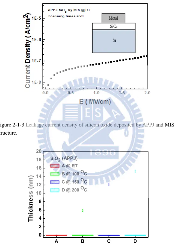
Figure 2-1-3 shows leakage current density of silicon oxide deposited by APPJ. The leakage current density of silicon oxide deposited by APPJ (APPJ-SiO2) is about
5E-7 A/cm2 at E = 0.5 MV/cm. However, the deposition rate at room temperature for APPJ-SiO2 insulator on aluminum electrode is almost zero, possibly ascribed to poor
chemical reaction rate on aluminum substrate. As we known, the surface active energy is highly related to substrate temperature based on chemical vapor deposition dynamics. The equation of chemical reaction rate was shown in Eq. (2-1).
) / exp( . .R A E kT C a (2-1)
24
Boltzmann constant. According to chemical reaction mechanism, the surface reaction can occur easily for the case with a low active energy. Therefore, we can choose different material with a low active energy or lower the reaction barrier by increasing substrate temperature to improve the deposition quality. Here, the different metals including Ni, Ti, Ta, Pt, and Pd have been applied to be the bottom electrode of the MIM capacitor, but the deposition rate of SiO2 (APPJ) at room temperature is still
poor, close to zero. We also used different metal oxide (HfO2, AlO2O3) as the buffered
materials between SiO2/electrode to decrease the active energy. However, the
deposition quality is still poor.
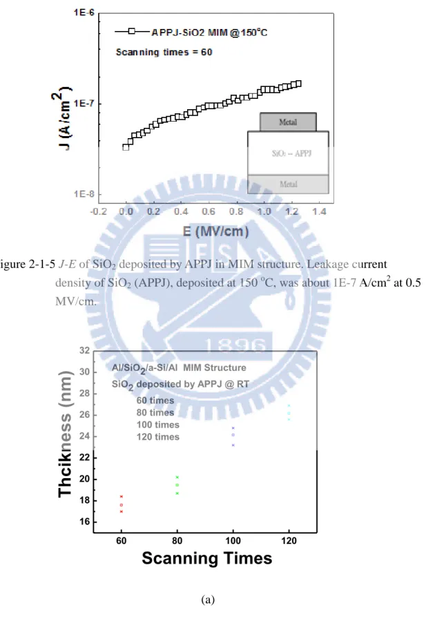
To deposit silicon oxide on the metal by APPJ, we tried to increase the substrate temperature up to 100 oC, 150 oC, and 200 oC. We used aluminum as the bottom electrode for MIM structure. Figure 2-1-4 shows the thickness of APPJ-SiO2 at
different temperatures, indicating deposition rate increased with substrate temperature, like surface reaction control. To clarify the effect of temperature-dependence deposition, a fixed flow rate of 200 sccm was applied to concise our experiment design. The detail discussion on the influence of flow rate would be investigated in next section. Figure 2-1-5 shows the leakage current density of silicon oxide deposited by E-gun and APPJ, respectively. The optimized APPJ-SiO2 at 150C
presents a leakage current density of 1E-7 A/cm2 at 0.5 MV/cm, much better than the silicon oxide deposited by E-gun with a leakage current of 4E-6 A/cm2.
However, the SiO2 deposition at room temperature is the future demand. The
improvement of surface reaction between Si and bottom electrode is crucial important. Therefore, we deposited silicon oxide on Al electrode with an amorphous Si buffered layer at room temperature. Figure 2-1-6(a) and (b) show C-V and I-V characteristics of Al/SiO2/amorphous Si/Al MIM structure, respectively. The good capacitance and
25
stable APPJ deposition process and reliable film quality. However, the experiment confirmed that the APPJ-SiO2 film could be deposited on a-Si and SiO2 substrate at
room temperature since the active energy of a-Si and SiO2 were lower than other
materials. The experimental results support our previous assumption, which a lower surface active energy facilitate APPJ-SiO2 deposition on Al electrode. As we
mentioned before, the higher thermal budget and Si buffered layer can deposit SiO2
successfully on Al electrode at room temperature, but the approach aided by buffered layer could increase the thickness variability and process complexity except for extra cost. In addition, we emphasized the importance of process temperature, since most plastic substrates could not sustain the temperature higher than 200 oC. The APPJ processed SiO2 at 150 oC not only maintains a good deposition rate for throughput but
also presents a good film quality which show the potential for low-temperature flexible electronic device fabrication.
After the above discussion, we have proposed approaches by using lower temperature control (<150C) and Si buffered layer to solve the issue of film deposition. Sequentially, the transistor characteristics will be discussed in the following part.
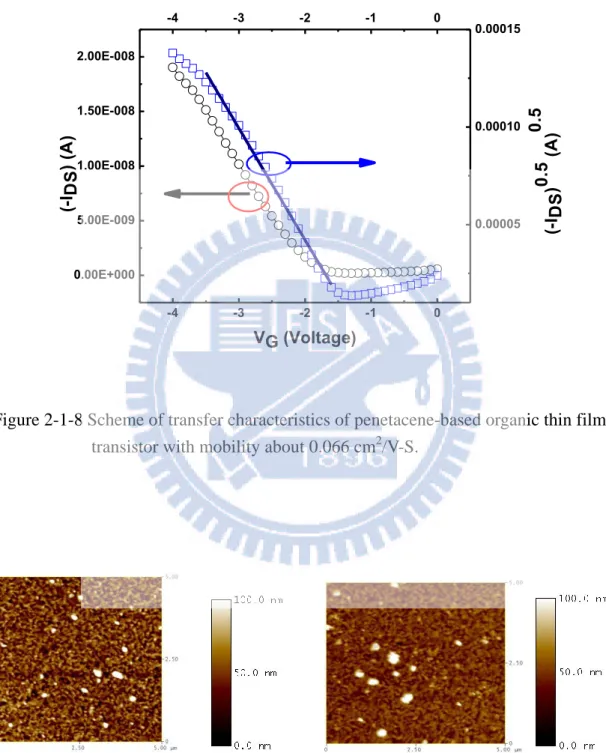
The drain current (ID) versus drain-source voltage (VDS) at varied gate voltages
(VGS) shown in Figure 2-1-7. The output characteristic of ID versus VGS was shown in
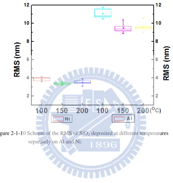
Figure 2-1-8. The carrier mobility at the saturation region was calculated by the equation:
ID
W C i/2L
(VG VT)2, [2]Ci is the capacitance per unit area of gate insulator in Eq (2). It correspond to a device with channel width W = 200 μm and length L = 100 μm.
26
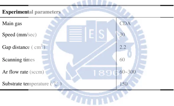
The operational voltage was below -4 V for a EOT of 12.4 nm. The saturation mobility and the threshold voltage of the OTFT were about 0.066 cm2 V-1s-1 and – 1.8 V, respectively. There are three possible reasons to explain why the mobility lower than pervious researches [14]-[17]. First, the grain size of the active layer would be affected by the roughness of the electrodes of source and drain due to bottom contact TFT structure. Secondly, poor oxide surface roughness could lead to the mobility degradation. In Figure 2-1-9, the roughness (RMS) of Al gate electrode was about 8.2 nm and a large RMS value of ~10.8 nm can be obtain after APPJ-SiO2 on the aluminum electrode. The uneven Al electrode could affect the roughness of following APPJ-SiO2. The contact angle of about 25 degree for APPJ-SiO2, showing hydrophilic characteristic on the oxide surface is another issue since the surface roughness and hydrophilic characteristics should be the main factors to influence the deposition of pentacene and then decrease the mobility of OTFT devices. To improve these issues, originated from bottom electrode with larger leakage current, we replaced Al (4.2eV) electrode by a higher work function Ni (5.1eV). Figure 2-1-10 shows the RMS of silicon oxide deposited at different temperatures on Al and Ni, respectively. The oxide on an evaporated Ni by E-gun has a RMS value of 2.2 nm, lower than that on Al. To reduce surface roughness of gate insulator and improve the gate leakage current, we used Ni as the bottom electrode of OTFT in the following experiment.
27 Silicon substrate Silicon dioxide electrode SAPPT silicon oxide Metal Insulator Metal
Figure 2-1-1 MIM structure for testing gate insulator’s quality.
50 nm Ni 50 nm Ni Silicon substrate 500 nm Thermal oxide 100 nm Al 12.4 nm silicon oxide 50 nm pentacene
28
Figure 2-1-3 Leakage current density of silicon oxide deposited by APPJ and MIS structure.
Figure 2-1-4 Thickness of silicon oxide with 60 times at different temperatures.
A B C D 0 2 4 6 8 10 12 14 16 18 20
T
h
ic
k
n
e
s
s
(
n
m
)
SiO2 (APPJ) A @ RT B @ 100 OC C @ 150 OC D @ 200 OC29
Figure 2-1-5 J-E of SiO2 deposited by APPJ in MIM structure. Leakage current
density of SiO2 (APPJ), deposited at 150 oC, was about 1E-7 A/cm2 at 0.5
MV/cm. (a) 60 80 100 120 16 18 20 22 24 26 28 30 32
Scanning Times
T
h
c
ik
n
e
s
s
(
n
m
)
Al/SiO2/a-Si/Al MIM Structure SiO2 deposited by APPJ @ RT60 times 80 times 100 times 120 times
30
(b)
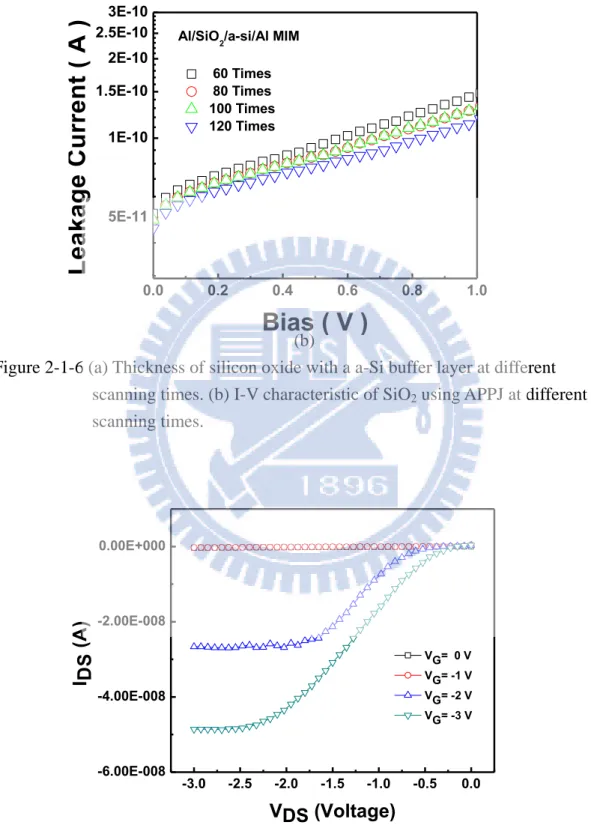
Figure 2-1-6 (a) Thickness of silicon oxide with a a-Si buffer layer at different scanning times. (b) I-V characteristic of SiO2 using APPJ at different
scanning times. -3.0 -2.5 -2.0 -1.5 -1.0 -0.5 0.0 -6.00E-008 -4.00E-008 -2.00E-008 0.00E+000 I DS ( A ) VDS (Voltage) VG= 0 V VG= -1 V VG= -2 V VG= -3 V
Figure 2-1-7 Scheme of the output characteristics of pentacene-based organic thin film transistor with a lower operation voltage about -3 V.
0.0 0.2 0.4 0.6 0.8 1.0 5E-11 1E-10 1.5E-10 2E-10 2.5E-10 3E-10
Al/SiO2/a-si/Al MIM 60 Times 80 Times 100 Times 120 Times
L
e
a
k
a
g
e
C
u
rr
e
n
t
(
A
)
Bias ( V )
31 -4 -3 -2 -1 0 0.00E+000 5.00E-009 1.00E-008 1.50E-008 2.00E-008 (-IDS ) 0 .5 ( A ) 0 .5 (-IDS ) (A ) VG (Voltage) -4 -3 -2 -1 0 0.00005 0.00010 0.00015
Figure 2-1-8 Scheme of transfer characteristics of penetacene-based organic thin film transistor with mobility about 0.066 cm2/V-S.
Figure 2-1-9 (a) AFM image of aluminum gate electrode with roughness about 8.7 nm.(b) AFM image silicon oxide (APPJ) deposited at 150 ℃ on the aluminum with the roughness around 10.8 nm
32
Figure 2-1-10 Scheme of the RMS of SiO2 deposited at different temperatures
separately on Al and Ni.
33
References
[1] S. E. Babayan, J. Y. Jeong, V. J. Tu, J. Park, G. S. Selwyn, and R. F. Hicks, “Deposition of silicon dioxide films with an atmospheric-pressure plasma jet,” Plasma Sources Sci. Technol., vol. 7, pp. 286-288, 1998.
[2] A. Ladwig, S. Babayan, M. Smith, M. Hester, W. Highland, R. Koch, R. Hicks, “Atmospheric plasma deposition of glass coatings on aluminum,” Surface &
Coatings Technology, vol. 201, pp. 6460-6464, 2007.
[3] G. R. Nowling, M. Yajima, S. E. Babayan, M. Moravej, X. Yang, W. Hoffman, and R. F. Hicks, “Chamberless plasma deposition of glass coatings on plastic,” Plasma Sources Sci. Technol. vol. 14, pp.477-484, 2005.
[4] J. Y. Jeong, S. E. Babayan, A. Schu¨ tze, V. J. Tu, and R. F. Hicks, “Etching polyimide with a nonequilibrium atmospheric-pressure plasma jet,” J. Vac. Sci. Technol. A, vol. 17, no. 5, 1999.
[5] K. Maruyama, I . Tsumagari, M. Kanezawa, Y. Gunji, M. Morita, M. Kogoma, and S. Okazaki, “Preparation of ZnO films from Zn2+ aqueous mist using atmospheric pressure glow plasma,” J. Mater. Sci. Lett. vol. 20, pp. 481-484, 2001.
34
2-2 The Effect Carrier Gas’s Flow Rate on The Surface Morphology and Film Quality
Carrier gas’s flow rate may be an influence factor for depositing SiO2, discussed
in many studies. In APPJ, flow rate would alter the concentration of the precursor at nozzle, influencing the deposition rate and the quality of silicon oxide. In this part, bubble method was utilized to carry the precursor into the plasma region and Ar was used as the carrier gas. The experimental detail was shown in Table 2-2-1. We selected substrate temperature at 150 ℃ because every experimental parameter must be suitable for plastic substrate. From Figure 2-2-1, we could obviously found that the leakage current density was increased with increasing the carrier gas’s flow rate. When the gas flow rate was less than 100 sccm, the leakage current density could be suppressed below 2 E-8 A/cm2 at 0.5 MV/cm. However, a larger leakage current of two order of magnitude (1E-6 A/cm2) than optimized one was obtained as introducing an excess follow rate of > 200 sccm. From Figure 2-2-2, the thickness and roughness were increased with increasing the flow rate of carrier gas. The AFM plots of SiO2
were also shown in Figure 2-2-3. The roughness of silicon oxide increased rapidly when the flow rate over 200 sccm. The rapid deposition rate would cause silicon oxide too loose to suppress leakage current. In addition, we used SEM to get the top view of silicon oxide surface shown in Figure 2-2-4 and found that these pellets on the silicon oxide surface was also increased obviously at higher flow rate. These pellets must be decreased because the surface roughness would scatter transport carriers which would decrease the mobility of OTFT. In addition, organic molecules
35
ordering and grain size would be degraded with high surface roughness [1-2] which would decrease the mobility of organic semiconductor. In our experiment, the roughness of silicon oxide could be reduced by decreasing the flow rate and the pellets also could be decreased, which would increase the possibility of application for OTFT. Figure 2-2-5 shows the XPS of silicon oxide deposited with different flow rates and the percentage of carbon existed in silicon oxide, shown in Table 2-2-2, was increased with increasing the flow rate. Some precursor may not be decomposed completely and then deposited on the surface of sample to form the impurities which may consist of C-H, C-O, and C-O-O in our demonstrated silicon oxide. This phenomenon may be more serious when the flow rate increases. CVD reactions are homogeneous, heterogeneous, or a combination of both. Homogeneous reactions nucleate in the gas phase and lead to particle formation. The greatest single problem in CVD technology. Most CVD processes are chosen to be heterogeneous reactions [3-4]. That is, they take place at the substrate surface rather than in the gas phase and form the desirable film deposit. In general, increasing temperature leads to increase film deposition rate, greater density, and improved structural perfection and crystallinity of the deposits. The quality of silicon oxide deposited by APPJ in this thesis was also improved with increasing temperature in lower flow rate. It is very important to control temperature and flow rate for depositing silicon oxide at heterogeneous reactions. Although silicon oxide deposited by APPJ in air may combined some particles or impurities, low leakage current density of insulator was obtained by well controlling temperature, flow rate, and other parameters of APPJ.
36
Table 2-2-1 The details of experimental parameters of silicon oxide deposited with different flow rates by APPJ.
Experimental parameters
Main gas CDA
Speed (mm/sec) 30
Gap distance ( cm2 ) 2.2
Scanning times 60
Ar flow rate (sccm) 60~300
37 0.0 0.5 1.0 1E-10 1E-9 1E-8 1E-7 1E-6 1E-5 1E-4 1E-3 0.01 J ( A /c m 2 ) E (MV/cm) 60 sccm 100 sccm 200 sccm 300 sccm 0.0 0.5 1.0
Figure 2-2-1 Plot of leakage current density versus electric field (J-E) of our APPJ- SiO2 deposited with different carrier gas’s flow rates.
50 100 150 200 250 300 0 10 20 30 40 50 60 70 80 90 100 110 Deposition rate D e p o s it io n r a te ( A 0 /m im -c m 2 ) Flow rate (sccm) 50 100 150 200 250 300 2 4 6 8 10 12 R M S ( n m ) RMS
Figure 2-2-2 Deposition rate and RMS of silicon oxide deposited with different flow rates of atmospheric pressure plasma jet.
38
(a) (b)
(c ) (d)
Figure 2-2-3 AFM images of silicon oxide fabricated with different Ar flow rates of APPJ. (a) 60 sccm (b) 100 sccm (c) 200 sccm (d) 300 sccm
39
(a) (b)
(c ) (d)
Figure 2-2-4 SEM images of silicon oxide fabricated with different Ar flow rates of atmospheric pressure plasma jet.
40
Figure 2-2-5 X-ray Photoelectron Spectroscopy spectra of SiO2 (APPJ) deposited with
different Ar flow rates.
Table 2-2-2 The concentration of carbon in silicon oxide, deposited with different flow rates, was analyzed by X-ray Photoelectron Spectroscopy.
5.87 9985.05 18142.94 1.71 6606.53 286.39 289.52 295.5 C1s 300sccm 4.52 7840.72 14248.2 1.96 5267.28 285.81 288.23 295.1 C1s 200sccm 4.1 6995.36 12710.8 2 5041.63 286.2 289.38 294.21 C1s 100sccm 3.81 6543.55 11891.34 1.99 4786.72 285.49 287.87 293.09 C1s 60sccm At. % Area (N) Area (P) CPS.eV FWHM eV Height Counts End BE Peak BE Start BE Name 5.87 9985.05 18142.94 1.71 6606.53 286.39 289.52 295.5 C1s 300sccm 4.52 7840.72 14248.2 1.96 5267.28 285.81 288.23 295.1 C1s 200sccm 4.1 6995.36 12710.8 2 5041.63 286.2 289.38 294.21 C1s 100sccm 3.81 6543.55 11891.34 1.99 4786.72 285.49 287.87 293.09 C1s 60sccm At. % Area (N) Area (P) CPS.eV FWHM eV Height Counts End BE Peak BE Start BE Name
41
Reference
[1] J. H. Seo, J. H. Kwon, and S. I. Shin, “Organic thin film transistors with polyvinyl alcohol treated dielectric surface,” Semiconductor Science and Technology, vol. 22, no. 9, pp. 1039-1043, Sep. 2007.
[2] W. H. Lee and C. C. Wang, “Effect of nanocomposite gate dielectric roughness on pentacene field-effect transistor,” J. Vac. Sci. Technol. B, vol. 27, no. 3, pp. 1116-1121, May 2009.
[3] K. J. Huttinger, “CVD in Hot Wall Reactors - The Interaction Between Homogeneous Gas-Phase and Heterogeneous Surface Reactions,” Chemical Vapor Deposition, vol. 4, no. 4, pp. 151-158, pp. JUN 1998.
[4] G. G. Condorelli, A. Baeri, I. L. Fragala, “Homogeneous and heterogeneous reactions in the decomposition of precursors for the MOCVD of high-k and ferroelectric films,” Materials Science in Semiconductor Processing, vol. 5, no. 2-3, pp. 135-139, Apr. Jun. 2002
[5] V. Nehra, A. Kumar,and H. K. Dwivedi, “Atmospheric Non-Thermal Plasma Sources,” International Journal of Engineering, vol. 2, no. 1, pp. 53-68,