sented by considering corner effects, short-channel effects, and channel-doping profiles. A novel TG MOSFET structure with a polysilicon gate process is proposed using asymmetrical (n+/p+) polysilicon gates. CMOS-compatible VT’s for high-performance
circuit applications can be achieved for both nFET and pFET. The superior subthreshold characteristics and device performance are analyzed and validated by 3-D numerical simulations. Com-parisons of device characteristics with a midgap metal gate are presented.
Index Terms—Corner effects, polysilicon gate, triple-gate (TG) MOSFETs.
I. INTRODUCTION
T
HE TRIPLE-GATE (TG) MOSFET (Fig. 1) has emerged as one of the promising candidates to extend CMOS technology beyond the scaling limit of conventional CMOS technology. The control of short-channel effects (SCEs) has become one of the major issues for device scaling beyond the 65-nm node [1]. Several emerging planar and nonplanar struc-tures that aimed to alleviate the SCEs have been proposed [1]. In these devices (e.g., fully depleted SOI MOSFETs, double-gate (DG) FinFETs, and TG MOSFETs), thin silicon film is usually required, yet challenging, to suppress the SCEs. The DG FinFET (with ultrathin fin) exhibits superior SCE control and current drive. On the other hand, the TG FET relaxes the requirements on fin height and fin (silicon film) thickness, thus allowing more flexible body dimension and fin aspect ratio to ease manufacturability [2]–[4].However, the mobile carrier density of the TG device is higher in the corner than the other portions of the channels at low gate voltage due to high electric field at sharp edges, which degrades the subthreshold slope. Furthermore, the corner
Manuscript received March 10, 2008; revised May 29, 2008. The work of M.-H. Chiang and J.-N. Lin was supported in part by the National Science Council of Taiwan, R.O.C., under Contract NSC-96-2221-E-197-023. The work of K. Kim and C. T. Chuang was supported in part by DARPA under Contracts NBCH30390004 and BGR W0132280. The review of this paper was arranged by Editor M. J. Kumar.
M.-H. Chiang is with the Department of Electronic Engineering, Na-tional Ilan University, I-Lan 260, Taiwan, R.O.C. (e-mail: mhchiang@ niu.edu.tw).
J.-N. Lin was with the Department of Electronic Engineering, National Ilan University, I-Lan 260, Taiwan, R.O.C. He is now with the Taiwan Army, Taipei, Taiwan, R.O.C.
K. Kim is with the VLSI Design Department, IBM T. J. Watson Research Center, Yorktown Heights, NY 10598 USA.
C.-T. Chuang is with the Department of Electronic Engineering, National Chiao-Tung University, Hsinchu 30050, Taiwan, R.O.C.
Color versions of one or more of the figures in this paper are available online at http://ieeexplore.ieee.org.
Digital Object Identifier 10.1109/TED.2008.927664
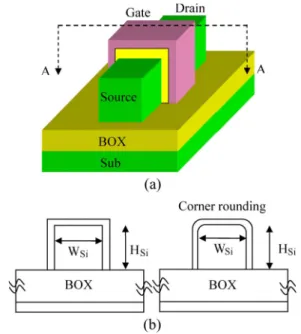
Fig. 1. (a) Three-dimensional TG structure (not to scale). (b) Two-dimensional cross sections (A−A) of the TG device with rectangular and rounded corners.
effects are more significant at high channel doping levels, thus directly affecting the device profile design [3], [5], [6]. As a result, low doping levels would seem to be a natural solution. Thus, conventional technique using channel doping to adjust the threshold voltage (VT) could be limited. In fact, metal
gates with proper work functions, instead of channel doping engineering, have been employed to achieve the desired VT in
advanced multigate structures [7]–[9]. For CMOS application, two different work functions are usually required in order to balance the drive currents of nFET and pFET, which leads to technology complexity. In addition, gate work function engineering for multi-VT design requires more exotic gate
materials.
In this paper, we present pragmatic TG device design consid-erations with emphasis on the feasibility of polysilicon gate and the choice of nonrectangular body structure while accounting for the noted corner effects using 3-D numerical simulations [10]. In the simulations, Fermi–Dirac statistics, modified lo-cal density approximation for carrier confinement, and drift-diffusion transport model with field-dependent mobility are used. Impacts of corner rounding and body-doping profiles on SCEs and other device characteristics are investigated. We also compare the nonrectangular structures with the ideal case of rectangular corners. Another challenging task for the multigate
curvature (HSi= 25 nm, WSi= 25 nm, and L(effective) = 25 nm).
technology development is the gate engineering for setting proper VT. To facilitate the use of polysilicon gate material,
we propose an asymmetrical (n+/p+) poly-gate structure for TG FinFET devices with CMOS-compatible VT’s using tilted
implantations [11], [12]. Note that in [12], tilted implantations have been employed to the fabrication of asymmetrical DG FinFET devices with CMOS-compatible VT’s. In the following
sections, the device characteristics of the proposed structure are comprehensively analyzed. Comparisons of device characteris-tics with a midgap metal gate are presented.
II. CONVENTIONALDEVICESTRUCTURE
WITHMIDGAPGATE
The device structure under study (Fig. 1), with midgap gate, has a cross-sectional body dimension of HSi= 25 nm and WSi= 25 nm, L(effective) = 25 nm, gate-oxide thickness (physical) = 1 nm, and buried oxide thickness = 200 nm. We first examine the control of SCEs via doping profile design with corner-rounding effects. Fig. 2 shows DIBL versus body doping for different radii of corner curvature r for the top corners. Due to higher transverse electric field at sharp edges of the ideal rectangular case, implying better SCE control, it shows slightly lower DIBL than the nonrectangular case (e.g., DIBL = 154 and 161 mV/V for r = 0 (ideal) and 5 nm, respectively, at Na = 5× 1018 cm−3), but the difference is insignificant.
The noncritical effect of corner rounding on SCE eases the rectangular body requirement in TG technology. However, very high doping appears necessary in order to suppress DIBL (< 100 mV/V). This is technologically challenging, and the performance tradeoff requires thorough study, as the silicon body could become partially depleted, causing floating-body effects, and the junction tunneling leakage could also become an issue at high body doping.
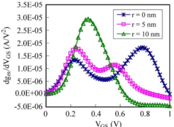
Fig. 3 shows the impact of corner rounding at very high doping (Na= 3× 1019 cm−3) on gm variations. Evidently,
the bimodal (two peaks) behavior reveals the two distinct VT’s
associated with the corners and the top/sidewalls, respectively. The corners, corresponding to the first peak, turn on earlier due to high electric fields at sharp edges. For nonrectangular case (r = 5 nm), the two peaks are closer since the sharp-edge effects are alleviated. As shown in Fig. 4(a) (r = 5 nm), the corner conduction is not as predominant since electron concentration is well distributed around the rounded corners
curvature at Na= 3× 1019cm−3(V
DS= 0.05 V)(HSi= 25 nm, WSi= 25 nm, and L(effective) = 25 nm).
instead of crowded at sharp edges. For the near-cylindrical case (r = 10 nm), the sharp-edge effects almost diminish com-pletely. For moderately high Na(5× 1018cm−3), the bimodal
behavior in VT virtually disappears as the electron density
is quite uniform around the corners, top, and sidewalls, as shown in Fig. 4(b), where the three sides of the gate conduct simultaneously.
Due to technology simplicity, the TG device with undoped or lightly doped body is preferred. Nonetheless, in this case, the DIBL would be unacceptably high with the same device size used for high body doping. Rather than adjusting the doping, ratios of WSi and HSi to channel length must be reduced to achieve good SCEs [3]. Here, we reduce WSiand HSito half of the channel length for proper DIBL (73 mV/V).
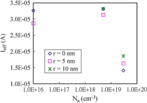
Due to different inversion conditions for heavily doped body and lightly doped body, device structure with corner rounding can be optimized to improve performance. In the subthreshold regime, the lightly doped case is predominantly affected by volume inversion, whereas corner inversion is the main con-tribution to Ioff for the heavily doped case. Therefore, corner rounding has very little impact on Ioff for devices with lightly doped body. In strong inversion, corner and edge inversions become more significant regardless of body doping, and hence, the shape of corners will have an impact on Ion. Fig. 5 shows Ieff (the effective current during switching [13]) versus body doping for different radii of corner curvature. For the very high Na, we observe that Ieff increases with r due to additional top/sidewall conduction in strong inversion regime as the second peak (top/sidewall conduction) in Fig. 3 moves toward lower VGS and eventually merges with the first peak (corner conduction). As a result, all edges, top, and sidewalls conduct simultaneously, resulting in a higher current. Thus, semicylindrical (tubelike) body would be preferable to improve performance without the sharp-edge effects. Note that since the body dimension of the low Na(1× 1016cm−3) case is half that
of the other two higher Nacases, it has the highest effective Ion per unit device width and the best CV /I due to inherent advan-tages such as higher mobility and steeper subthreshold slope from gate-to-gate capacitive coupling. Volume inversion also improves the subthreshold slope (the benefit reduces as doping increases). Contrary to the heavily doped case, the rectangular corners (r = 0 nm) seem advantageous to Ionfor the low Na
Fig. 4. Simulated electron density in the channel (cut at the midpoint between source and drain) for r = 5 nm at (a) Na= 3× 1019 cm−3 and (b) Na= 5× 1018cm−3(V
GS= 1.0 V and VDS= 0.05 V) (HSi= 25 nm, WSi= 25 nm, and L(effective) = 25 nm).
Fig. 5. Predicted Ieff versus body doping for different radii of corner cur-vature with comparable Ioff for all cases where Ieff= [(IDS at VGS=
VDD and VDS= VDD/2)+(IDS at VDS= VDD and VGS= VDD/2)]/2 [13]. Because r = 10 nm is too large for reduced WSi and HSi at Na= 1× 1016cm−3, it is not included.
inversion and introduce additional corner conduction in strong inversion.
III. PROPOSEDDEVICESTRUCTURE
A novel TG FinFET structure compatible with the polysil-icon process is proposed. Although the lightly doped channel seems to be a viable option and even preferable due to doping-dependent mobility, it is limited to the availability of midgap gates for CMOS application. In the conventional dual polysil-icon CMOS technology (i.e., n+and p+ polysilicon for nFET and pFET, respectively), the required channel doping density for TG devices has to be extremely high to achieve proper VT
(∼0.2 V) and, hence, Ioff (100 nA/µm), as shown in Fig. 6. The proposed TG device structure with physically equivalent n+- and p+-polysilicon gates is shown in Fig. 7(a). Two other possible structures with n+/p+ polysilicon gate offsets are shown in Fig. 7(b) and (c). The gate oxide surrounded by the gate has a uniform thickness (Tox). The device structure under study has a cross-sectional body dimension of height (HSi) and width (WSi). HSi and WSi are assumed to be equal and are half of the effective channel length for proper SCE control. The total channel width can be defined as 2H + W . Multi-VT
options can be achieved using different patterns of the n+/p+ polysilicon. It is worth noting that as high-k metal gates are
Fig. 6. Taurus-simulated IDS versus VGS characteristics for a TG nMOSFET with n+ polysilicon gate and different dopings (Na’s) (L = 25 nm, gate oxide = 1.3 nm, and silicon height = silicon width = 12.5 nm).
Fig. 7. Three-dimensional view of the proposed TG structures (a), (b), and (c) with different n+/p+polysilicon gate offsets. The thick BOX layer underneath is not shown.
used in planar CMOS technologies from the 45-nm node, the possible difficulty in high-k integration with polysilicon gates and random dopant fluctuation, although not included in this paper, could be potential issues to be resolved for polysilicon gates to remain viable as semiconductor technology advances.
We first assess the device I–V characteristics for the three gate structures, as compared with a midgap metal-gate device using 3-D numerical simulations [10]. All devices (nFETs) have the same L of 25 nm, Toxof 1.3 nm, and thick buried oxide (BOX) of 200 nm. Fig. 8 shows the simulated IDSversus VGS characteristics for the proposed structure (a) and the midgap metal-gate device with comparable Ioff(∼50 nA/µm) set at
Fig. 8. Taurus-simulated IDS versus VGS characteristics for the pro-posed structure (a) and the midgap metal-gate device with comparable
Ioff(∼50 nA/µm) set at VDS= 1.1 V.
Fig. 9. Taurus-simulated IDSversus VGScharacteristics for the three pro-posed structures.
VDS= 1.1 V. To achieve equal Ioff value, a channel doping density of 7× 1018cm−3is needed for the proposed structure, whereas an undoped body is used for the near-midgap metal-gate device. Due to higher mobility in the undoped channel, the midgap metal-gate device gives higher Ion (at VGS= VDS= 1.1 V). On the other hand, the proposed device exhibits better DIBL characteristics due to the higher vertical field attained by the positive back-gate field in the asymmetrical device configuration as well as the use of the doped body. Fig. 9 shows the simulated IDSversus VGScharacteristics for the three cases with different n+/p+ polysilicon gate offsets, as shown in Fig. 7. The same channel doping density (7× 1018cm−3) is used. Case (b) with larger p+-polysilicon portion has the highest VT, whereas case (c) with larger n+-polysilicon
por-tion has the lowest VT. Fig. 10 further shows the Ion versus
Ioff characteristics for the three poly-gate and the metal-gate devices. The three proposed structures offer a wide range of
VT selection; thus, multiple VT’s can be made. Note that for
the DG FinFET structure, the proposed multi-VT technique via
partitioned n+/p+ polysilicon on the top gate would not be practical because the top-gate area of FinFET is too narrow and, thus, ineffective.
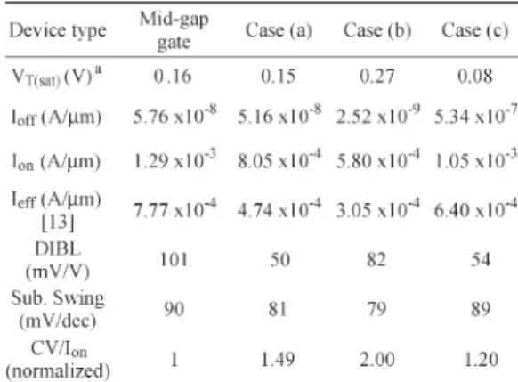
The detailed device characteristics are listed in Table I (VDD= 1.1 V). The proposed structures have lower DIBL and better subthreshold slope compared with the metal-gate device. Fig. 11 shows the inversion carrier distribution in the channel. The electron density is more uniformly distributed for the midgap metal-gate device, whereas it is crowded near
metal-gate device.
TABLE I
PREDICTEDDEVICECHARACTERISTICS OF THEPROPOSEDSTRUCTURES AND THEMIDGAPMETAL-GATEDEVICE FORCOMPARISON
Fig. 11. Electron distribution in the cross-sectional cut at midchannel for (a) the midgap metal-gate device and (b) the proposed structure (a) (VGS=
VDS= 0 V).
the n+-gate surface for the proposed structure (a) (results for structures (b) and (c) are not shown, yet similar). Hence, the proposed structures have improved DIBLs, as the carriers are better controlled due to the higher field perpendicular to the predominant n+gate.
Fig. 12 shows the Ion and Ioff sensitivities to VDD. As expected, Ioff for structure (a) is slightly less sensitive than that for the midgap metal-gate device due to less DIBL. The
Ion dependences on VDD are similar for the three proposed structures, implying consistent dynamic power scaling when these structures are integrated on the same chip for multi-VT
design. The DIBL advantage is further shown in Fig. 13. To gain insight into CMOS circuit speed performance, we also
Fig. 12. Predicted Ionand Ioffsensitivities to VDD.
Fig. 13. Predicted VT(sat)and DIBL versus L scaling.
Fig. 14. Predicted C–V characteristics.
simulated C–V characteristics, as shown in Fig. 14, for CV /I comparison. The CV /Ion value of our proposed structure [case (a)] is about 50% (at VDDof 1.1 V) higher than that of the midgap metal-gate device mainly due to lower Ion. However, as
VDDis decreased, the gate capacitance for the proposed scheme decreases faster, and hence, it is more suitable for low-voltage applications. Overall, while the CV and IV performances of the proposed structure are not superior partly due to lower
structure is preferable for heavily doped devices, whereas rec-tangular gate structure appears better for lightly doped devices. A novel TG MOSFET structure using asymmetrical polysil-icon gates is proposed. Due to the superior SCEs, the pro-posed TG device offers better channel length scalability compared with the TG devices with near-midgap metal gates. By changing the patterns/offsets of the n+/p+ polysilicon gates, multiple VT’s can be achieved, thus making it attractive
for low-power high-performance very large scale integration applications.
REFERENCES
[1] International Technology Roadmap for Semiconductors, 2004. [Online]. Available: http://public.itrs.net/
[2] B. Doyle, B. Boyanov, S. Datta, M. Doczy, S. Hareland, B. Jin, J. Kavalieros, T. Linton, R. Rios, and R. Chau, “Tri-gate fully-depleted CMOS transistors: Fabrication, design and layout,” in VLSI Symp.Tech.
Dig., 2003, pp. 133–134.
[3] J.-W. Yang and J. G. Fossum, “On the feasibility of nanoscale triple-gate CMOS transistors,” IEEE Trans. Electron Devices, vol. 52, no. 6, pp. 1159–1164, Jun. 2005.
[4] J. Kavalieros, B. Doyle, S. Datta, G. Dewey, M. Doczy, B. Jin, D. Lionberger, M. Metz, W. Rachmady, M. Radosavljevic, U. Shah, N. Zelick, and R. Chau, “Tri-gate transistor architecture with high-k gate dielectrics, metal gates and strain engineering,” in VLSI Symp. Tech. Dig., 2006, pp. 50–51.
[5] W. Xiong, J. W. Park, and J. P. Colinge, “Corner effect in multiple-gate SOI MOSFETs,” in Proc. IEEE Int. SOI Conf., 2003, pp. 111–113. [6] J. G. Fossum, J.-W. Yang, and V. P. Trivedi, “Suppression of corner effects
in triple-gate MOSFETs,” IEEE Electron Device Lett., vol. 24, pp. 745– 747, 2003.
[7] J. Kedzierski, E. Nowak, T. Kanarsky, Y. Zhang, D. Boyd, R. Carruthers, C. Cabral, R. Amos, C. Lavoie, R. Roy, J. Newbury, E. Sullivan, J. Benedict, P. Saunders, K. Wong, D. Canaperi, M. Krishnan, K.-L. Lee, B. A. Rainey, D. Fried, P. Cottrell, H.-S. P. Wong, M. Ieong, and W. Haensch, “Metal-gate FinFET and fully-depleted SOI devices using total gate silicidation,” in IEDM
Tech. Dig., Dec. 2002, pp. 247–250.
[8] Y. K. Choi, L. Chang, P. Ranade, J.-S. Lee, D. Ha, S. Balasubramanian, A. Agarwal, M. Ameen, T-J. King, and J. Bokor, “FinFET process re-finements for improved mobility and gate workfunction engineering,” in
IEDM Tech. Dig., Dec. 2002, pp. 259–262.
[9] J. Kedzierski, M. Ieong, T. Kanarsky, Y. Zhang, and H.-S. P. Wong, “Fabrication of metal gated FinFETs through complete gate silicidation with Ni,” IEEE Trans. Electron Devices, vol. 51, no. 12, pp. 2115–2120, Dec. 2004.
[10] Taurus-Device, User Guide, Synopsis Inc. ver. X-2005.10, Oct. 2005. [11] K. Kim and J. G. Fossum, “Double-gate CMOS: Symmetrical- versus
asymmetrical-gate devices,” IEEE Trans. Electron Devices, vol. 48, no. 2, pp. 294–299, Feb. 2001.
[12] J. Kedzierski, D. M. Fried, E. J. Nowak, T. Kanarsky, J. H. Rankin, H. Hanafi, W. Natzle, D. Boyd, Y. Zhang, R. A. Roy, J. Newbury, C. Yu, Q. Yang, P. Saunders, C. P. Willets, A. Johnson, S. P. Cole, H. E. Young, N. Carpenter, D. Rakowski, B. A. Rainey, P. E. Cottrell, M. Ieong, and H-S. P. Wong, “High-performance symmetric-gate and CMOS-compatible Vt asymmetric FinFET devices,” in IEDM Tech. Dig., Dec. 2001, pp. 437–440.
[13] M. H. Na, E. J. Nowak, W. Haensch, and J. Cai, “The effective drive current in CMOS inverters,” in IEDM Tech. Dig., 2002, pp. 121–124.
Jeng-Nan Lin received the B.S. and M.S. degrees in
electronic engineering from the National Ilan Uni-versity, I-Lan, Taiwan, R.O.C., in 2005 and 2007, respectively. His thesis was focused on advanced semiconductor device modeling and simulation.
He is currently with the Taiwan Army, Taipei, Taiwan, R.O.C., for mandatory military service.
Keunwoo Kim (S’98–M’01–SM’06) was born in
Daegu, Korea, in 1968. He received the B.S. degree in physics from Sungkyunkwan University, Seoul, Korea, in 1993, and the M.S. and Ph.D. degrees in electrical and computer engineering from the Uni-versity of Florida, Gainesville, in 1998 and 2001, respectively. His doctoral research was in the area of SOI and double-gate (DG) device design and modeling.
Since June 2001, he has been a Research Staff Member with the VLSI Design Department, IBM T. J. Watson Research Center, Yorktown Heights, NY. He has worked on the design of high-performance and low-power microprocessors, novel very large scale integration circuit techniques, scaled and exploratory CMOS technol-ogy performance/power evaluation, and physics/modeling for bulk-Si, SOI, strained-Si, SiGe, hybrid orientation/device, and DG technologies. He has published over 70 papers in technical journals and conference proceedings. He is the holder of seven U.S. patents with another ten pending U.S. patents. His present work includes IBM’s POWER7 processor design, the analysis and prediction of SRAM variability/yields, and system-level performance/power projections.
Dr. Kim has been a Reviewer of the journal publications for the IEEE TRANSACTIONS ON ELECTRON DEVICES, the IEEE TRANSACTIONS ON
COMPUTER-AIDEDDESIGN OFINTEGRATEDCIRCUITS ANDSYSTEMS, the IEEE TRANSACTIONS ONVERYLARGESCALEINTEGRATIONSYSTEMS, and the Solid-State Electronics. He was the recipient of five invention achieve-ment awards from IBM. He was listed in Who’s Who in America (2007 Edition).
speed high-density bipolar SRAMs, multigigabit-per-second fiber-optic data-link circuits, and scaling issues for bipolar/BiCMOS devices and circuits. Since 1988, he has been managing the High Performance Circuit Group, investigating high-performance logic and memory circuits. Since 1993, his group has been primarily responsible for the circuit design of IBM’s high-performance CMOS microprocessors for enterprise servers, PowerPC workstations, and game/media processors. Since 1996, he has been leading the efforts in evaluating and exploring scaled/emerging technologies, such as PD/SOI, UT/SOI, strained-Si devices, hybrid orientation technology, and multigate/FinFET devices, for high-performance logic and SRAM applications. Since 1998, he has been responsible for the Research VLSI Technology Circuit Co-design strategy and execution. His group has also been very active and visible in leakage/ variation/degradation tolerant circuit and SRAM design techniques. He took early retirement from IBM to join the National Chiao-Tung University, Hsinchu, Taiwan, where he has been a Chair Professor with the Department of Electronic Engineering since February 2008. He has authored many in-vited papers in international journals such as International Journal of High
Speed Electronics, PROCEEDINGS OFIEEE, IEEE Circuits and Devices
Mag-azine, and Microelectronics Journal. He has also authored or coauthored over
260 papers. He is the holder of 27 U.S. patents with another 14 pending. Dr. Chuang was elected as an IEEE Fellow in 1994 “for his contribu-tions to high-performance bipolar devices, circuits, and technology.” He has presented numerous plenary, invited, or tutorial papers/talks at international conferences such as International SOI Conference, DAC, VLSI-TSA, ISSCC Microprocessor Design Workshop, VLSI Circuit Symposium Short Course, ISQED, ICCAD, APMC, VLSI-DAT, ISCAS, MTDT, WSEAS, etc. He served on the Device Technology Program Committee for IEDM in 1986 and 1987 and the Program Committee for Symposium on VLSI Circuits from 1992 to 2006. He was the Publication/Publicity Chairman for the Symposium on VLSI Technology and the Symposium on VLSI Circuits in 1993 and 1994, and the Best Student Paper Award Subcommittee Chairman for the Sym-posium on VLSI Circuits from 2004 to 2006. He was the corecipient of the Best Paper Award at the 2000 IEEE International SOI Conference. He has received one Outstanding Technical Achievement Award, one Research Division Outstanding Contribution Award, five Research Division Awards, and 12 Invention Achievement Awards from IBM. He has received the Outstanding Scholar Award from Taiwan’s Foundation for the Advancement of Outstanding Scholarship for 2008 to 2013.