國
立
交
通
大
學
電控工程研究所
碩
士
論
文
具虛擬斜坡電流平衡技術之電壓模式多相位降壓轉
換器
Pseudo-Ramp Current Balance (PRCB) Technique for
Voltage-Mode Multiphase Buck Converter
研究生:黃玉萍
指導教授:陳科宏 博士
具虛擬斜坡電流平衡技術之電壓模式多相位降壓轉換器
Pseudo-Ramp Current Balance (PRCB) Technique for Voltage-Mode
Multiphase Buck Converter
研 究 生:黃玉萍 Student:Yu-Ping Huang
指導教授:陳科宏 Advisor:Ke-Horng Chen
國 立 交 通 大 學
電 控 工 程 研 究 所
碩 士 論 文
A Thesis
Submitted to Institute of Electrical Control Engineering
College of Electrical and Computer Engineering
National Chiao Tung University
in partial Fulfillment of the Requirements
for the Degree of
Master
in
Electrical Control Engineering
September 2011
Hsinchu, Taiwan, Republic of China
中華民國一百年九月
i
具虛擬斜坡電流平衡技術之電壓模式多相位降壓轉換器
研究生:黃玉萍
指導教授:陳科宏博士
國立交通大學電控工程研究所碩士班
摘
要
在現今科技發展不斷進步的社會中,體積小且多功能的可攜式產品越來越受到歡迎, 例如智慧型手機、MP3 及平板電腦等設備。除了功能選項多能吸引消費者,這些可攜式 產品的操作時間是一個重要的考量;越長的操作時間表示系統越省電越不需要多次充電, 具有很大的方便性.為了設計出省電的系統,如何使電源系統具備高效率、低損耗的特 點是一項考驗,特別是需在可攜式產品有限的空間中設計。另外,在某些系統中,常常 會需要電源管理電路可以提供大電流、低電壓漣波等要求,如 CPU 的電源規格.在這樣 的情況下,多相位電源轉換器是一個很好的選擇。透過多相位的方式,並聯多組降壓或 升壓等電壓轉換 cell 以提供大電流到輸出端。但當相位越多,也就是並聯的組數越多, 就需要越多的控制器來對應多相位的控制。 為了解決多相位造成的多控制器之電源消耗與面積無法縮小問題,本論文提出一具 虛擬斜坡電流平衡技術應用於電壓模式多相位直流-直流降壓轉換器,只需使用一組控 制器即可達到多相位控制。在本論文中,將會依序介紹虛擬斜坡技術與對應的時間多功 電流平衡機制、系統穩定度分析、電路實現方法、電路量測結果與結論。
ii
Pseudo-Ramp Current Balance (PRCB) Technique for Voltage-Mode
Multiphase Buck Converter
Student: Yu-Ping Huang
Advisor: Dr. Ke-Horng Chen
Department of Electrical and Control Engineering
National Chiao-Tung University
ABSTRACT
A pseudo-ramp current balance (PRCB) technique is proposed to achieve the time-multiplexing (TM) current balance in voltage-mode multiphase DC-DC buck converter with only one modulation controller. Thus, compared to the conventional multiphase converter, the N-1 controllers can be removed when the PRCB technique is implemented in the monolithic N-phase DC-DC buck converters for largely decreasing the silicon area and power consumption. In addition, the TM current balance scheme can further enhance the current sharing accuracy since the mismatches between different controllers does not exist. Particularly, an explicit model of multiphase converter with the PRCB technique is derived for system stability analysis. Both of the voltage loop and the current balance loops with non-ideal effect are taken into consideration. Experimental results show that the current difference between each phase can be decreased by over 83 % at both heavy load and light load conditions.
iii
誌 謝
在本論文開始之前,感謝指導教授 陳科宏博士在我大學四年以及碩士兩年的照顧 與指導,從大學導師開始跟著老師學習電子學,到碩士指導教授跟著老師學習研究精神 與處事態度,多年的指導實在難以三兩文字敘述,但仍藉此誌謝表達感激之情。 另外,在實驗室兩年多的時間中,受到了許許多多人的幫助,特別是李昱輝博士班 學長。昱輝學長從大學營隊開始就一直是我的精神指標,到進了實驗室,更是亦師亦友 的存在,除了在研究方面給予了極大的教導與協助外,在日常生活中更是點滴在心。除 了昱輝學長,也要感謝俊禹學長、耀沂學長、梓期學長、契霖學長、緯權學長、士榮學 長、士偉學長、智宇學長、銘彥學長在前前後後兩年多的時間中的教導與幫助。此外, 感謝我的好夥伴以萍,從認識以來一直受到諸多照顧與幫忙,在以萍身上也學習到了很 多,每一項都是歷歷在目。還有,感謝同學淳仁、冠宇、雅萍、怡婷的照顧,讓碩士兩 年的時光過得很充實。另外,感謝瑋中、嘉隆、佑儕、之樸、俊彥、大龍在碩二的陪伴, 讓實驗室總是充滿了笑聲與歡樂,也感激一直以來的幫助與指教。 除了實驗室的學長同學,感謝我的好室友們:水滴、艷艷、小詩雯、阿紫的陪伴與 鼓勵,在研究挫折或壓力繁大時,你們的鼓勵一直都是我最大的感動與感謝。也感謝我 的家人,感謝爸爸媽媽從小到大的照顧,感謝姐姐妹妹弟弟在日常生活的關懷,你們永 遠是我最大的支持。 最後,對於本論文的完成,再次感謝昱輝學長與以萍同學,在事務繁忙之際,給予 我極大的幫助,實在萬分感激,沒齒難忘。也祝福你們在未來繼續的研究生涯順利成功。 玉萍 于 桂月 國立交通大學 中華民國一百年九月iv
Contents
Chapter 1 ... 1
Introduction ... 1
1.1 Background of Power Management System and Voltage Regulators ... 1
1.2 Classification of Voltage Regulators ... 2
1.2.1 Linear Regulator ... 2
1.2.2 Switching Capacitor Regulator ... 4
1.2.3 Switching Regulators ... 5
1.3 Design Motivation ... 7
1.4 Thesis Organization ... 9
Chapter 2 ... 10
Proposed Multiphase Structure and the PRCB Operation Principle ... 10
2.1 System Operation ... 10
2.1.1 Pseudo-Ramp Operation ... 12
2.1.2 Time-Multiplexing Current Balance Mechanism ... 15
2.2 Stability Analysis of the Multiphase Converter with the PRCB Technique ... 16
2.2.1 The Model of the Pseudo-Ramp Technique ... 17
2.2.2 TM Current Balance Model ... 18
2.2.3 System Stability Analysis ... 21
Chapter 3 ... 26
Circuit Implementation ... 26
3.1 Current Sensing Circuit ... 26
3.2 Current Balance Circuit ... 27
3.3 Pseudo-Ramp Generator ... 28
3.4 Phase Control Logic ... 30
Chapter 4 ... 33
Experimental Results ... 33
4.1 Chip Micrograph and Design Specification ... 33
4.2 Steady-State Operation Results ... 34
4.3 Load Transient Response ... 35
4.4 Line Transient Response ... 37
4.5 Current Balance Performance Analysis ... 38
4.6 Power Conversion Efficiency ... 39
Chapter 5 ... 40
v
5.1 Conclusion ... 40 5.2 Future Work ... 41 References ... 42
vi
Figure Captions
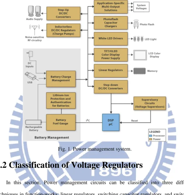
Fig. 1. Power management system. ... 2
Fig. 2. The schematic of a low drop-out regulator. ... 3
Fig. 3. The schematic of a switching capacitor regulator. ... 4
Fig. 4. The simple architecture of buck converter. ... 5
Fig. 5. Conventional structure of the N-phase voltage-mode DC-DC buck converter. ... 8
Fig. 6. Structure of the N-phase DC-DC buck converter with proposed PRCB technique. ... 11
Fig. 7. The illustration of the PRCB technique in the Mode I and the Mode II. ... 13
Fig. 8. The timing diagrams when the DBP is utilized. ... 14
Fig. 9. Current balance mechanism implemented with pseudo-ramp operation in the proposed dual-phase DC-DC buck converter. ... 16
Fig. 10. Equivalent model of the two-phase converter with the pseudo-ramp technique. ... 17
Fig. 11. (a) Equivalent model of the pulse-width modulator with the current balance. (b) The relationship between the duty cycle and the adjusted ramp. ... 19
Fig. 12. Equivalent model of dual-phase buck converter with the PRCB technique and the TM current balance. ... 22
Fig. 13. Small signal model of the TM current balance loop. ... 23
Fig. 14. The frequency response of the Tv(s), the Tcb(s) and the Tcc(s)... 24
Fig. 15. The current sensing circuit. ... 27
Fig. 16. Current balance circuit. ... 28
Fig. 17. The pseudo-ramp generator. (a) Schematic (b) Time diagrams ... 30
Fig. 18. (a) Implementation of the phase control logic. (b) Time diagram of the phase control logic. (c) Flow chart of the mode transient operation. ... 32
Fig. 19. Chip micrograph. ... 33
Fig. 20. Measured steady-state operation result with the VIN of 3.3 V. ... 35
Fig. 21. Measured steady-state operation result with ILoad of 500mA. ... 35
Fig. 22. Measured load transient response with the current balance mechanism. ... 36
Fig. 23. Experimental results of load transient response (a) without mode switching strategy and (b) with the mode switching strategy. ... 37
Fig. 24. Measured line transient response ... 38
Fig. 25. Statistic summary of the current balance mechanism in the proposed PRCB technique. (a) Operating in the Mode I. (b) Operating in the Mode II. ... 39
vii
Table Captions
Table I. Two structures of switching regulators... 6 Table II. Comparisons of the different voltage regulators. ... 7 Table III. Design specification of the PRCB multiphase voltage buck converter ... 34
1
Chapter 1
I
NTRODUCTION
1.1 Background of Power Management System and
Voltage Regulators
Nowadays, portable devices such as smart phone, media player, tablet PC, are accepted widely due to the small size and versatile application. Besides the multiple functions, the operation time of these portable devices is one of the major issues of a successful product. To obtain a long operation time, the power management design of the whole system is crucial for achieving high efficiency, which means low power consumption, with limited board area inside the portable devices. To achieve a low-cost, high-efficiency and high-performance voltage regulator, there are many different kinds of power management architectures, as shown in Fig. 1, could be used such as buck converter, boost converter and charge pump, etc.
2
1.2 Classification of Voltage Regulators
In this section, Power management circuits can be classified into three different techniques in function-works: linear regulators, switching capacitor regulators, and switching regulators. These structures are briefly introduced and described at the following subsections. Finally, a brief comparison will be given about these three types of voltage regulators.
1.2.1 Linear Regulator
The linear regulator (or low-dropout regulator, LDO) is usually used for light load current condition. It has simple structure, better transient performance and the output voltage is ripple-free compared to the other types of power management IC’s [1]-[4]. The LDO also has
3
smaller chip size, printed circuit board (PCB) area. High efficiency is guaranteed by the low drop-out voltage with the input supply voltage (Vin) and regulated output voltage (VOUT). The
efficiency formula is shown in (1), where IQ is the quiescent current of the LDO and the ILoad
is the output load current.
( )
OUT Load OUT in Q Load in
V I V
V I I V
η= ≈
+ (1)
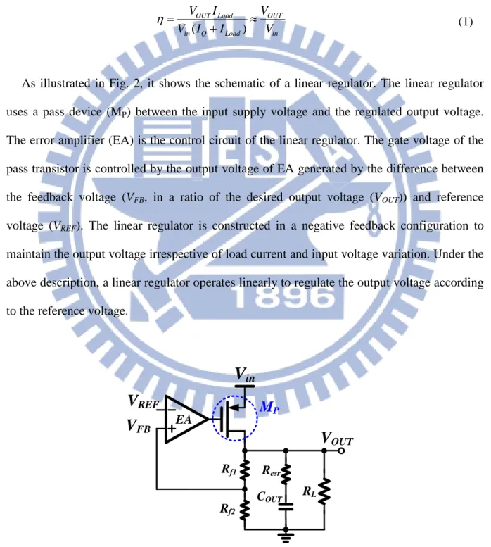
As illustrated in Fig. 2, it shows the schematic of a linear regulator. The linear regulator uses a pass device (MP) between the input supply voltage and the regulated output voltage.
The error amplifier (EA) is the control circuit of the linear regulator. The gate voltage of the pass transistor is controlled by the output voltage of EA generated by the difference between the feedback voltage (VFB, in a ratio of the desired output voltage (VOUT)) and reference
voltage (VREF). The linear regulator is constructed in a negative feedback configuration to
maintain the output voltage irrespective of load current and input voltage variation. Under the above description, a linear regulator operates linearly to regulate the output voltage according to the reference voltage.
V
REF Rf1 Rf2 COUT ResrV
OUT EA RLV
inM
PV
FB4
1.2.2 Switching Capacitor Regulator
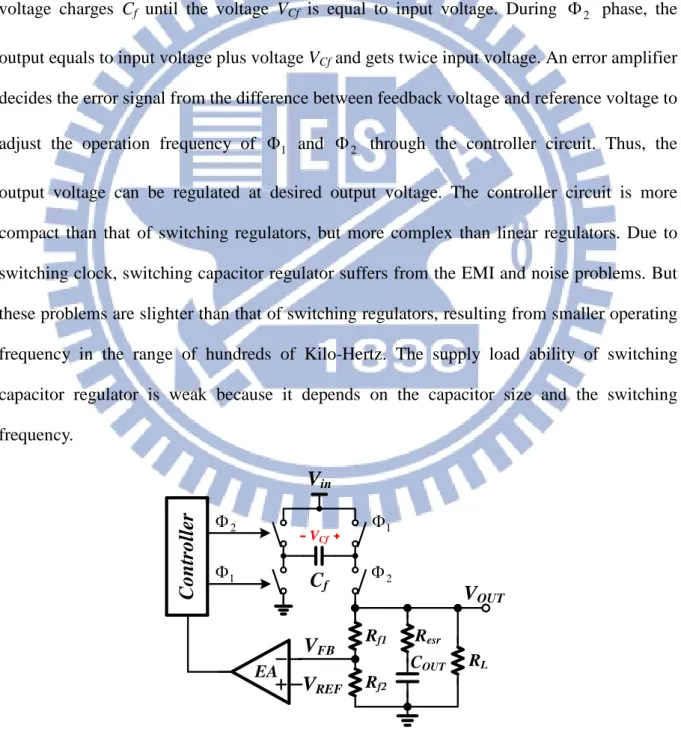
The switching capacitor regulator is usually used to obtain a DC voltage inverting or higher than the supply voltage in low load-current applications [5]-[8]. As shown in Fig. 3, this is a conventional switching capacitor regulator. There is no magnetic component, such as inductor, required comparing with the switching regulators. In the Φ phase period, the input 1 voltage charges Cf until the voltage VCf is equal to input voltage. During Φ phase, the 2
output equals to input voltage plus voltage VCf and gets twice input voltage. An error amplifier
decides the error signal from the difference between feedback voltage and reference voltage to adjust the operation frequency of Φ and 1 Φ through the controller circuit. Thus, the 2 output voltage can be regulated at desired output voltage. The controller circuit is more compact than that of switching regulators, but more complex than linear regulators. Due to switching clock, switching capacitor regulator suffers from the EMI and noise problems. But these problems are slighter than that of switching regulators, resulting from smaller operating frequency in the range of hundreds of Kilo-Hertz. The supply load ability of switching capacitor regulator is weak because it depends on the capacitor size and the switching frequency.
Controller
1 Φ 2 Φ Rf1 Rf2V
REF COUT RLV
OUTC
fV
in EA VCf 2 Φ 1 Φ ResrV
FB5
1.2.3 Switching Regulators
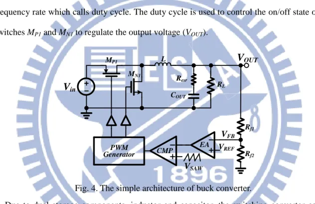
Switching regulators are widely used in power management IC because it has many excellent properties such as high power efficiency, high conversion ratio and programmable ability [9]-[18]. In Fig. 4, a simple architecture of voltage-mode buck converter, they are mixed-signal circuits which have both analog and digital blocks in the feedback loop. An analog signal, which is an error signal, is fed back to produce a digital signal at a certain frequency rate which calls duty cycle. The duty cycle is used to control the on/off state of the switches MP1 and MN1 to regulate the output voltage (VOUT).
V
in L COUTV
OUT MP1 VREF EA CMP PWM Generator VSAW Rf1 Rf2 VFB MN1 RL ResrFig. 4. The simple architecture of buck converter.
Due to dual storage components, inductor and capacitor, the switching converter can be operated in buck or boost operation. Generally speaking, the efficiency can be achieved above 90% under heavy load condition. Meanwhile, with higher switching frequency in the range from hundreds of Kilo-Hertz to several Mega-Hertz, the storage components can be designed smaller to save the cost. But the EMI and noise problems become critical. Depended on efficiency requirement, the control circuit is much larger than the other two regulators and the cost is the highest. However, the supply load ability is the largest in the range from about hundreds of milliamps to several amps.
6
functional-works, buck and boost converters, listed in Table I,
The first regulator is called as buck converter because of its property that steping down the input voltage with respect to output node. The conversion ratio M(D) of buck converter is written as M D( )=D. The second regulator is called as boost converter because of its property that steping up the input voltage with respect to output node. The conversion ratio
M(D) is written as ( ) 1 1 M D D = − .
There are many advantages of switching regulators compare with the linear regulators and switching capacitor regulators. Switching regulators have high current efficiency because they use power MOSFETs as switches and inductors, capacitors as energy storing elements. When the switched transistors operate in the cutoff region, it has no power dissipation. When the switched transistors operate in the triode region, it is nearly a short circuit with little voltage drop across it and has little power dissipation. Hence, most of the power dissipation is spent in the output node. A high power efficiency performance can be achieved numerically in the range 80% to 90%.
Table I. Two structures of switching regulators
Architecture Conversion Curve
Buck Boost + - Load Vin Vo Co L Control S1 S2 0.2 0.4 0.6 0.8 1.0 D Vi 0.2 0.4 0.6 0.8 1 0 + - Load Vin Vo Co L Control S2 S1 0.2 0.4 0.6 0.8 1.0 D Vi 1 2 3 4 5 0
7
Switching regulators also have disadvantages. There are larger complexity in circuit design of switching regulators than that of the linear regulators and also require discrete components such as inductors and capacitors. Furthermore, the transition response time and output noise are much larger than that of the linear regulators.
A comparison table between linear regulators, switching capacitor regulators and switching regulators are listed in Table II.
Table II: Comparisons of the different voltage regulators.
Linear
Regulators
Switching
Capacitor regulators
Switching
Regulators
Regulation Type buck buck/boost buck/boost/buck-boost
Efficiency Low Medium High
Complexity Low Medium High
Load ability Medium Low High
Chip Area Compact Moderate Large
EMI/Noise Low Medium High
Cost Low Medium High
1.3 Design Motivation
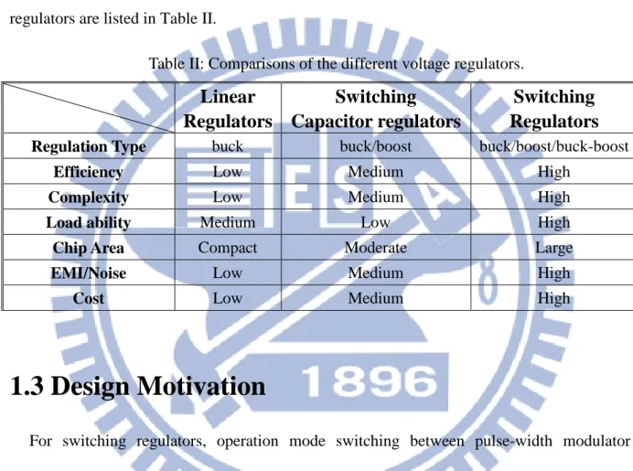
For switching regulators, operation mode switching between pulse-width modulator (PWM), pulse-frequency modulator (PFM) and pulse-skipping modulator are widely used to enhance the efficiency over the wide load range [19]-[24]. Besides, transient response is greatly improved by prior arts [25]-[30], such as Adaptive Pole-Zero Position (APZP) technique and dual-current pump. Moreover, in high-performance microprocessors applications, multiphase DC-DC converters are essential owing to its high current driving capability, small output voltage ripples and thermal management improvement [31]-[36].
Conventional PWM controller with a constant switching frequency is a suitable candidate for multiphase DC-DC converters. Nevertheless, the demand of complicated compensation
8
network, especially for the voltage-mode control, causes the vast increase of printed circuit board (PCB). Several methods make efforts on minimizing the area of the compensation elements [37]-[39]. Besides, to improve the load transient recovery time, the hysteresis-control DC-DC converters become an adequate solution to exhibit fast load transient response without the need of compensation components [42]. However, it suffers from synchronizing problem in multiphase applications. Although the delay-locked loop (DLL) controller can achieve synchronization between different phases with accurate duty cycle and large voltage conversion range [43], the power consumption and area occupation are substantially large.
Power stage 3 Power stage 2 RampN Power stage N Power stage 1 Current Sensing D1 Ramp3 Ramp1 Ramp2 Current Balance N
Logic Type III
Compensation DN Comp VREF Resr COUT RL RF1 RF2 VFB VOUT VIN L3 L2 L1 EA VC Comp Comp Comp D2D3 VCN VC3 VC2 VC1 VC3 VC1 VC2 VCN
Fig. 5. Conventional structure of the N-phase voltage-mode DC-DC buck converter. Conventional N-phase architecture as shown in Fig. 5 has high current driving capability as well as low output voltage ripple. N buck converter cells are implemented parallel in a voltage regulator module (VRM) to provide energy to the load simultaneously. In common with conventional voltage-mode DC-DC buck converter, each buck converter cell is controlled by one of the N independent controllers. In each controller, there contains a ramp generator, a comparator and a control logic circuit. Owing to the multiphase operation, N
9
interleaving ramp signals, Ramp1-RampN, are needed to compare with the error signals (VC1 -
VCN) carried out from the error amplifier for generating N interleaving duty cycles, D1 - DN,
for each phase. Obviously, the replicas of the controller derive large area and power dissipation.
1.4 Thesis Organization
In this thesis, the PRCB technique (Pseudo-Ramp Current Balance) is proposed to improve the performance and reduce circuit complexity in voltage-mode controlled multiphase DC-DC buck converter. The PRCB technique simply uses one controller to make multiphase operation and achieve high precision current balance comparing with the prior arts. The proposed PRCB technique are majorly divided into two parts, the pseudo-ramp technique and time-multiplexing current balance. Their description is given in the first part of Chapter 2. Besides the design concept, the system stability analysis is discussed and illustrated in the second part of Chapter 2. Detailed circuit implementations are presented in Chapter 3. Experimental results are shown in Chapter 4. Finally, a conclusion and future work are made in Chapter 5.
10
Chapter 2
P
ROPOSED
M
ULTIPHASE
S
TRUCTURE
AND THE
PRCB
O
PERATION
P
RINCIPLE
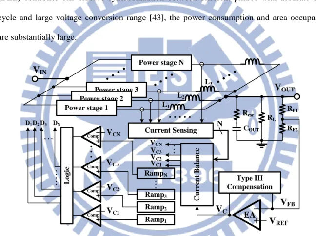
2.1 System Operation
Fig. 6 shows the proposed structure of N-phase DC-DC buck converter with the proposed PRCB technique. The N-phase power stages can simultaneously deliver energy to the output to improve the driving capability, and are controlled by a single controller to achieve an area-efficient operation. The power stage contains one P-type and one N-type power MOSFET. A dead-time control is used in the driver to prevent the short-through current problem. The voltage divider is composed of RF1 and RF2 to feed the information of output
voltage to the controller.
The main control scheme of the proposed multiphase converter is the voltage-mode operation [31], [34] and [40]-[42]. Thus, the Type III compensation is implemented to extend the system bandwidth and to obtain an adequate system phase margin. Particularly, there are only one saw-tooth signal and one comparator in the proposed design to control the N-phase power stages. In other words, the N-phase converter can be achieved with the elimination of the N-1 controllers in the proposed PRCB technique.
The pseudo-ramp operation and the current balance mechanism constitute the PRCB technique. The pseudo-ramp generator circuit can generate the fixed-frequency system clock
11
generated to ensure synchronization. Besides, the saw-tooth signal VSAW can be used to
determine the control signal VPWM through the comparison with the error signals VC, which is
carried out by the error amplifier (EA). Here, the proposed pseudo-ramp operation uses only one physical saw-tooth signal to obtain the multiple duty cycles (D1-DN) for multiphase
operation. MP MN Deadtime Driver Power stage N Power stage 3 Power stage 2 MP MN Deadtime Driver Power stage 1
V
IN L1 L2 L3 LN Current Sensing Circuit Current Balance Circuit Resr COUTV
OUT RL RF1 RF2 Phase Control LogicV
clk D1 DNV
PWMV
C Comp EAV
REF C2 C3 R3 R1 R2 C1V
FB VS1 IC1V
SAWV
MODE ICN Pseudo-Ramp Generator VSN Vck1 VckN VRPRCB
Fig. 6. Structure of the N-phase DC-DC buck converter with proposed PRCB technique. The phase control logic can realize the duty cycles, D1-DN, for the N-phase power stages
according to the multiphase clocks, Vck1-VckN, and the signal VPWM. Moreover, mode control
signal VMODE is used to determine the operation modes of the pseudo-ramp operation under
the different duty cycles. Specially, the auxiliary reference voltage VR is utilized to ensure the
12
On the other hand, the current balance mechanism is composed of the current sensing circuit and the current balance circuit. To ensure equal energy distribution in each of phases, the current sensing circuit can be used to sense the inductor current information during each phase. The sensed inductor current information, VS1-VSN, will be sent to the current balance
circuit, which can generate the signals, IC1-ICN, to adjust the duty cycles for each phase.
Therefore, the energy delivered by each of phases will be matched regardless of the mismatch problem derived between the N-phase power stages.
2.1.1 Pseudo-Ramp Operation
Fig. 7 shows the illustration of pseudo-ramp operation. Dual-phase topology is adopted to verify the proposed PRCB technique in this paper. The PRCB operation can be divided into two modes. It depends on the duty cycle smaller than 50 % or larger than 50 %, for Mode I or Mode II, respectively. Two clock periods, 2*Vclk, will constitute one complete switching cycle,
Ts, for two phases. That is, one pseudo-ramp is composed of two physical ramps in one
switching period.
In Mode I operation, the duty cycles D1 and D2 of the phase 1 and the phase 2, respectively,
are smaller than 50%. When the signal VMODE is high, as shown in the left-side of Fig. 7, the
duty cycle D1 of the phase 1 is determined by the intersection of the odd physical ramps,
which are part of the signal VSAW, and the error signal VC. Since the duty cycle is smaller than
50 %, the D1 can be determined within TS/2. That is in a physical ramp. On the other hand, the
duty cycle D2 of the phase 2 is decided by the even physical ramps of the signal VSAW. That
means the duty cycles D1 and D2 are carried out by the odd and even physical ramps,
respectively. In other words, the even physical ramps in the period of TS/2 to TS joins the
determination of the D2 and has no effect on the determination of the D1. In Mode I operation,
13
the dual-phase buck converter operation.
Once the duty cycle is larger than 50 %, the proposed PRCB technique will enter to the Mode II operation by setting the VMODE low. At the right-side of Fig. 7, it shows the
characteristic of the PRCB technique that can break through the limitation of 50 % duty cycle in dual-phase operation. Under Mode II control, alternatively, the D1 is determined by the
even physical ramps of the VSAW signal, and in consequence the D2 is decides by the odd
physical ramps. D1 is high (on state) during the odd physical ramps until the intersection of Vc
and the even physical ramps. When the view point is changed from the odd/even physical ramp into a continuous process, it is easy to find out the determination of D1 can be realised
with the black extended datted-line as show in Fig. 7. The idea of Pseudo-Ramp is carried out from here. Namely, two solid-line ramps constitute one datted-line pseudo-ramp, which has the switching period TS. The intersection of VC and pseudo-ramp can be extended from less
50% of TS to more than 50% of TS. Thus, the duty cycle D1 of amount larger than 50% can be
made. Similarly, the duty cycle D2 can be larger than 50%.
In the PRCB technique, two pseudo-ramps determine the dual-phase operation. Both D1
and D2 can be well-interleaved regardless the value of duty cycle. Most importantly, there is
only one physical ramp to determine the two interleaving duty cycles.
V
SAWV
clkD
1D
2V
C VMODE1
(Duty<50%) Pseudo Ramp 1 2 1 2 1 2 1 20
(Duty>50%)Mode I operation
Mode II operation
T
S14
However, the unstable scenario may happen when the duty cycle is exactly equal to 50% due to the discontinuous VSAW. In other words, the transition will induce a step increase in the
VC. To solve the transition between Mode I and Mode II, the deduction of the auxiliary
reference voltage VR from the EA’s output is activated for rapid response in the VC. As
illustrated in Fig. 8, the VR helps overcome the discontinuous duty cycle determination when
the duty cycle is close to 50 %. In addition, the duty blocking period (DBP) is also utilized in Mode II operation to avoid the duty cycle determination into the undistinguishable region. The DBP results in the phase shift of duty cycle in Mode II operation for stable operation because the proper duty cycle can be carried out. That is, the DBP helps define a hysteretic region to avoid the abnormal mode transitions triggered by switching noise.
V
SAWV
clkD
1D
2V
CV
MODE 1 2 1 2T
S 1 2 1 VR Duty Blocking1
0
Fig. 8. The timing diagrams when the DBP is utilized.
Moreover, the mode transition operation contributes the enhancement of transient response. In case of a sudden load current increase, the voltage drop induces a rapid variation at the VC
by the EA. Large increase in the VC will lead to the mode transition from Mode I to Mode II if
the VC exceeds the amplitude of physical ramps. Thus, a resultant increase in the duty cycle
will provide extra energy to compensate the insufficient driving capability so as to enhance the load transient response. The similar operation would occur when a large decrease of load happens.
15
2.1.2 Time-Multiplexing Current Balance Mechanism
Ideally, if each of the individual phases derives the identical duty cycles, D1=D2=…DN, the
inductor current in each individual phase will be theoretically equal in the multiphase operation. However, the inevitable mismatches existing among the N power stages and PCB boards will cause enormously unbalanced current distribution. Thus, the current balance mechanism is demanded to compensate the unbalanced scenario by automatically adjusting the duty cycles by d tˆ ( )i (where i=1, 2, 3… and N). Thus, the adjusted duty cycle of each
phase becomes ( ) ˆ( )
i i i
d t =D+d t (where i=1, 2, 3… and N) to achieve current balance. Fig. 9
shows the implemented current balance mechanism in the proposed PRCB technique.
If one of the two phases has large driving current, the duty cycle, which causes large driving current, needs to decrease. Contrarily, the other duty cycle is required to increase. Owing to the voltage-mode operation in the monolithic control scheme, the duty cycles are determined through the comparison of the VSAW and the VC. [40]-[42] However, in the PRCB
technique, it is improbable to adjust the VC for current balance since the change in the VC will
lead both duty cycles to increase or decrease simultaneously. Alternatively, the modulation in the VSAW is used to achieve the dual-phase current balance in the PRCB technique [44].
The time-multiplexing current balance mechanism is activated in the PRCB technique according to the distinct operation modes. In the Mode I, the ramp adjustments for the d1(t)
and d2(t) act on the odd and even ramps, respectively. If the inductor current IL1 in phase 1 is
larger than the IL2 in phase 2, the increase of the odd ramp slopes will lead the decrease of the
d1(t) to reduce the current driving capability in phase 1. Besides, the increase of d2(t) in phase
2 will enhance its current driving capability by decreasing the even ramp slopes. Similarly, in case of large IL2 and small IL1, the current balance can also be ensured in the Mode I.
16
adjustment will work in an alternative way to fit the pseudo-ramp operation. The odd ramp slopes are decreased while the even ramp slopes are increased to reduce the d1(t) and to
enlarge the d2(t) when the IL1 is larger than the IL2. The similar operation is achieved when the
IL1 is smaller than the IL2 in the Mode II. Therefore, the current balance mechanism can be
realized by adjusting the ramp signals both in the Mode I and the Mode II. In other words, current balance is achieved under the whole duty cycle range.
Mode II operation VSAW VC V SAW VC D1 D2 VSAW VC VSAW VC VSAW VC D1 D2 VSAW VC Mode I operation Duty > 50% Duty < 50% VMODE 1 0 IL1>IL2 IL1>IL2 IL1<IL2 IL1<IL2 ˆ 1+ 1 D d (t) ˆ 2+ 2 D d (t) ˆ 1+ 1 D d (t) ˆ 2+ 2 D d (t) ˆ 1+ 1 D d (t) ˆ 2+ 2 D d (t) ˆ 1+ 1 D d (t) ˆ 2+ 2 D d (t)
Fig. 9. Current balance mechanism implemented with pseudo-ramp operation in the proposed dual-phase DC-DC buck converter.
2.2 Stability Analysis of the Multiphase Converter
with the PRCB Technique
To ensure the system stability, not only the proposed PRCB technique but also the TM current balance technique should be modeled accurately. In this work, a dual-phase converter is modeled to verify the system stability.
17
2.2.1 The Model of the Pseudo-Ramp Technique
Equivalent model of the two-phase converter with the pseudo ramp technique is shown in Fig. 10 [45]. In frequency domain, the duty cycle can be expressed as (2).
ˆ
( ) ( ) where 1 or 2
i i i
d s =D +d s i= (2)
ˆ ( )i
d s is the duty cycle variation caused by the TM current balance technique. Di is the duty
cycle without the current balance function. Theoretically, D1 and D2 are equal to the average
duty cycle as shown in (3).
1( ) 2( )where 1 or 2
2
d s d s
D= + i= (3)
The feedback voltage VFB(s) is acquired by the voltage divider with the gain of H(s). The
difference of the Vref and the VFB(s) is amplified by the error amplifier to produce the error
signal VC(s). The modulator compares the VC(s) with the ramp signal to generate the duty
cycles, d1(s) and d2(s), for phase 1 and phase 2, respectively.
VIN(s) VC(s) VOUT(s) H(s) Gc(s) VFB(s) Vref FM d2(s) Gvd(s) FM d1(s) Gvd(s) Gvg(s) Zout(s) iload(s)
Converter power stage Ve(s)
Fig. 10. Equivalent model of the two-phase converter with the pseudo-ramp technique. The open-loop output impedance Zout(s), the line-to-output transfer function Gvg(s), and the
18 2 ( ) 1 out L sL Z s L s s LC R = + + (4) 2 1 ( ) 1 vg L G s D L s s LC R = ⋅ + + (5) 2 1 ( ) 1 OUT vd L V G s L D s s LC R = ⋅ + + (6)
L, C, and RL are the filter inductor, capacitor, and equivalent load resistance, respectively.
In the pseudo-ramp control, all phases share the same ramp. Similar to the conventional architecture of multiple controllers, it is convenient to model separately the modulator of each phase. The effective magnitude of pseudo-ramp is twice of the physical ramp amplitude VM.
Thus, the modulator gain, FM, can be written as (7). 1 2 M M F V = (7)
Considering the stability problem, Type III compensation is adopted to compensate the complex poles caused by the L, C. Fortunately, only one set of Type III compensator is required since the PRCB technique has single controller. Besides, the design of the Type III compensation is simply the same as single phase operation.
2.2.2 TM Current Balance Model
TM current balance can be achieved by comparing the adjusted ramp with the error signal
VC(s). To fit the characteristic of the adjusted ramp, the model of the pulse-width modulator
needs to be modified as shown in Fig. 11(a). The difference of the current sensing signals, VS1
19
the current-balance control signals IC1(s) and IC2(s). The IC1(s) and IC2(s) are injected to the
ramp signal capacitor Cramp to adjust the amplitude by ΔVMi (i=1 or 2) as depicted in Fig. 11(b).
The equivalent variation in the duty cycle is equal to d sˆ ( )1 (or d sˆ ( )2 ), which causes the duty
varies from D1 (or D2) to D1±d sˆ ( )1 (or D2±d sˆ ( )2 ). Thus, the modified duty cycles d1(s) and
d2(s) can achieve good current balance.
VC(s) FMV d1(s) ord2(s) IC1(s) or IC2(s) FMC(s)
F
M Vce1(s) or Vce2(s) or ˆ VC1(s) VˆC2(s) VC ΔVM1 or ΔVM2 VM D1 or D2 d1(s) or d2(s) or Vce1 or Vce2 Adjusted ramp Original ramp ˆ 1 d (s)or d (s)ˆ2 ˆ C1 V (s) ˆ C2 V (s) (a) (b)Fig. 11. (a) Equivalent model of the pulse-width modulator with the current balance. (b) The relationship between the duty cycle and the adjusted ramp.
Without the current balance function, the duty cycle is obtained by comparing the error signal Vc(s) with the original ramp. For the two phases, the original duty cycles are D1 and D2
as shown in (8). ( ) ( ) ( 1 or 2) 2 C i M V s D s i V = = (8)
Here, the ΔVMi, which can be either a positive or a negative value, contributed by the
current balance circuit compensates current unbalance circumstance to adjust the ramp amplitude VM+ΔVMi (i=1 or 2). Comparing the adjusted ramp with the Vc(s), the duty cycle
di(s) (i=1 or 2) with the current balance can be expressed in (9).
( ) ( ) ( 1 or 2) 2( ) C i M Mi V s d s i V V = = + ∆ (9)
20
Since the ΔVMi is produced by injecting the current-balance control signal IC1(s) (or IC2(s))
into the ramp capacitor Cramp during the period of Ts/2 for each phase, the ΔVMi can be derived
as (10). 1 ( ) (where 1 or 2) 2 s Mi Ci ramp T V I s i C ∆ = ⋅ ⋅ = (10)
According to (8), (9) and (10), the duty cycle variation is given by (11).
( ) ˆ ( ) ( ) 2 ( ) ( ) ( 1 or 2) 2 C Mi i i i M M Mi Mi Ci s M M ramp V s V d s d s D V V V V DI s T D i V V C ∆ = − = − ⋅ + ∆ ∆ ≈ − = − = (11)
As a result, the adjusted-current-to-duty transfer function can be derived as shown in (12).
ˆ ( ) ( ) 2 i s Ci M ramp d s DT I s ≈ V C (12)
The model of the PRCB technique with the current balance is complicated since the duty cycle is determined by many factors. To simplify the model, the duty cycle variation d sˆ ( )1 (or
2 ˆ ( )
d s ) is transferred to the error signal variation Vˆ ( )C1 s (or Vˆ ( )C2 s ). Thus, the pseudo-ramp
modulator can be divided in to two blocks, the voltage modulator FMV and the current
modulator FMC(s). With the TM current balance technique, the error signal variationVˆ ( )C1 s (or 2
ˆ ( )C
V s ) is subtracted from the original error signal VC(s) to generate the effective error signal
Vce1(s) (or Vce2(s)). Comparing the Vce1(s) (or Vce2(s)) with the original ramp signal is able to
obtain the duty cycle d1(s) (or d2(s)), which is equal to the comparison of the error signal VC(s)
and the adjusted ramp signal. Here, the voltage modulator FMV in (13) remains the same as
(7). 1 2 MV M M F F V = = (13)
21
Besides, the current modulator 𝐹𝑀𝐶(𝑠) is derived as (14). Here shows a fact that the current balance effect is in relation with the magnitude of the average duty cycle. As D becames larger, the effect of 𝐹𝑀𝐶(𝑠) is greater because of capacitor integration.
ˆ ˆ ( ) ˆ ( ) ( ) ( ) ˆ ( ) ( ) ( ) 2 1 or 2 2 Ci Ci i MC Ci i Ci s s M M ramp ramp V s V s d s F s I s d s I s DT DT V i V C C = = ⋅ = ⋅ = ( = ) (14)
2.2.3 System Stability Analysis
In spite of the disturbance of input voltage and load current, eventually, the equivalent model of the PRCB technique with the TM current balance is depicted in Fig. 12. Except for the voltage loop, the TM current balance loop as well as the cross coupling loop are also included. The voltage loop is defined as (15).
( ) ( ) ( ) ( )
v c MV vd
T s =G s F G s H s (15)
In the current balance loop, the two-phase inductor currents are sensed by the Ri and hold
by the sample-and-hold circuits to generate the signals, VSH1(s) and VSH2(s). The sensing and
sampling effect will introduce a pair of complex RHP zeros at half of the switching frequency [28]. The transform function can be expressed as (16).
2 n 2 2 ( ) 1 where and e n n n n s s s H s Q Q T π ω ω ω π ≈ + + = − = (16)
22 Gid(s) Gid(s) Gid(s) Ri He(s) Ri He(s) VSH1(s) VSH2(s) AOTA(s) GV-I(s) IC1(s) FMC(s) FMV d1(s) IL1(s) IL2(s) -1 GV-I(s) IC2(s) FMC(s) FMV d2(s) Gvd(s) Gvd(s) VOUT(s) H(s) Gc(s) VFB(s) Vc(s) Vce2(s) Vce1(s) cc id G (s) cc id G (s) VIC1(s) VIC2(s) ˆ C2 V (s) ˆ C1 V (s)
Fig. 12. Equivalent model of dual-phase buck converter with the PRCB technique and the TM current balance.
The difference of the VSH1(s) and the VSH2(s) will be amplified by operational
transconductance amplifier AOTA(s) to obtain the current balance control voltages, VIC1(s) and
VIC2(s). The V-to-I converter GV-I(s) converts the VIC1(s) and the VIC2(s) to the current balance
control currents, the IC1(s) and the IC2(s), respectively, which can adjust the d1(s) and the d2(s),
respectively. The duty-to-current transform function is derived in (17) for each phase.
( ) [ ] e 2 1 0 0 0 0 e e 1 e 1 ( ) where ( ) and L sr OUT id DCR L L DCR sr DCR sr L sr sC R R V G s D s LCR s Q R R Q L C R R R R R R R R ω ω + + = + + + = + + + = + (17) The characteristic of current loop is the crucial of the TM current balance technique. Ideally, a stable current loop will not have influence on the output voltage. Furthermore, the
23
operation of current balance loop is independent of load current but relies on the difference of the dual-phase inductor currents. Therefore, the output can be regarded as shorted ground. The duty-to-current transform function is modified as (18).
0 1 ( ) OUT OUT id V DCR V G s D sL R = = ⋅ + (18)
Since the TM current balance scheme is based on the average current balance control, the small signals in two phases are the same in magnitude and opposite in phase [34]. That is,
1 2
ˆ ˆ
SH SH
V = −V , VˆIC1= −VˆIC2, IˆC1= −IˆC2 , dˆ1= −dˆ2, and IˆL1= −IˆL2 . Consequently, the two loops in dual-phase operation become symmetric and thus are added as shown in Fig. 13. Thus, the TM current balance loop gain is derived as (19).
( ) 2 ( ) ( ) ( ) ( ) ( ) cb OTA V I MC MV id shorted i e T s = A s G − s F s F G s R H s (19) ˆ ˆ I or I L1 L2
R
iH
e(s)
2A
OTA(s)
G
V-I(s)
F
MC(s)
F
MVT
cb(s)
OUT=0 id VG (s)
ˆ ˆ V or V SH1 SH2 ˆ (s)or ˆ (s) d1 d2 ˆ ˆ IC1 or IC2 ˆ ˆ VIC1 or VIC2 ˆ ˆ C1 or C2 V VFig. 13. Small signal model of the TM current balance loop.
Ideally, the inductor current is controlled by its own current balance control signal. However, the inductor current in one phase will be affected by the change in duty cycle of another phase inevitably [47]. Therefore, the cross coupling effect has to be taken into consideration in system stability analysis. The cross coupling duty-to-current transform function can be derived as (20).
24 [ ] e 2 1 e e 1 e (1 ) 1 ( ) ( ) 2 where ( 2 ) and cc OUT L sr id DCR cc cc DCR L cc cc L DCR sr DCR sr L sr V R sCR G s D sL R s LCR s Q R R Q L C R R R R R R R R ω ω + = − + + + + = + + + = + (20) And the cross coupling loop can be defined as (21).
( ) ( ) ( ) ( ) cc( ) ( )
cc OTA V I MC MV id i e
T s = −A s G − s F s F G s R H s (21)
In the proposed structure, a compensation capacitor is located at the output of the operational transconductance amplifier. The added compensation pole not only ensures the stability of current balance loop Tcb(s) but also compensates the cross coupling loop Tcc(s).
The bode plot of loops Tv(s), Tcb(s) and Tcc(s) is shown in Fig. 14. The DC gain and the phase
margin of the Tv(s) are 91.9 dB and 51∘ while the DC gains and the phase margins of the Tcb(s)
and the Tcc(s) are (24.7 dB, 52∘) and (12.2dB, 86∘), respectively. With the stabilized loops, the
system stability is assured.
Bode Diagram
Tv(s) Tv(s) Tcb(s) Tcb(s) Tcc(s) Tcc(s)Magnitude
(dB
)
Phase
(deg
)
Frequency (Hz)
25
Moreover, the voltage loop dominates the operation of the whole multi-phase system. In other words, the voltage loop gain is designed to be higher the current balance loop gain. Bandwidths of both loops are desired as large as possible in general design to accelerate the transient response. However, the enlarged bandwidth of the current balance loop would slow down load transient response due to the lack of rapidly increasing inductor current. For instance, in case of light-to-heavy load variation, one of the phases must suddenly prolong the on-time to cope with the lack of energy. Consequently, it causes current unbalance inevitably. Simultaneous, the current balance loop will start to pull down the unbalance inductor current. Owing to the enlarged bandwidth, the suppression of energy provided to output will be reduced by the fast current balance loop. More switching cycles are needed to regulate output voltage. As a result, loop gain and bandwidth of the two loops have to be carefully designed to meet the specification.
26
Chapter 3
C
IRCUIT
I
MPLEMENTATION
3.1 Current Sensing Circuit
For current balance, the inductor current information of each phase needs to be detected to modulate the individual duty cycles. The simplest way to achieve current sensing is to implement an auxiliary resistor in series with the power switch. It induces large power dissipation so as to deteriorate the power conversion efficiency [47]-[48]. Therefore, Fig. 15 shows the utilized current sensing circuit with the replica current flowing through the sensing switch [10]. The power transistor MP conducts the inductor current during its turn-on period.
The common-gate amplifier, which is composed of M2-M5, can ensure the near
source-to-drain voltages between the MP and the sensing MOSFET MS1. Thus, the sensing
current Isen as the replica of the inductor current depends on the aspect ratio between the MP
and the MS1.
The Isen flows through the M6 and the sensing resistor RS to carry out the current sensing
signal VS. Besides, to enhance the current sensing accuracy, the M7, which has the same aspect
ratio as the current mirror structure, the M2 and the M3, is added to provide a compensative
current, IB. Moreover, the sensing speed of the proposed current sensing circuit can be
improved since the common-gate gain stage derives large operation bandwidth since no compensation component is demanded in this structure [49].
27 IB
V
S 1 RS M2 M3 M1 M4 M 5 M6 M7M
S1M
PD
1L
1 RP LX1 IB IB IB IsenFig. 15. The current sensing circuit.
3.2 Current Balance Circuit
Current balance mechanism in the multiphase structure can ensure equivalent current driven capability of each phase. As shown in Fig. 16, the proposed current balance circuit, which contains the current matching unit and the voltage averaging element, is used to adjust the saw-tooth signal generated by the pseudo-ramp generator circuit, as well as the duty cycles for matched inductor current levels. The sensing signals, VS1 and VS2, derived from the
current sensing circuits will be sent into the current matching unit. The sample-and-hold (SH) circuit is activated to obtain the voltages, VSH1 and VSH2, for representing the average inductor
current level of each phase.
To get an accurate current balance, the voltage averaging element is used to derive the average value Vavg for the phase current distribution. That is, a high-gain operational
transconductance amplifier (OTA) is realized to reflect the current difference between the average value and each of the phases. The voltage difference will be amplified to generate the current balance control signals, VIC1 and VIC2. VIC1 and VIC2 are converted to the difference
injection currents IC1 and IC2, respectively, which are injected into the pseudo-ramp generator
28
accuracy, the capacitor Cc is used to stabilize the current-loop operation. As a result, both of
the on-chip and off-chip mismatch issues will be well compensated through the current balance control scheme. Only one controller is utilized to achieve high accuracy and area and conversion efficiency in the proposed PRCB technique.
R1
Current matching unit
OP R2 OP
V
avg R3 2R R 2R MS1 MS2 MS3 MS5 MS6 MS4I
C2I
C1V
S1V
S2V
SH1V
SH2 Cc OTA CS1 CH1 Sample-and-hold R1 M2 M3 V-I converterCurrent matching unit
V
SH1V
avgVoltage averaging element
V
IC1Fig. 16. Current balance circuit.
3.3 Pseudo-Ramp Generator
Fig. 17(a) shows the schematic of the pseudo-ramp generator. A fixed frequency signal Vclk
is derived through the fixed frequency generator composed of M1-M7 and the capacitor C1.
The reference voltages VH and VL are derived from the bandgap circuit to determine the
frequency of Vclk with the bias current IB. Thus, the Vclk can be used to control the switches,
M9 and M10, to generate the saw-tooth signal VSAW through the charging and discharging of
Cramp for achieving the PRCB technique.
29
equal. That is, each of the ramps of VSAW is identical so as to realize the same duty cycle for
the dual-phase operation. However, once the current unbalance operation occurs, the current balance circuit will detect the current difference between the two phases to modulate the IC1
and the IC2 and thus to modify the VSAW. By alternatively injecting the IC1 and the IC2, the odd
and even ramps in the VSAW will be changed to adaptively adjust the duty cycles as well as the
dual-phase inductor currents. The compensated current injection is also controlled by the signal VMODE to properly generate the pseudo-ramp signal for different operation modes.
The timing diagram of the pseudo-ramp generator circuit is depicted in Fig. 17(b). Moreover, a frequency divider is implemented to carry out the two phase clocks, Vck1 and Vck2,
for the dual-phase operation. The Vck1 and the Vck2, indicate the beginning of the switching
cycle of phase 1 and phase 2, respectively. Consequently, the phase control logic can produce individual duty cycle for each power stage.
Fixed frequency generator IB Comp Comp VH VL R Q Q S
V
clk M1 M2 M3 M8 M4 M5 M6 M7 M9 M10I
C2I
C1V
SAW C1 CrampV
MODEV
SEL D Q Q 0 1 M UXV
ck1V
ck2V
SEL 0 1 M UX (a)30
V
clkV
ck1V
ck2V
SELV
MODEV
SAW0
1
(b)Fig. 17. The pseudo-ramp generator. (a) Schematic (b) Time diagrams
3.4 Phase Control Logic
Fig. 18 shows the implementation and the operation of phase control logic. Fig.18(a) shows the schematic of phase control logic, which is composed of the duty generator unit and the mode transition unit. The signals Vclk, Vck1, and Vck2 are generated from the pseudo-ramp
generator. The Vck1 and the Vck2 are used to indicate phase 1 and phase 2, respectively, because
there is only one saw-tooth signal to determine the duty cycle. The VPWM is the resultant duty
determination derived from the comparison of the VSAW and the VC in the proposed
pseudo-ramp operation. The Vck1 and the Vck2 can activate the D1 and the D2, respectively. In
the meanwhile, the rising edge of the VPWM is used to reset the duty cycles and thus wait for
the next triggering. The operation time diagram is depicted in Fig. 18(b).
The mode transition unit is used to decide the operation mode according to the duty cycle. With a continuously increasing duty cycle in the Mode I, the D1 or the D2 would overlap with
the Vck2 or the Vck1, respectively. Thus, the VM1 or the VM4 will indicate the exceeding duty
cycle of 50 %. The overlapping of the D1 and the Vck2 (or that of the D2 and the Vck1)
represents that the duty cycle in the Mode I has taken over the full period of one physical ramp in the VSAW. Once it occurs, the operation mode will transit from the Mode I to the Mode
31
On the other hand, if the duty cycle is continuously decreasing in the Mode II, it would enter the boundary region of duty determination. When both the D1 and the D2 do not cover
the entire period of the Vck2 and the Vck1, respectively, the duty cycle is smaller than 50 %. To
ensure the proper pseudo-ramp operation, the operation mode will change from the Mode II to the Mode I. Detailed flow chart of the mode transition operation is shown in Fig. 18(c).
D Q Q
V
clk D Q Q CLRV
ck2D
1V
SET D Q Q CLR D Q Q CLRV
ck1D
2 D Q Q CLR R Q Q SV
MODE VM1 VM2 VM3 VM4 R Q Q S Duty generator 1D
1D
2Duty generator 2
V
MODEV
PWMV
ck2V
ck1V
SETMode
transition unit
(a)32
V
ck1V
ck2V
MODE1
V
PWMD
1D
21
0
V
SAWV
CDuty cycle Duty cycle
V
SET (b)Start
Mode I or Mode II
I
L1Odd-Ramps
I
L2Even-Ramps
I
L1Even-Ramps
I
L2Odd-Ramps
V
M1=1 V
M4=1
V
M2=1 V
M3=1
Switch to Mode II
(V
MODE=0)
Switch to Mode I
(V
MODE=1)
YES
YES
NO
NO
Mode I
(V
MODE=1)
Mode II
(V
MODE=0)
Mode transition unit
(c)
Fig. 18. (a) Implementation of the phase control logic. (b) Time diagram of the phase control logic. (c) Flow chart of the mode transient operation.
33
Chapter 4
E
XPERIMENTAL
R
ESULTS
4.1 Chip Micrograph and Design Specification
The proposed multiphase DC-DC buck converter with the PRCB technique was fabricated in 0.25 μm CMOS process. Dual power stages are embedded in the test chip for verification. The utilization of off-chip inductors and capacitors are 4.7 μH and 47 μF, respectively. The chip micrograph is shown in Fig. 19 with an active silicon area of 3.91 mm2. Power stages of phase 1 and phase 2 are placed closed to bond pads. The single controller is implemented in the middle of the chip so as to minimize the mismatches issues for both power stages. The key design specifications are listed in Table III.
2300 μm
1700
μ
m
Power
stage
Phase 1
Controller
Power
stage
Phase 2
34
TABLE III: Design specification of the PRCB multiphase voltage buck converter Technology 0.25m μm CMOS process
Inductor / DCR 4.7 μH/ 100 mΩ (nominal) Capacitor /ESR 47 μF/ 50 mΩ (nominal) Switching Frequency 600 kHz
Input Voltage (VIN) 3.3 V – 5 V
Output Voltage range (VOUT) 0.8 V – 3 V (VIN = 3.3 V)
Load Current range (ILoad) 0 mA – 2000mA
Current balance improvement (%) Min. 83% Power conversion efficiency Max. 88 % Chip size 3.91 mm2
4.2 Steady-State Operation Results
Fig. 20 shows the measured steady-state operation. With the input voltage VIN of 3.3 V, the
nominal output voltage VOUT is 2 V. The switching frequency is 600 kHz. The mismatch from
the size of power MOSFETs and the DCR of inductors between each phase results in current unbalance. The proposed pseudo-ramp operation can generate the proper duty cycles for the dual-phase operation with a 12 mV output voltage ripple. Besides, the current balance mechanism achieves the current matching. Fig. 21 shows the measured steady-state operation with the load current of 500 mA. The pseudo ramp can decide the correct duty cycles so as to guarantee the output voltage regulation. The current difference between the dual phases is reduced to 1.9 mA, which can verify the operation of the proposed current balance mechanism in the PRCB technique.
35
V
OUTI
L1I
L212mV
Dual phase current matching
Steady-state operation
I
load=0mA
Fig. 20. Measured steady-state operation result with the VIN of 3.3 V.
Steady-state operation
V
OUTV
MODEI
L1I
L2w/i current balance ΔI
L=|I
L1-I
L2|=1.9mA
I
Load=500mA
Fig. 21. Measured steady-state operation result with ILoad of 500mA.
4.3 Load Transient Response
Fig. 22 shows the measured load transient response with the load changes between 0 mA and 550 mA. The voltage drop and overshoot are about 70 mV and 40 mV, respectively. The current balance mechanism is achieved in the period of load transient response as well.
36
Load transient response
V
OUTV
MODEI
L1&
I
L2I
Load
=0mA between 550mA
Duty=40%
70mV
40mV
Fig. 22. Measured load transient response with the current balance mechanism.
The mode transition operation is shown in Fig. 23 The operation mode would be changed from the Mode I to the Mode II during the load transient period so as to enlarge the duty cycles to derive extra energy. In Fig. 23(a), the load current steps from 0 mA to 550mA and the recovery time is long since the mode transition function is closed for comparison. The second experiment result as shown in Fig. 23(b), which shows a shorter recovery time, is taken to examine the load transient improvement with the mode transition function opened. Thus, as shown in the experimental results, the mode transition operation can help minimize the voltage drop and shorten the transient response time to enhance the load transient operation. The operation mode may be switched back to the Mode I once the load transient period is terminated. However, the DBP mechanism helps define a hysteretic region to avoid the abnormal mode transitions triggered by switching noise. Therefore, the converter will keep operating in the Mode II until the surplus energy is detected at the output.
37
Load transient response
V
OUTV
MODEI
L1&
I
L2I
Load=500mA
Duty=40% (a)Mode switch improves transient response
Load transient response
V
OUTV
MODEI
L1&
I
L2I
Load=500mA
Duty=40% 50 μs (b)Fig. 23. Experimental results of load transient response (a) without mode switching strategy and (b) with the mode switching strategy.
4.4 Line Transient Response
As described in the foregoing sections, Mode I and Mode II are used for duty cycle smaller and larger than 50%, respectively. To show the relation between the variations of duty cycle, caused by the input voltage, with the mode transition operation, the line transient response of