國立交通大學
電子工程學系電子研究所
碩士論文
金屬閘高介電n型金氧半場效電晶體及
鰭式電晶體閘極電子穿隧電流的精確模擬
Accurate Modeling of
Gate Electron Tunneling Current in
Metal-Gate/High-K nMOSFET and nFinFET
研究生:張洛豪 Lou-Hao Chang
指導教授:陳明哲 Prof. Ming-Jer Chen
金屬閘高介電n型金氧半場效電晶體及
鰭式電晶體閘極電子穿隧電流的精確模擬
Accurate Modeling of
Gate Electron Tunneling Current in
Metal-Gate/High-K nMOSFET and nFinFET
研究生:張洛豪 Lou-Hao Chang
指導教授:陳明哲 Prof. Ming-Jer Chen
國立交通大學
電子工程學系電子研究所
碩士論文
A Thesis
Submitted to Department of Electronics Engineering &
Institute of Electronics
College of Electrical and Computer Engineering
National Chiao Tung University
in Partial Fulfillment of the Requirements
for the Degree of
Master of Science
in
Electronics Engineering
August 2011
Hsinchu, Taiwan, Republic of China
中華民國 一00 年 八 月
金屬閘高介電n型金氧半場效電晶體及
鰭式電晶體閘極電子穿隧電流的精確模擬
研究生:張洛豪 指導教授:陳明哲 國立交通大學 電子工程學系電子研究所摘要
高介電質絕緣層可以抑制閘極漏電流而鰭式金氧半電晶體結構可以改善短 通道效應的影響。藉由WKB近似理論建立的閘極穿隧電流已經被發表了。在本 篇論文中,將會說明電子通過雙閘極元件中高介電質絕緣層的穿隧模型,而且將 此模型應用到n型鰭式金氧半電晶體中。由於元件從單個閘極變成多閘極的結構, 電子在各個能帶中擁有的能量公式需要被修正。藉由改變曲線擬合因數,修正後 應用於雙層閘集結構的模型對於不同基底厚度依然成立。將滿足修正變數線性方 程式中的基底厚度改變,只要知道基底厚度,修正變數就能夠被確定。 除了閘極電容電壓及閘極電流電壓的資料曲線擬合外,量測元件中的相關材 料係數可以由進一步的對閘極電流取對數的曲線擬合得到更為正確的結果。由於 高介電值層和介面層的介電係數差太大,平緩的過度漸層介於此兩層中加入,能 改善對於在高電場中電流的曲線擬合。 由這幾個修正,測量的資料和模擬數據電流可以吻合。這可以更加了解電子 在鰭式金氧半電晶體中的穿隧機制。Accurate Modeling of
Gate Electron Tunneling Current in
Metal-Gate/High-K nMOSFET and nFinFET
Student: Lou-Hao Chang Advisor: Prof. Ming-Jer Chen
Department of Electronics Engineering and Institute of Electronics
National Chiao Tung University
Abstract
High-K stacks cansuppress the gate leakage current while a FinFET structure has
benefits of improving the short channel effects. Gate tunneling current model has
been established based on WKB approximation. In this thesis, an electron tunneling
model through high-K stacks will be constructed for double-gate devices, especially
n-type FinFET. The electron subband energy should be modified for the change of the
structure from single gate to multiple gates. This model established for double gate
structure is also valid for different body thicknesses through different fitting factors
used. A linear relation is obtained between body thickness and the subband fitting
factor. Once the body thickness is known, the fitting factors can be determined
accordingly.
Material parameters of the experimental devices can be accurately determined by a
new fitting of dln(Ig)/dVg-Vg in combination with the conventional Cg-Vg and Ig-Vg
fittings. A gradual transition layer between high-K layer and interfacial layer can
improve the fitting quality at high gate voltages owing to the large difference of
permittivity between high-K dielectric and interfacial layer. With these modifications
The new model can also lead us to a better understanding of the gate tunneling
Acknowledgement
碩士班兩年時間,在實驗室每周開會時間,陳明哲教授對於學術界的熱情以 及學問的淵博,讓我在報告時候,研究瓶頸的時刻,由教授提供的意見及方向, 能夠繼續一步步的完成論文的研究,由衷感謝老師這段時間的指導。也謝謝百忙 之中抽空參加我口試的口試委員們,對於我的研究上提供意見。 在實驗室中,博士班李建志、許智育、李韋漢與張立鳴學長們對於我課業上、 生活上各種問題提供了解決方法,而許智育學長在這段期間,有他的指導與幫助, 使我的研究能夠順利進行。 感謝實驗室的研究夥伴們,與光心君、彭霖祥一起互相鼓勵與討論,學弟妹 們在課業上以及準備口試上也給予我極大的幫助,跟大家一起度過在實驗室的時 間,是這兩年讓我很開心的事。 還有感謝在就學期間,全力支持以及鼓勵我的家人,有了他們的一席鼓勵的 話,讓我更有動力去完成及克服遇到的困難。Contents
Abstrate (Chinese)
... I
Abstrate (English)
... II
Acknowledgement
... IV
Figure Captions
... VII
Chapter 1 Introduction
... 1
1.1 Background
... 1
1.2 Arrangement of This Thesis
... 2
Chapter 2 Physical Model for Planar FET
... 4
2.1 Tunneling Current Model for Oxide Dielectric
... 4
A.
Inversion Layer Charge (N
i,j)
... 5
B.
Electron Impact Frequency (f
j)
... 5
C.
WKB Transmission Probability (T
WKB)
... 6
D.
Reflection Correction Factor (T
R)
... 7
2.2 Modified Tunneling Current Model for High-K Gate Stacks
.... 8
A.
Modified WKB Transmission Probability for High-K Stacks
(T
WKB)
... 8
B.
Modified Reflection Correction Factor for High-K Stacks
(T
R)
... 9
2.3 Subband Energy Calculation
... 10
Chapter 3 Physical Model for FinFET
... 13
3.1 Depletion Charge Density Calculation
... 13
3.2 Subband Energy Calculation for FinFET
... 14
Chapter 4 Metal-Gate/High-K FinFET: Experiment and Fitting
... 18
Chapter 5 Conclusion
... 21
References
... 23
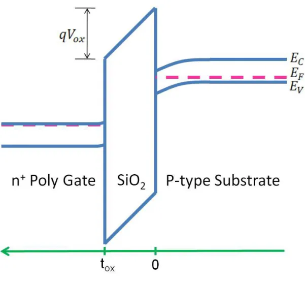
Fig. 1 Schematic of energy band diagram of the n+ poly-gate/SiO2/p-Si system. .. 25
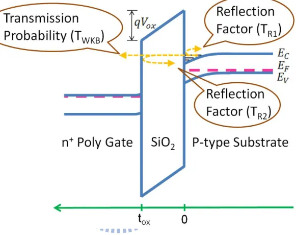
Fig. 2 Tunneling probability illustration. ... 26
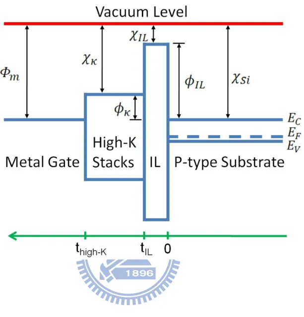
Fig. 3 Schematic of energy band diagram of the metal-gate/high-K/IL/p-Si system.
... 27
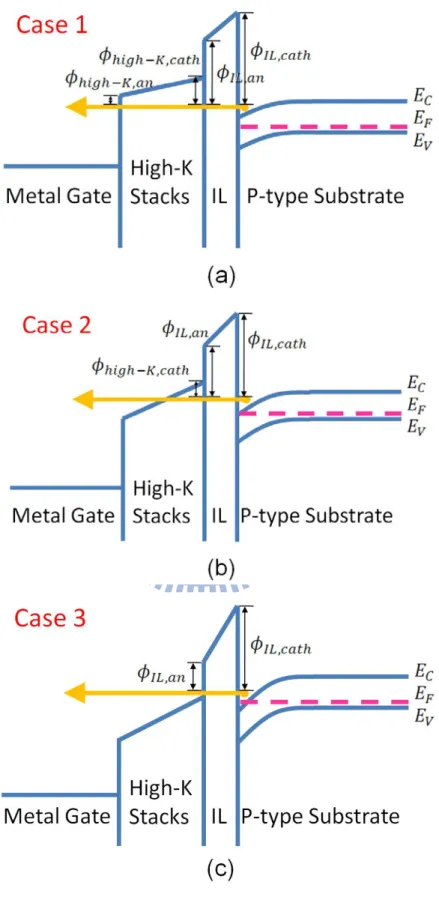
Fig. 4 Schematic description of three cases. (a)Case 1: direct tunneling through the
two layers. (b)Case 2: F-N tunneling through the high-K stacks. (c)Case 3:
direct tunneling through the IL ... 28
Fig. 5 Schematic of cross-sectional view of FinFET. FinFET with small fin width
is like a double gate structure. ... 29
Fig. 6 Comparison of the self-consistent Schrödinger-Poisson simulation and
analytical model for (a)surface potential and (b)electric field. ... 30
Fig. 7 The analytically calculated (lines) subband energy versus gate voltage and
the comparison with those (symbols) of the self-consistent
Schrödinger-Poisson simulation. (a)E(1,1); (b)E(2,1); (c)E(1,2); (d)E(2,2).
... 31
Fig. 8 Comparison of gate tunneling current versus gate voltage from the
self-consistent Schrödinger-Poisson (symbols) simulation and analytical
Fig. 9 The analytically calculated (lines) subband energy versus gate voltage and
the comparison with those (symbols) of the self-consistent
Schrödinger-Poisson simulation for EOT = 1.21nm, Φm = 4.4 eV, Nsub =
6x1017 cm-3, and tbody = 10 nm. ... 34
Fig. 10 The subband energy (best fitting) for different body thicknesses.
(a)tbody=10nm; (b)tbody=20nm; (c)tbody = 30nm; (d)tbody = 40nm; (e)tbody =
50nm. ... 35
Fig. 11 Subband fitting factors versus body thickness. Symbols are the values for
best fitting and lines are for linear fitting. ... 37
Fig. 12 The case of subband energy (linear relationship) for different body
thicknesses. (a)tbody=10nm; (b)tbody=20nm; (c)tbody = 30nm; (d)tbody = 40nm;
(e)tbody = 50nm. ... 38
Fig. 13 (a) Comparison of Ig(linear factors) with Ig(best factors) for tbody=10nm
and tbody=30nm. (b) Gate current change by linear and best factors. ... 40
Fig. 14 (a) The demonstration of three different tunneling regions. And Ig and
dlnIg/dVg versus Vg for (b) varying mk (c) varying Φk. ... 41
Fig. 15 The measured terminal current versus gate voltage for nFinFET. (a) terminal
current with source, drain and bulk tied to ground and (b) terminal current at
Fig. 16 Experimental (symbol) and simulated (line) Cg versus Vg for n-type FinFET.
The extracted process parameters are EOT = 0.8 nm, Φm = 4.6 eV and Nsub
= 1×10¹⁸
cm-3 ... 43
Fig. 17 Comparison of experimental (symbols) electron gate current with calculated
(lines) results. Fitting parameters are ϕk = 1.07 eV, mk = 0.02 mo, mIL = 1.22
mo, tk = 1.2 nm, and tIL = 1 nm. ... 44
Fig. 18 Schematic of the energy band diagram for (a) a linear gradual transition
layer and (b) a parabolic gradual transition layer. ... 45
Fig. 19 Comparison of experimental (symbols) electron gate current with calculated
(lines) results in the presence of a transition layer. (a) Linear gradual
transition layer, ϕk = 1.07 eV, mk = 0.02 mo, mIL = 0.8 mo, tk = 0.3nm , tmix =
1.31 nm, and tIL = 0.6 nm. (b) Parabolic gradual transition layer, ϕk = 1.07
eV, mk = 0.02 mo, mIL = 1.39 mo, tk = 0.4 nm , tmix = 1 nm, and tIL = 0.59
nm. ... 46
Fig. 20 Comparison of experimental (symbols) dlnIg/dVg versus Vg with calculated
(lines) results in the presence of a transition layer. The fitting parameters are:
(I)for no transition layer, mk = 0.02 m0, mIL = 1.22 m0, tk = 1.2 nm, and tIL =
1 nm; (II) for linear transition layer, mk = 0.02 m0, mIL = 0.8 m0, tk = 0.3 nm,
tmix = 1.31 nm, and tIL = 0.6 nm; (III) for linear transition layer, mk = 0.02
Chapter 1
Introduction
1.1 Background
Scaling of device is one of the main targets in IC fabrication technology. From
conventional SiO2 gate oxide MOSFET (metal-oxide-semiconductor field-effect
transistor) to high-K material gate dielectrics MOSFET, high-K devices are able to
reduce the gate leakage current. With the progressive scaling into 22nm and beyond,
short-channel effects (SCE) become a big issue. In order to suppress SCE, increasing
channel doping is one of the methods adopted in conventional planar devices. But
poor carrier mobility due to high channel doping is the weakness [1]. To overcome
the problem, several multiple gate structures have been proposed. Tri-gate device also
known as FinFET has been considered as potential candidate for 20 nm gate length. In
a FinFET, the gate drapes across the fin, giving the FinFET multiple gates compared
to the single gate of the planar transistor. So, the control of the gates on the channel in
a FinFET is stronger than in a conventional MOSFET as the gate voltage is applied
from several sides and not just from the top. One important feature of multiple gate
devices is that they do not need heavy channel doping to suppress short-channel
effects.
The MOSFET gate oxide thickness is rapidly approaching the direct tunneling
limit that ultimately leads to intolerably large standby power and impractical
applications. On the other hand, although high-K stacks exhibit lower gate tunneling
current, short-channel effect is more and more serious while pushing planar device
requires ultra-thin gate dielectrics, gate tunneling current is an important factor in
these devices, because it is related to the limitation of gate oxide scaling. So far, there
was no accurate model of FinFET gate tunneling current. Thus, the study in this
direction is necessary and important.
1.2 Arrangement of This Thesis
First of all, building tunneling current model for n-type FinFET is the main
purpose of this thesis. The direct tunneling physical model for oxide dielectric is
introduced in the first part of Chapter 2. This part includes four key parameters: the
inversion layer charge density, the electron impact frequency on interface, the WKB
transmission probability, and the reflection correction factor, as will be explained one
by one. Because the gate material of experimental FinFET device usually contains
high-K dielectric, modifying the model originally for conventional gate oxide SiO2 is
essential. Modified WKB transmission probability and reflection correction factor
both are introduced in the second part of Chapter 2. In order to calculate the electron
tunneling probability through the high-K stacks, the electron subband energy is
necessary to determine. In the third part of Chapter 2, we employ a simple method to
calculate subband energy.
Building the gate current model for FinFET is introduced in Chapter 3. It is divided
into three parts. First, because of the device structure change from planar to multiple
gate, full depletion situation needs to be considered in the double gate model.
Depletion charge density calculation is introduced in the first part. Next, the devices
of two gates induce confinement to the electrons while the body thickness is scaling
down. So the structure confinement makes a significant difference in calculated
dlnIg/dVg-Vg fitting is important for high-K stacks devices. We can find that it might
make an erroneous fitting result if the dlnIg/dVg fitting is not performed.
After the model is constructed, the experimental results about n-type FinFET are
shown in Chapter 4. By fitting experimental data, we can extract the process and
material parameters of the device. In the beginning, the gate current calculated by
analytical model deviates from experimental one. Modified tunneling models are
introduced by adding transition layer between the high-K dielectric and interfacial
layer. Linear transition layer and parabolic transition layer are the two models adopted
in this study. We can also prove that these models are valid for simulating the gate
current. The dlnIg/dVg fitting is also done to help determine accurately the gate
material parameters related to high-K dielectric. By all fittings and modifications, the
analytical model for tunneling current remains valid, especially above threshold of
Chapter 2
Physical Model for Planar FET
First, the principle of gate electron direct tunneling in an n+poly/SiO2/p-substrate
structure will be explained. Then, by substituting high-K for SiO2 as gate dielectric
material, a physical model of electron tunneling across high-K stacks is formed.
2.1 Tunneling Current Model for Oxide Dielectric
The basic band diagram of n+poly/SiO2/p-substrate is shown in Fig. 1. Quantum
mechanical calculation for the inversion layer in substrate and modified
Wentzel-Kramers-Brillouin (WKB) approximation for the transmission probability
across SiO2 layer are employed in this model [2],[3]. The direct tunneling electron
current model is made up of four key parameters: the inversion layer charge density,
the electron impact frequency on interface, the WKB transmission probability, and
specially, the reflection correction factor.
𝐽𝑔 = 𝑞𝑁𝑖,𝑗𝑓𝑗𝑇𝑊𝐾𝐵𝑇𝑅 (2-1) where
Jg is the electron tunneling current;
q is the elemental charge;
Ni,j is the inversion layer charge per unit area with jth subband in the ith valley;
fj is the electron impact frequency on SiO2/Si interface;
TWKB is the WKB transmission probability;
A. Inversion Layer Charge (Ni,j)
Using the density of states for a two-dimensional electron gas (2DEG) and
Fermi-Dirac statics, the inversion layer charge density of each energy subband can be
derived as
𝑁𝑖,𝑗 = �𝑘𝐵𝑇
𝜋ℏ2� 𝑔𝑖𝑚𝑑𝑖𝑙𝑛 �1 + 𝑒𝑥𝑝 �
𝐸𝐹−𝐸𝑖𝑗
𝑘𝐵𝑇 �� (2-2)
where gi is the degeneracy of the ith valley; mdi is the density of states electron
effective mass in the ith valley and Eij is the energy level of the jth subband in the ith
valley.
B. Electron Impact Frequency (fj)
The electron impact frequency can be described as [4]
𝑓𝑗 = �2 ∫ 1 𝜈𝑆𝑖⊥(𝑥) 𝑧𝑗 0 𝑑𝑥� −1 (2-3)
where zj epresents the classical turning point in silicon for electrons in each subband
and 𝜈𝑆𝑖⊥ the interface-normal group velocity component of electron wave packet, which can be expressed as
𝜈𝑆𝑖⊥(𝑥) = �2�𝐸𝑖𝑗−𝑞𝑉(𝑥)�
𝑚𝑧,𝑖 (2-4)
mz,i is the longitudinal or transverse effective mass in two or four fold valleys and V(x)
is the potential well which can be approximated as a triangle-like electrostatic potential:
𝑉(𝑥) =
𝜀𝑜𝑥𝐹𝑜𝑥𝑥𝜀𝑆𝑖 (2-5)
Substituting (2-4) and (2-5) into (2-3), then we can obtain the impact frequency
𝑓𝑗 = �2 ∫ 1 𝜈𝑆𝑖⊥(𝑥) 𝑧𝑗 0 𝑑𝑥� −1 = 𝑞𝜀𝑜𝑥|𝐹𝑜𝑥| 2𝜀𝑆𝑖 �2𝑚𝑧,𝑖𝐸𝑖𝑗� −12 (2-6)
C. WKB Transmission Probability (TWKB)
To calculate the tunneling probability across the oxide barrier in Fig. 2, a modified
WKB approximation is used. The modified WKB approximation includes TWKB and
TR [3],[4]. The former is the usual WKB tunneling probability, effective for smooth
potential barriers; the latter is a correction factor for reflections from potential
discontinuities. Both are combined in form:
𝑇 = 𝑇𝑊𝐾𝐵𝑇𝑅 (2-7) 𝑇𝑊𝐾𝐵 = 𝑒𝑥𝑝�−2 ∫ 𝜅(𝑥) 𝑑𝑥0𝑡𝑜𝑥 � (2-8) κ(x) is the magnitude of the carriers imaginary wave vector within the bandgap between the oxide layer
𝜅(𝑥) = �
2𝑚𝑜𝑥[𝐸−𝑞𝑉(𝑥)]ℏ2 (2-9)
Then substituting (2-9) into (2-8) yields
𝑇𝑊𝐾𝐵 = 𝑒𝑥𝑝 �−2 �∫ �2𝑚𝑜𝑥[𝐸−𝑞𝑉(𝑥)] ℏ2 𝑑𝑥 𝑡𝑜𝑥 0 �� = 𝑒𝑥𝑝 � 4�2𝑚𝑜𝑥�𝜙𝑎𝑛32 −𝜙 𝑐𝑎𝑡ℎ 3 2 � 3𝑞ℏ|𝐹𝑜𝑥| � (2-10)
𝜙𝑐𝑎𝑡ℎ and 𝜙𝑎𝑛 represent the magnitude of the electron (tunneling from the jth
subband in the ith valley) energy with reference to oxide conduction band in the
channel and in the gate, respectively. They are calculated by
𝑞𝜙𝑐𝑎𝑡ℎ = 𝑞𝜙𝑜𝑥 − 𝐸𝑖𝑗 (2-11) and
𝑞𝜙𝑎𝑛 = 𝑞𝜙𝑜𝑥 − 𝐸𝑖𝑗 − 𝑞𝐹𝑜𝑥𝑡𝑜𝑥 (2-12) where 𝜙𝑜𝑥 is the Si-SiO2 conduction band discontinuity.
The total energy is composed of transverse and longitudinal energies
𝐸 = ℏ
2�𝜅𝑥2+𝜅𝑦2�
In this equation, mt means the transverse effective mass and Ej is the energy in
longitudinal direction.
D. Reflection Correction Factor (TR)
Reflection factor is related to the type of material the wave penetrates. There are
two interfaces in n+poly-SiO2-p-substrate structure, Si/SiO2 and SiO2/n+poly. So the
reflection correction factor is
𝑇
𝑅= 𝑇
𝑅1𝑇
𝑅2=
4𝜈𝑆𝑖⊥(𝐸) × 𝜈𝑜𝑥(𝜙𝑐𝑎𝑡ℎ) 𝜈𝑆𝑖⊥2 (𝐸)+𝜈𝑜𝑥2 (𝜙𝑐𝑎𝑡ℎ)×
4𝜈𝑆𝑖⊥(𝐸+𝑞|𝐹𝑜𝑥|𝑡𝑜𝑥) × 𝜈𝑜𝑥(𝜙𝑎𝑛)
𝜈𝑆𝑖⊥2 (𝐸+𝑞|𝐹𝑜𝑥|𝑡𝑜𝑥)+𝜈𝑜𝑥2 (𝜙𝑎𝑛) (2-14)
where TR1 and TR2 are the reflection factors at the interface of Si/SiO2 and SiO2/n+poly,
respectively. 𝜈𝑆𝑖⊥(𝐸) is the group velocity of electrons incident at the silicon-oxide interface
𝜈
𝑆𝑖⊥(𝐸) = �
2𝐸𝑖𝑗𝑚𝑧 (2-15)
𝜈𝑜𝑥(𝜙𝑐𝑎𝑡ℎ) is the magnitude of the purely imaginary group velocity of electron at
the cathode side of SiO2:
𝜈
𝑜𝑥(𝜙
𝑐𝑎𝑡ℎ) =
1 ℏ 𝑑𝜙𝑐𝑎𝑡ℎ 𝑑𝜅𝑜𝑥=
ℏ2𝜅𝑜𝑥2 2𝑚𝑜𝑥 (2-16)On the other hand, 𝜈𝑆𝑖⊥(𝐸 + 𝑞|𝐹𝑜𝑥|𝑡𝑜𝑥) means the group velocity of electrons leaving the oxide-polygate interface and 𝜈𝑜𝑥(𝜙𝑎𝑛) is the magnitude of the purely imaginary group velocity of electron at the anode side of SiO2.
According to electron tunneling current model in (2-1), four important key
parameters have been introduced one by one, (2-2), (2-6), (2-10) and (2-14). As
electron tunneling is closely related to its subband energy, Eij, it will be introduced in
2.2 Modified Tunneling Current Model for High-K Gate Stacks
For highly scaled devices, thinner oxide induces a larger gate leakage current. In
order to maintain device performance in the scaling direction, use of high permittivity
is one of the solutions. In addition to dielectric layer change, poly gate is replaced by
metal gate and thereby the poly depletion can be eliminated. The band diagram of
metal gate/high-K/IL/p-substrate is shown in Fig. 3. Similarly, WKB approximation is
employed to build the tunneling current model, along with some parameters modified.
A. Modified WKB Transmission Probability for High-K Stacks (TWKB)
To calculate the tunneling probability in high-K case, electron not only goes
through the interfacial layer (IL) but also the high-K dielectric layer [4]. Consequently,
TWKB has two parts in terms of interfacial layer and high-K dielectric:
𝑇𝑊𝐾𝐵 = 𝑒𝑥𝑝 ��−2 ∫ 𝜅(𝑥) 𝑑𝑥0𝑡𝐼𝐿 � + �−2 ∫𝑡𝑡ℎ𝑖𝑔ℎ−𝐾𝜅(𝑥) 𝑑𝑥
𝐼𝐿 �� (2-17)
The above equation can apply to high-K stacks, but it is just one of the several cases.
The band diagram changes with varying gate bias voltage, meaning that lower
tunneling barrier height corresponds to higher gate voltage. Three cases are shown in
Fig. 4. 𝜙𝐼𝐿,𝑐𝑎𝑡ℎ is denoted as the barrier height for tunneling electrons with reference to oxide conduction band at IL/p-substrate interface and 𝜙𝐼𝐿,𝑎𝑛 is the barrier height at high-K/IL interface in interfacial layer. 𝜙ℎ𝑖𝑔ℎ−𝐾,𝑐𝑎𝑡ℎ and 𝜙ℎ𝑖𝑔ℎ−𝐾,𝑎𝑛 are also the barrier heights with the former at high-K/IL interface in high-K dielectric and the
latter at metal-gate/high-K interface. They are calculated by
𝑞𝜙𝐼𝐿,𝑐𝑎𝑡ℎ = 𝑞𝜙𝐼𝐿− 𝐸𝑖𝑗 (2-18) 𝑞𝜙𝐼𝐿,𝑎𝑛 = 𝑞𝜙𝐼𝐿− 𝐸𝑖𝑗 − 𝑞𝐹𝐼𝐿𝑡𝐼𝐿 (2-19) 𝑞𝜙ℎ𝑖𝑔ℎ−𝐾,𝑐𝑎𝑡ℎ = 𝑞𝜙ℎ𝑖𝑔ℎ−𝐾 − 𝐸𝑖𝑗 − 𝑞𝐹𝐼𝐿𝑡𝐼𝐿 (2-20) 𝑞𝜙ℎ𝑖𝑔ℎ−𝐾,𝑎𝑛 = 𝑞𝜙ℎ𝑖𝑔ℎ−𝐾− 𝐸𝑖𝑗 − 𝑞𝐹𝐼𝐿𝑡𝐼𝐿− 𝑞𝐹ℎ𝑖𝑔ℎ−𝐾𝑡ℎ𝑖𝑔ℎ−𝐾 (2-21)
By Gauss’ law we can get Vhigh-K (potential drop across high-K dielectric) easily, 𝐹𝐼𝐿 = 𝑉𝐼𝐿 𝑡𝐼𝐿 (2-22) 𝐹ℎ𝑖𝑔ℎ−𝐾 = 𝑉ℎ𝑖𝑔ℎ−𝐾 𝑡ℎ𝑖𝑔ℎ−𝐾 = 𝐹𝐼𝐿 𝜀𝐼𝐿 𝜀ℎ𝑖𝑔ℎ−𝐾 (2-23)
The three tunneling cases can be classified by defining the underlying conditions:
Case 1 --- 𝜙𝐼𝐿,𝑐𝑎𝑡ℎ > 0, 𝜙𝐼𝐿,𝑎𝑛 > 0, 𝜙ℎ𝑖𝑔ℎ−𝐾,𝑐𝑎𝑡ℎ > 0 𝑎𝑛𝑑 𝜙ℎ𝑖𝑔ℎ−𝐾,𝑎𝑛> 0 Case 2 --- 𝜙𝐼𝐿,𝑐𝑎𝑡ℎ > 0, 𝜙𝐼𝐿,𝑎𝑛 > 0, 𝜙ℎ𝑖𝑔ℎ−𝐾,𝑐𝑎𝑡ℎ > 0 𝑎𝑛𝑑 𝜙ℎ𝑖𝑔ℎ−𝐾,𝑎𝑛≤ 0 Case 3 --- 𝜙𝐼𝐿,𝑐𝑎𝑡ℎ > 0, 𝜙𝐼𝐿,𝑎𝑛 > 0, 𝜙ℎ𝑖𝑔ℎ−𝐾,𝑐𝑎𝑡ℎ ≤ 0 𝑎𝑛𝑑 𝜙ℎ𝑖𝑔ℎ−𝐾,𝑎𝑛≤ 0
Substituting the three cases into (2-17), the three conditions of tunneling probability
are Case 1 --- 𝑇𝑊𝐾𝐵 = 𝑒𝑥𝑝 � 4�2𝑚𝐼𝐿�𝜙𝐼𝐿,𝑎𝑛 3 2 −𝜙 𝐼𝐿,𝑐𝑎𝑡ℎ 3 2 � 3𝑞ℏ|𝐹𝐼𝐿| � 𝑒𝑥𝑝 � 4�2𝑚ℎ𝑖𝑔ℎ−𝐾�𝜙ℎ𝑖𝑔ℎ−𝐾,𝑎𝑛 3 2 −𝜙 ℎ𝑖𝑔ℎ−𝐾,𝑐𝑎𝑡ℎ 3 2 � 3𝑞ℏ�𝐹ℎ𝑖𝑔ℎ−𝐾� � Case 2 --- 𝑇𝑊𝐾𝐵 = 𝑒𝑥𝑝 ⎣ ⎢ ⎢ ⎢ ⎡4�2𝑚𝐼𝐿�𝜙𝐼𝐿,𝑎𝑛 3 2 − 𝜙 𝐼𝐿,𝑐𝑎𝑡ℎ 3 2 � 3𝑞ℏ|𝐹𝐼𝐿| ⎦ ⎥ ⎥ ⎥ ⎤ 𝑒𝑥𝑝 ⎣ ⎢ ⎢ ⎢ ⎡4�2𝑚ℎ𝑖𝑔ℎ−𝐾�0 − 𝜙ℎ𝑖𝑔ℎ−𝐾,𝑐𝑎𝑡ℎ 3 2 � 3𝑞ℏ�𝐹ℎ𝑖𝑔ℎ−𝐾� ⎦ ⎥ ⎥ ⎥ ⎤ Case 3 --- 𝑇𝑊𝐾𝐵 = 𝑒𝑥𝑝 � 4�2𝑚𝐼𝐿 �𝜙𝐼𝐿,𝑎𝑛 3 2 −𝜙 𝐼𝐿,𝑐𝑎𝑡ℎ 3 2 � 3𝑞ℏ|𝐹𝐼𝐿| � (2-24)
B. Modified Reflection Correction Factor for High-K Stacks (TR)
unity for metal/high-K dielectric interface and for the interface of high-K gate stacks,
so we only consider the reflection at the Si/IL interface in our model. Therefore, the
correcting TR for high-K stacks is as follows:
𝑇
𝑅=
4𝜈𝑆𝑖⊥(𝐸) × 𝜈𝐼𝐿�𝜙𝐼𝐿,𝑐𝑎𝑡ℎ�𝜈𝑆𝑖⊥2 (𝐸)+𝜈𝐼𝐿2 �𝜙𝐼𝐿,𝑐𝑎𝑡ℎ� (2-25)
2.3 Subband Energy Calculation
In this part, the method of calculating the electron subband energy will be
introduced. We employ a simplified method to calculate the quantum mechanical
effect in the inversion layer of a p-type Si substrate. Four physical values are
estimated in this method; they are the charge densities in depletion and inversion, the
depletion region band bending, and the inversion layer band bending. Those
characteristic parameters of p-type substrate under the inversion conditions are
denoted
𝑁𝑑𝑒𝑝 is the depleted space charge;
𝑁𝑖𝑛𝑣 is the interfacial inversion charge;
𝜙𝑠 is the semiconductor surface potential or surface band bending;
𝜙𝑑𝑒𝑝 is the band bending due to the depletion charge.
One assumption needs to be used to while simplifying the subband energy model:
the quantum confinement phenomenon of the MOS structure can be treated in a
triangular well approximation, so the potential at the semiconductor surface layer
follows a linear variation. This approximation has been shown to describe the electron
behavior adequately as validated by self-consistent Schrödinger and Poisson
equations solving.
charge each are related to corresponding surface band bending. The total charge per
unit area (𝑄) below the MOS gate is the sum of the inversion electron charge(𝑁𝑖𝑛𝑣) and the depletion charge(𝑁𝑑𝑒𝑝). The total charge from the law of electrostatics is
𝑁𝑖𝑛𝑣+ 𝑁𝑑𝑒𝑝 = 𝑄(𝜙𝑠) (2-26) First, the surface potential is essential for calculating the total charge.
𝜙𝑑𝑒𝑝 = 𝜙𝑠−𝑞𝑁𝑠𝑧̅𝑞𝑚
𝜀𝑆𝑖𝜀0 −
𝑘𝑇
𝑞 (2-27)
The second term of the right side of (2-27) stems from the influence of inversion
charge 𝑁𝑖𝑛𝑣; the third term 𝑘𝑇
𝑞 from the gradual transition of the space charge region
into the substrate, and the term 𝜙𝑑𝑒𝑝 due to the space charge 𝑁𝑑𝑒𝑝.
𝑁
𝑑𝑒𝑝= �
2𝜀𝑆𝑖𝜀0𝜙𝑑𝑒𝑝𝑁𝑠𝑢𝑏𝑞 (2-28)
𝑧̅𝑞𝑚 in (2-27) is the average equivalent widths of the quantum confined electron gas,
as described by
𝑧̅
𝑞𝑚= ∑
𝑧𝑖𝑗𝑁𝑖𝑗𝑁𝑖𝑛𝑣
𝑖,𝑗
(2-29)
𝑧𝑖𝑗 is weighted with the corresponding subband occupation factor Nij, thus
constituting the mean quantum mechanical channel width 𝑧̅𝑞𝑚. In this case, the wave functions are given by Airy functions. So the mean subband width 𝑧𝑖𝑗 is calculated by
𝑧
𝑖𝑗= ∫�𝛹𝑖𝑗(𝑧)�
2𝑧 𝑑𝑧 =
2𝐸𝑖𝑗𝜀𝑆𝑖3𝑞𝜀𝑜𝑥𝐸𝑜𝑥
(2-30)
The energy eigenvalues Eij can be expressed as
𝐸
𝑖𝑗= �
ℏ2 2𝑚𝑖�
1 3�
3𝜋𝑞𝜀𝑜𝑥𝐹𝑜𝑥�𝑗− 1 4� 2𝜀𝑆𝑖�
2 3 (2-31)where mi is the normal mass for two fold valley or four fold valley, Fox is the oxide
𝑁𝑖𝑗 = ∫ 𝐷𝑖(𝐸)𝑓(𝐸)𝑑𝐸 = 𝑚𝑑𝑖 𝜋ℏ2𝑙𝑛 �1 + 𝑒𝑥𝑝 � 𝐸𝐹−𝐸𝑖𝑗 𝑘𝑇 �� ∞ 𝐸𝑖𝑗 (2-32)
where Di(E) is the density of states of the subband for two dimentional gas and f(E) is
Chapter 3
Physical Model for FinFET
In this chapter, multiple gate devices are introduced, including gate tunneling
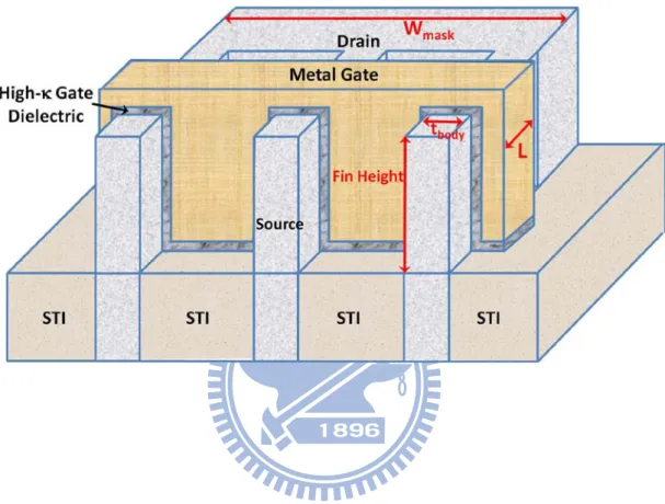
current and electron energy in double gate and FinFET devices. Fig. 5 reveals that the
width of FinFET is insignificant compared to the whole gate length (WFin+2HFin), we
can regard FinFET as double gate structure.
There are some changes to the tunneling model because of the different physical
structural change from planar to double gate. The equations of depletion charge
density and subband energy have to be modified since the Si body part is affected by
both the front and back gate.
3.1 Depletion Charge Density Calculation
It is a significant improvement in the double gate structure that the substrate is
controlled by two gates (front gate and back gate). Owing to its capability of
sensitively influencing the channel, to suppress the short channel effects, the body
doping can be decreased. While body thickness is reduced, full depletion in the body
happens under the small gate voltage condition. So the task to calculate depletion
charge density needs to be considered in two distinct situations:
Case 1 ---
𝐼𝑓 �
2𝜀𝑆𝑖𝜀0𝜙𝑑𝑒𝑝𝑁𝑠𝑢𝑏 𝑞<
𝑁𝑠𝑢𝑏𝑡𝑏𝑜𝑑𝑦 2⟹ 𝑁
𝑑𝑒𝑝= �
2𝜀𝑆𝑖𝜀0𝜙𝑑𝑒𝑝𝑁𝑠𝑢𝑏 𝑞 Case 2 ---𝐼𝑓 �
2𝜀𝑆𝑖𝜀0𝜙𝑑𝑒𝑝𝑁𝑠𝑢𝑏 𝑞>
𝑁𝑠𝑢𝑏𝑡𝑏𝑜𝑑𝑦 2⟹ 𝑁
𝑑𝑒𝑝=
𝑁𝑠𝑢𝑏𝑡𝑏𝑜𝑑𝑦 2Case 1 is the condition that the channel works in depletion region. In this case, the
attributed by the doping concentration are totally depleted. Therefore, the depletion
charge density is equal to half of the body doping charge density. It is not the total
charge density because one gate just controls half of the charge in the channel. As
long as the body doping is large enough, full depletion is going to happen later due to
large gate voltage needed.
3.2 Subband Energy Calculation for FinFET
In double gate devices, gate leakage current and subthreshold leakage both are
affected by the quantization of electron energy. Owing to small body thickness,
structure confinement needs to be considered in calculating electron energy. Surface
band bending changes the electric field in the substrate, so field confinement is
another factor [5],[6]. The energy level associated with the jth subband of the ith
valley (longitudinal or transverse) is given by
𝐸
𝑖𝑗= �
ℏ 2 2𝑚𝑖�
1 3�
3𝜋𝑞𝜀𝑜𝑥𝐹𝑜𝑥�𝑗− 1 4� 2𝜀𝑆𝑖�
𝜂+
8𝑚𝑗2(2𝜋ℏ)2 𝑖𝑡𝑏𝑜𝑑𝑦2 (4-1)The first term in (4-1) is field confinement factor and the second is structure
confinement one. η is a fitting factor (theoretically ≈ 2/3), mi is the electron effective
mass at ith valley and tbody is the thickness of body between front gate dielectric and
back gate dielectric.
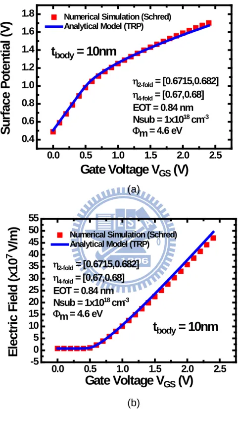
From Fig. 6, it can be observed that, due to the absence of the bulk charge in the
double gate device, the surface electric field is negligible below threshold. Therefore,
in the double gate device, the electron quantization occurs principally due to the
structural confinement below threshold. However, above threshold, an increase in
gate voltage increases the electric field (due to higher inversion charge) which also
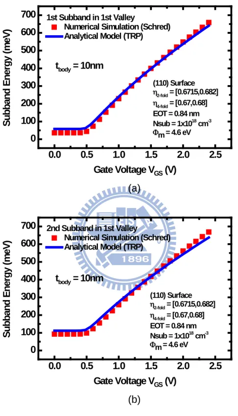
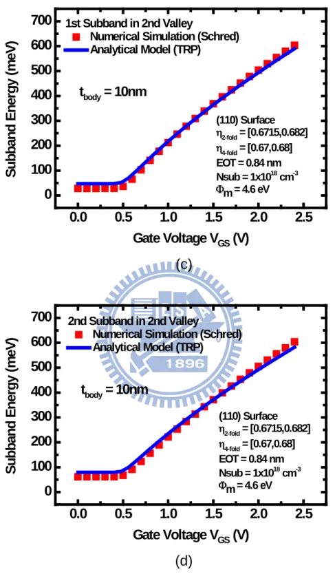
(Fig. 7). Evidence to validate the analytical model is given in Fig. 8, which shows that
the gate current density values obtained from the numerical simulation and the
analytical model are equal. Fig. 9 shows the subband energy in varying body doping
concentration, effective oxide thickness and metal work function. We can find that no
matter how the characteristics of the device change, the subband energies from
analytical model and numerical simulation are nearly identical to each other, valid in
the same fitting factors. Only the altered body thickness can change fitting factors.
We obtain the four subband fitting factors of 0.6715, 0.682, 0.67, and 0.68 for 10nm
tbody (Fig. 10). These fitting factors all approach 2/3 as mentioned in [3],[5],[6].
The subband energy for body thicknesses from 10nm to 50nm all are closely
comparable between analytical model and numerical simulation (Fig. 10). Fitting
factor versus body thickness is plotted in Fig. 11. The fitting factors symbols for
different oxide thicknesess represent the best fitting situations in Fig. 10. We can find
that the fitting factor decreases as oxide thickness increases. It can be observed from
Fig. 11 that data points are distinguished into two parts, with the first subband
below second subband. All of the fitting factors lead to a linear relationship. Now, we
have two sets of fitting factors, best fitting factors and linear fitting factors. The
former is shown in Fig. 11 by discrete points and the latter by solid linear lines. Then,
by using the fitting factors from the linear relation, the resulting subband energy does
match the simulated value (Fig. 12). In order to testify the validity of the linear fitting
factors, gate current from best factors and linear factors is shown in Fig. 13. The gate
current curves in best and linear factors are almost equal as shown in Fig. 13(a) for
body thicknesses of 10 and 30 nm. The gate current values for body thickness of
20nm, 40nm and 50nm are not shown explicitly but very small gate current change
established by means of the linear equation of fitting factors shown in Fig. 11.
3.3 Parameters in FinFET Gate Tunneling Current Model
Transmission probability calculation is the most important part in this physical
model. According to (2-24), 𝑚𝐼𝐿, 𝑚ℎ𝑖𝑔ℎ−𝐾, 𝜙𝐼𝐿,𝑎𝑛, 𝜙𝐼𝐿,𝑐𝑎𝑡ℎ, 𝜙ℎ𝑖𝑔ℎ−𝐾,𝑎𝑛, 𝜙ℎ𝑖𝑔ℎ−𝐾,𝑐𝑎𝑡ℎ and 𝐹𝐼𝐿, 𝐹ℎ𝑖𝑔ℎ−𝐾 are essential for resolving this equation. How to find the tunneling effective masses in interfacial layer (𝑚𝐼𝐿) and high-K layer (𝑚ℎ𝑖𝑔ℎ−𝐾) will be explained later. In order to obtain 𝜙𝐼𝐿,𝑎𝑛, 𝜙𝐼𝐿,𝑐𝑎𝑡ℎ, 𝜙ℎ𝑖𝑔ℎ−𝐾,𝑎𝑛 and 𝜙ℎ𝑖𝑔ℎ−𝐾,𝑐𝑎𝑡ℎ, 𝜙𝐼𝐿 and 𝜙ℎ𝑖𝑔ℎ−𝐾 are the two parameters used in the equations from (2-18) to (2-21). The electric field in interfacial layer (𝐹𝐼𝐿) and high-K dielectric (𝐹ℎ𝑖𝑔ℎ−𝐾) are defined in (2-22) and (2-23).
According to [8],[9], a method of extracting gate material parameters has been
proposed, as long as gate current is dominated by direct tunneling or
Fowler-Nordheim tunneling (F-N tunneling) from the plot of dlnIg/dVg versus Vg
(Fig. 14). The transition of direct tunneling and F-N tunneling across high-K has a
peak of dlnIg/dVg, and as a consequence, the position of the peak over can provide a
direct estimate of metal work function and high-K electron affinity. From Fig. 14(b)
and Fig. 14(c), 𝜙ℎ𝑖𝑔ℎ−𝐾 determines the peak position; 𝑚ℎ𝑖𝑔ℎ−𝐾 determines the peak height. So, adjusting 𝜙ℎ𝑖𝑔ℎ−𝐾 can shift the fitting curve of dlnIg/dVg versus Vg until the position of the peak is the same as the experimental value. Then, adjusting
𝑚ℎ𝑖𝑔ℎ−𝐾 can change the height of dlnIg/dVg peak until it approaches the
experimental value. The parameters related to high-K are determined from the above
method. Then, band offset with respect to silicon and the tunneling effective mass in
interfacial layer, 𝜙𝐼𝐿 and 𝑚𝐼𝐿, can be extracted by fitting gate current versus gate voltage. Higher 𝜙𝐼𝐿 decreases the gate current because the electric barrier height can
need more energy to tunnel across the interfacial layer, leading to gate tunneling
current drop. Higher 𝑚𝐼𝐿 also decreases the gate current because the electric effective mass can significantly affect the tunneling probability as shown in equation
(2-24). The differential value of the band offset between the anode side and cathode
side is negative. It means that the higher the effective mass is, the less likely the
tunneling occurs. We can therefore extract the relevant HKMG material parameters
by combining conventional Cg-Vg and Ig-Vg curve fittings with the new
Chapter 4
Metal-Gate/High-K FinFET:
Experiment and Fitting
The experimental devices were n-type FinFET with metal-gate/high-K/IL system,
as schematically depicted in Fig. 3 in terms of energy band diagram in flat-band
condition. Because of the small ratio of top gate width to total fin width, we can
regard the FinFET structure as double gate structure, as shown in Fig. 5.
The electron tunneling current from inversion layer was measured with source,
drain and bulk tied to ground. The measured terminal current is shown in Fig. 15(a).
The case of Vd = 0.05V is shown in Fig. 15(b). The following process parameters
were obtained by Cg-Vg fitting using the Schrödinger-Poisson equation solver Schred
[10], as depicted in Fig. 16. The results are that the metal work function Φ𝑚 is 4.6eV, the EOT is 0.8nm, and the p-type substrate doping concentration 𝑁𝑠𝑢𝑏 is 1×1018 cm-3. Then, we took the permittivity of HfO2 bases high-K (εk) as the literature value of 22
ε0 [11] and to meet EOT (0.8nm), the permittivity of IL (εIL) is determined to be 6.6 ε0.
Corresponding band offsets of IL (ϕIL) to silicon conduction and valence band are
therefore 2.44 eV [12].
The gate current was measured with source, drain, and bulk tied to the ground. The
measured result has been depicted in Fig. 15(a) versus Vg. In the gate current fitting,
the actual electron tunneling current is close to the electron tunneling current from the
first and second subband. For the purpose of saving the computation time, we just
calculate the first and second subband in this work. Many simplifications are
employed in our tunneling simulation, but the results are reasonable as compared with
WKB approximation of electron transmission probability through the high-K stacks.
From the fitting result in Fig. 17, the simulation by our model is not correct for the
gate bias below threshold voltage. The reason for this failure can be attributed to the
fact that the gate current is not dominated by direct tunneling in threshold region but
our tunneling current model is limited to pure tunneling. Another drawback is that a
serious deviation occurs at high gate voltage. This is due to the very large difference
of permittivity between high-K dielectric (22 ε0) and IL (6.6 ε0). Thus, a gradual
transition (intermixing) layer between high-K dielectric and IL needs to be considered
in the calculation. The tunneling effective masses of transition layer can be assumed
to be linear or parabolic type, as schematically plotted in Fig. 18. The current fitting
results are shown in Fig. 19. We find that fitting quality can be improved with the
transition layer included, especially for the parabolic one. Although the simulator
cannot work in subthreshold region, WKB approximation still show good agreements
with the experimental curve even when the gate bias is large enough. The following
discussion focuses on the range of the current closely falling the range of gate bias
larger than the threshold voltage.
Now, all the model parameters are known, except 𝜙ℎ𝑖𝑔ℎ−𝐾, 𝑚𝐼𝐿 and 𝑚ℎ𝑖𝑔ℎ−𝐾. In order to find the parameters related to high-K dielectric, dlnIg/dVg fitting is used
again. As mentioned in Chapter 3.3, 𝜙ℎ𝑖𝑔ℎ−𝐾 and 𝑚ℎ𝑖𝑔ℎ−𝐾 dominate the position of the peak and the height of the peak in the dlnIg/dVg versus Vg, respectively. 𝜙ℎ𝑖𝑔ℎ−𝐾 is adjusted first until the position of the dlnIg/dVg peak approaches the experimental
data (~1.5V). Next, 𝑚ℎ𝑖𝑔ℎ−𝐾 is changed until the height of the dlnIg/dVg peak closely meets the experimental data (~7V-1). The fitting result is shown in Fig. 20 and the extracted results are 𝜙ℎ𝑖𝑔ℎ−𝐾 = 1.07 𝑒𝑉 and 𝑚ℎ𝑖𝑔ℎ−𝐾= 0.02𝑚0.
fitting. The experimental and fitting gate current without transition layer are plotted in
Fig. 17 and Fig. 19 with linear and parabolic transition layer. In the Ig-Vg fitting, the
gate current does not change by adjusting the value of 𝜙ℎ𝑖𝑔ℎ−𝐾 or 𝑚ℎ𝑖𝑔ℎ−𝐾 in case 3 (only direct tunneling through the IL). No matter how the high-K dielectric
Chapter 5
Conclusion
FinFET gate current model has been established by modifying the gate current
model for metal-gate/high-K device. Because of the small ratio between top width and
the whole width, double gate tunneling current model can be applied to FinFET. A
compact model for the structure that is similar to double gate devices has been
established.
As the width of FinFET is insignificant compared to the whole gate length, the
fitting factor of electron subband energy has regularity in the region of body thickness
between 10nm and 50nm. When the body thickness is fixed in double gate structure,
the fitting factor does not need to adjust. The model can straightforwardly yield the
correct subband energy. For the case of varying body thickness, we can obtain a
reasonable fitting factor from the linear relationship. Conventionally, Ig-Vg and
Cg-Vg curve fittings are used to extract the parameters. Because of the apparent
deviation of gate current fitting at high voltage, transition layer between the high-K
dielectric and the interfacial layer is incorporated. Linear and parabolic-type transition
layer are adopted in the model. By taking into account the transition layer, the gate
tunneling current fitting and dlnIg/dVg fitting can be significantly improved. It is
found that parabolic transition layer can produce a better agreement with experiment
than linear transition layer.
A peak of dlnIg/dVg indicates a transition of direct tunneling and F-N tunneling
across a high-K part, and as a consequence, the position of the dlnIg/dVg peak over
systematically constructed a new fitting scheme over the dlnIg/dVg versus Vg curve,
along with the combination of Cg-Vg and Ig-Vg fittings. In addition, we have
demonstrated that the conventional method without the dlnIg/dVg fitting might lead
to erroneous results, Thus, the dlnIg/dVg fitting should be taken into account in the
References
[ 1 ] Amitava DasGupta, “Multiple Gate MOSFETs: The Road to Future,” in
Proceedings of the 2007 International Workshop on the Physics of Semiconductor Devices (IWPSD), pp. 96-101, Sep. 2007.
[ 2 ] Leonard F. Register, Elyse Rosenbaum, and Kevin Yang, “Analytic model for
direct tunneling current in polycrystalline silicon-gate metal-oxide-semi-
conductor devices,” Appl. Phys. Lett., vol. 74, no. 3, pp. 457-459, Jan. 1999.
[ 3 ] Kuo-Nan Yang, Huan-Tsung Huang, Ming-Chin Chang, Che-Min Chu, Yuh-Shu
Chen, Ming-Jer Chen, Yeou-Ming Lin, Mo-Chiun Yu, Simon M. Jang, Douglas
C. H. Yu, and M. S. Liang, “A physical model for hole direct tunneling current
in p+ poly-gate PMOSFETs with ultrathin gate oxides,” IEEE Trans. Electron
Devices, vol. 47, no. 11, pp. 2161-2166, Nov. 2000.
[ 4 ] Yijie Zhao and Marvin H. White, “Modeling of direct tunneling current through
interfacial oxideand high-K gate stacks,” Solid-State Electronics, vol.48, no.
10-11, pp. 1801-1807, Dec. 2003.
[ 5 ] Saibal Mukhopadhyay, Keunwoo Kim, Ching Te Chuang, and Kaushik Roy,
“Modeling and Analysis of Leakage Currents in Double-Gate Technologies,”
IEEE Trans. Computer–Aided Design of Integrated Circuits and Systems, vol. 25, no. 10, pp. 2052-2061, Oct. 2006.
[ 6 ] Saibal Mukhopadhyay, Keunwoo Kim, Jae-Joon Kim, Shih-Hsien Lo, Rjiv V.
Joshi, Ching-Te Chuang, and Kaushik Roy, “Estimation of gate-to-channel
tunneling current in ultra-thin oxide sub-50 nm double gate devices,”
[ 7 ] Leland Chang, Kevin J. Yang, Yee-Chia Yeo, Igor Polishchuk, Tsu-Jae King,
and Chenming Hu, “Direct-Tunneling Gate Leakage Current in Double-Gate and
Ultrathin Body MOSFETs,” IEEE Trans. Electron Devices, vol. 49, no. 12, pp.
2288-2295, Dec. 2002.
[ 8 ] Sufi Zafar, Cyril Cabral, Jr., R. Amos, and A. Callegari, “A method for
measuring barrier heights, metal work functions and fixed charge densities in
metal/SiO2/Si capacitors,” Appl. Phys. Lett., vol. 80, no. 25, pp. 4858-4860, Jun.
2002.
[ 9 ] Chih-Yu Hsu, Hua-Gang Chang, and Ming-Jer Chen, “A Method of Extracting
Metal-Gate High-k Material Parameters Featuring Electron Gate Tunneling
Current Transition,” IEEE Trans. Electron Devices, vol. 58, no. 4, pp. 953-959,
Apr. 2011.
[ 10 ] Schred. [Online]. Available: http://nanohub.org/resources/schred
[ 11 ] Y. T. Hou, M. F. Li, H. Y. Yu, and D. L. Kwong, “Modeling of tunneling
currents through HfO2 and (HfO2)x(Al2O3)1-x gate stacks,” IEEE Electron
Device Lett., vol. 24, no. 2, pp. 96-98, Feb. 2003.
[ 12 ] Hongyu Yu, Yong-Tian Hou, Ming-Fu Li, and Dim-Lee Kwong, “Investigation
of Hole Tunneling Current Through Ultrathin Oxynitride/Oxide Stack Gate
Dielectrics for p-MOSFETs,” IEEE Trans. Electron Devices, vol. 49, no. 7, pp.
Fig. 4 Schematic description of three cases. (a)Case 1: direct tunneling through the two layers. (b)Case 2: F-N tunneling through the high-K stacks. (c)Case 3: direct tunneling through the IL
Fig. 5 Schematic of cross-sectional view of FinFET. FinFET with small fin width is like a double gate structure.
(a)
(b)
Fig. 6 Comparison of the self-consistent Schrödinger-Poisson simulation and analytical model for (a)surface potential and (b)electric field.
0.0
0.5
1.0
1.5
2.0
2.5
0.4
0.6
0.8
1.0
1.2
1.4
1.6
1.8
Numerical Simulation (Schred)Analytical Model (TRP)
η
2-fold= [0.6715,0.682]
η
4-fold= [0.67,0.68]
EOT = 0.84 nm
Nsub = 1x10
18cm
-3Φm = 4.6 eV
t
body= 10nm
S
u
rf
ace P
o
ten
ti
al
(
V
)
Gate Voltage V
GS(V)
0.0
0.5
1.0
1.5
2.0
2.5
-5
0
5
10
15
20
25
30
35
40
45
50
55
Gate Voltage V
GS(V)
η
2-fold= [0.6715,0.682]
η
4-fold= [0.67,0.68]
EOT = 0.84 nm
Nsub = 1x10
18cm
-3Φm = 4.6 eV
E
lect
ri
c F
iel
d
(
x10
7V/
m
)
Numerical Simulation (Schred) Analytical Model (TRP)
(a)
(b)
Fig. 7-1 The analytically calculated (lines) subband energy versus gate voltage and the comparison with those (symbols) of the self-consistent Schrödinger-Poisson simulation. (a)E(1,1); (b)E(2,1); (c)E(1,2); (d)E(2,2).
0.0
0.5
1.0
1.5
2.0
2.5
0
100
200
300
400
500
600
700
S
ubba
nd E
ne
rgy
(
m
e
V
)
Gate Voltage V
GS(V)
(110) Surface η2-fold = [0.6715,0.682] η4-fold = [0.67,0.68] EOT = 0.84 nm Nsub = 1x1018 cm-3 Φm = 4.6 eV 1st Subband in 1st ValleyNumerical Simulation (Schred) Analytical Model (TRP)
t
body= 10nm
0.0
0.5
1.0
1.5
2.0
2.5
0
100
200
300
400
500
600
700
(110) Surface η2-fold = [0.6715,0.682] η4-fold = [0.67,0.68] EOT = 0.84 nm Nsub = 1x1018 cm-3 Φm = 4.6 eV 2nd Subband in 1st ValleyNumerical Simulation (Schred) Analytical Model (TRP)
S
ubba
nd E
ne
rgy
(
m
e
V
)
Gate Voltage V
GS(V)
t
body= 10nm
(c)
(d)
Fig. 7-2 The analytical calculated (lines) subband energy versus gate voltage and the comparison with those (symbols) of the self-consistent Schrödinger-Poisson simulation. (a)E(1,1); (b)E(2,1); (c)E(1,2); (d)E(2,2).
0.0
0.5
1.0
1.5
2.0
2.5
0
100
200
300
400
500
600
700
(110) Surface η2-fold = [0.6715,0.682] η4-fold = [0.67,0.68] EOT = 0.84 nm Nsub = 1x1018 cm-3 Φm = 4.6 eV 1st Subband in 2nd ValleyNumerical Simulation (Schred) Analytical Model (TRP)
S
ubba
nd E
ne
rgy
(
m
e
V
)
Gate Voltage V
GS(V)
t
body= 10nm
0.0
0.5
1.0
1.5
2.0
2.5
0
100
200
300
400
500
600
700
2nd Subband in 2nd ValleyNumerical Simulation (Schred) Analytical Model (TRP) (110) Surface η2-fold = [0.6715,0.682] η4-fold = [0.67,0.68] EOT = 0.84 nm Nsub = 1x1018 cm-3 Φm = 4.6 eV
S
ubba
nd E
ne
rgy
(
m
e
V
)
Gate Voltage V
GS(V)
t
body= 10nm
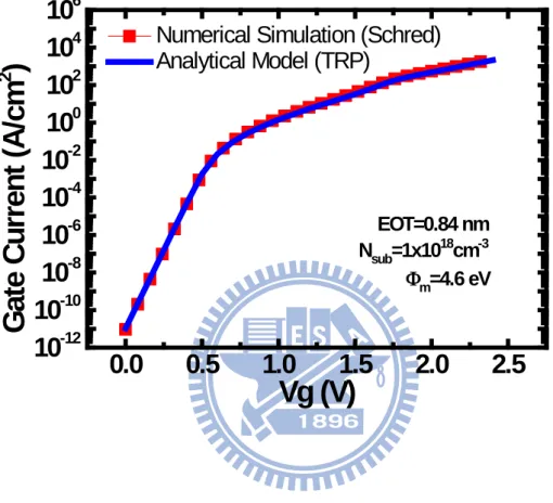
Fig. 8 Comparison of gate tunneling current versus gate voltage from the self-consistent Schrödinger-Poisson (symbols) simulation and analytical model (lines).
0.0
0.5
1.0
1.5
2.0
2.5
10
-1210
-1010
-810
-610
-410
-210
010
210
410
6 EOT=0.84 nm Nsub=1x1018cm-3 Φm=4.6 eVG
at
e C
u
rr
en
t
(A/
c
m
2)
Vg (V)
Numerical Simulation (Schred)
Analytical Model (TRP)
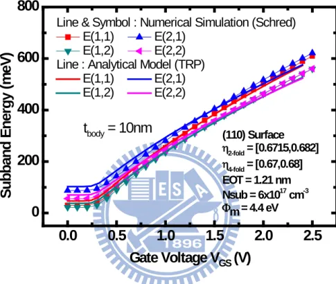
Fig. 9 The analytically calculated (lines) subband energy versus gate voltage and the comparison with those (symbols) of the self-consistent Schrödinger-Poisson simulation for EOT = 1.21nm, Φm = 4.4 eV, Nsub = 6x1017 cm-3, and tbody = 10 nm.
0.0
0.5
1.0
1.5
2.0
2.5
0
200
400
600
800
(110) Surface η2-fold = [0.6715,0.682] η4-fold = [0.67,0.68] EOT = 1.21 nm Nsub = 6x1017 cm-3 Φm = 4.4 eVt
body= 10nm
S
ubba
nd E
ne
rgy
(
m
e
V
)
Gate Voltage V
GS(V)
Line & Symbol : Numerical Simulation (Schred) E(1,1) E(2,1)
E(1,2) E(2,2) Line : Analytical Model (TRP)
E(1,1) E(2,1) E(1,2) E(2,2)
(a)
(b)
(c)
Fig. 10-1 The subband energy (best fitting) for different body thicknesses.
0.0 0.5 1.0 1.5 2.0 2.5 0 200 400 600 800 tbody = 10nm E ne rgy B a nd ( m e V ) Gate Voltage VGS(V)
by best fitting factors
Line & Symbol : Numerical Simulation (Schred) E(1,1) E(2,1)
E(1,2) E(2,2) Line : Analytical Model (TRP)
E(1,1) E(2,1) E(1,2) E(2,2) (110) Surface η2-fold = [0.6715,0.682] η4-fold = [0.67,0.68] EOT = 0.84 nm Nsub = 1x1018 cm-3 Φm = 4.6 eV 0.0 0.5 1.0 1.5 2.0 2.5 0 200 400 600 800 tbody = 20nm by best fitting factors
Line & Symbol : Numerical Simulation (Schred) E(1,1) E(2,1)
E(1,2) E(2,2) Line : Analytical Model (TRP)
E(1,1) E(2,1) E(1,2) E(2,2) (110) Surface η2-fold = [0.6709,0.6802] η4-fold = [0.6694,0.6782] EOT = 0.84 nm Nsub = 1x1018 cm-3 Φm = 4.6 eV S u b b a n d E n e rg y ( m e V ) Gate Voltage VGS (V) 0.0 0.5 1.0 1.5 2.0 2.5 0 200 400 600 800 (110) Surface η2-fold = [0.6703,0.679] η4-fold = [0.6688,0.6776] EOT = 0.84 nm Nsub = 1x1018 cm-3 Φm = 4.6 eV tbody = 30nm
by best fitting factors
Line & Symbol : Numerical Simulation (Schred) E(1,1) E(2,1)
E(1,2) E(2,2) Line : Analytical Model (TRP)
E(1,1) E(2,1) E(1,2) E(2,2) S u b b a n d E n e rg y ( m e V ) Gate Voltage VGS (V)
(d)
(e)
Fig. 10-2 The subband energy (best fitting) for different body thicknesses. (a)tbody=10nm; (b)tbody=20nm; (c)tbody = 30nm; (d)tbody = 40nm; (e)tbody = 50nm.
0.0 0.5 1.0 1.5 2.0 2.5 0 200 400 600 800 (110) Surface η2-fold = [0.6697,0.6784] η4-fold = [0.6685,0.677] EOT = 0.84 nm Nsub = 1x1018 cm-3 Φm = 4.6 eV tbody = 40nm
by best fitting factors
Line & Symbol : Numerical Simulation (Schred) E(1,1) E(2,1)
E(1,2) E(2,2) Line : Analytical Model (TRP)
E(1,1) E(2,1) E(1,2) E(2,2)
S
u
b
b
a
n
d
E
n
e
rg
y
(
m
e
V
)
Gate Voltage V
GS(V)
0.0 0.5 1.0 1.5 2.0 2.5 0 200 400 600 800 (110) Surface η2-fold = [0.6694,0.6781] η4-fold = [0.6682,0.6767] EOT = 0.84 nm Nsub = 1x1018 cm-3 Φm = 4.6 eV tbody = 50nmby best fitting factors
Line & Symbol : Numerical Simulation (Schred) E(1,1) E(2,1)
E(1,2) E(2,2) Line : Analytical Model (TRP)
E(1,1) E(2,1) E(1,2) E(2,2)
S
u
b
b
a
n
d
E
n
e
rg
y
(
m
e
V
)
Gate Voltage V
GS(V)
Fig. 11 Subband fitting factors versus body thickness. Symbols are the values for best fitting and lines are for linear fitting.
10
20
30
40
50
0.666
0.669
0.672
0.675
0.678
0.681
0.684
0.687
0.690
0.693
η=0.67033−4.5x10⁻⁵xtbody η=0.68024 − 7.8x10⁻⁵xtbody η=0.68242−9.6x10⁻⁵xtbodyF
it
ti
n
g
F
a
c
to
r
(
j
th su bban d, i
th val ley)
Body Thickness (nm)
Symbol : Best Fitting Factors
η(1,1) η(2,1) η(1,2) η(2,2)
Line : Linear Fitting Factors
η(1,1) η(2,1) η(1,2) η(2,2)
EOT = 0.84 nm Nsub = 1x1018cm-3
Φm = 4.6 eV
η=0.67198−5.4x10⁻⁵xtbody (110) Surface
(a)
(b)
(c)
Fig. 12-1 The case of subband energy (linear relationship) for different body thicknesses. (a)tbody=10nm; (b)tbody=20nm; (c)tbody = 30nm; (d)tbody = 40nm; (e)tbody =
50nm. 0.0 0.5 1.0 1.5 2.0 2.5 0 200 400 600 800 (110) Surface η2-fold = [0.67144,0.68146] η4-fold = [0.67028,0.67946] EOT = 0.84 nm Nsub = 1x1018 cm-3 Φm = 4.6 eV E ne rgy B a nd ( m e V ) Gate Voltage VGS(V)
by linear fitting factors
Line & Symbol : Numerical Simulation (Schred) E(1,1) E(2,1)
E(1,2) E(2,2) Line : Analytical Model (TRP)
E(1,1) E(2,1) E(1,2) E(2,2) tbody = 10nm 0.0 0.5 1.0 1.5 2.0 2.5 0 200 400 600 800 (110) Surface η2-fold = [0.6709,0.6805] η4-fold = [0.66943,0.67868] EOT = 0.84 nm Nsub = 1x1018 cm-3 Φm = 4.6 eV tbody = 20nm E ne rgy B a nd ( m e V ) Gate Voltage VGS(V)
by linear fitting factors
Line & Symbol : Numerical Simulation (Schred) E(1,1) E(2,1)
E(1,2) E(2,2) Line : Analytical Model (TRP)
E(1,1) E(2,1) E(1,2) E(2,2) 0.0 0.5 1.0 1.5 2.0 2.5 0 200 400 600 800 (110) Surface η2-fold = [0.67036,0.67954] η4-fold = [0.66898,0.6779] EOT = 0.84 nm Nsub = 1x1018 cm-3 Φm = 4.6 eV tbody = 30nm E ne rgy B a nd ( m e V ) Gate Voltage VGS(V)
by linear fitting factors
Line & Symbol : Numerical Simulation (Schred) E(1,1) E(2,1)
E(1,2) E(2,2) Line : Analytical Model (TRP)
E(1,1) E(2,1) E(1,2) E(2,2)
(d)
(e)
Fig.12-2 The case of subband energy (linear relationship) for different body thicknesses. (a)tbody=10nm; (b)tbody=20nm; (c)tbody = 30nm; (d)tbody = 40nm; (e)tbody =
50nm. 0.0 0.5 1.0 1.5 2.0 2.5 0 200 400 600 800 (110) Surface η2-fold = [0.66982,0.67858] η4-fold = [0.66853,0.67712] EOT = 0.84 nm Nsub = 1x1018 cm-3 Φm = 4.6 eV tbody = 40nm E ne rgy B a nd ( m e V ) Gate Voltage VGS(V)
by linear fitting factors
Line & Symbol : Numerical Simulation (Schred) E(1,1) E(2,1)
E(1,2) E(2,2) Line : Analytical Model (TRP)
E(1,1) E(2,1) E(1,2) E(2,2) 0.0 0.5 1.0 1.5 2.0 2.5 0 200 400 600 800 (110) Surface η2-fold = [0.66928,0.67762] η4-fold = [0.66808,0.67634] EOT = 0.84 nm Nsub = 1x1018 cm-3 Φm = 4.6 eV tbody = 50nm E ne rgy B a nd ( m e V ) Gate Voltage VGS(V)
by linear fitting factors
Line & Symbol : Numerical Simulation (Schred) E(1,1) E(2,1)
E(1,2) E(2,2) Line : Analytical Model (TRP)
E(1,1) E(2,1) E(1,2) E(2,2)
(a)
(b)
Fig. 13 (a) Comparison of Ig(linear factors) with Ig(best factors) for tbody=10nm
and tbody=30nm. (b) Gate current change by linear and best factors.
0.0 0.5 1.0 1.5 2.0 2.5 10-12 10-10 10-8 10-6 10-4 10-2 100 102 104 EOT = 0.84 nm Nsub = 1x1018cm-3 Φm = 4.6 eV tbody = 10nm G at e C u rr en t D en si ty (A/ c m 2 ) Vg (V)
Ig(linear fitting factors) Ig(best fitting factors)
0.0 0.5 1.0 1.5 2.0 2.5 10-12 10-10 10-8 10-6 10-4 10-2 100 102 104 EOT = 0.84 nm Nsub = 1x1018cm-3 Φm = 4.6 eV tbody = 30nm G at e C u rr en t D en si ty (A/ c m 2 ) Vg (V)
Ig(linear fitting factors) Ig(best fitting factors)
10 20 30 40 50 -4 -3 -2 -1 0 1 2 EOT = 0.84 nm Nsub = 1x1018cm-3 Φm = 4.6 eV (Ig (ηL in ear F it )-Ig (ηB est F it )) /Ig (ηB est F it ) ( %) Body Thickness (nm) Vg = 1.6V