國 立 交 通 大 學
電子工程學系 電子研究所
碩 士 論 文
新穎環繞式閘極複晶矽奈米線於薄膜電晶體
非揮發性記憶體之特性分析
Fabrication and Characterization of The
Polycrystalline Nanowires Thin Film Transistor with
Novel Gate-All-Around Structure for Non-Volatile
Memories
研 究 生 : 楊 朝 淦
指導教授 : 張 俊 彥 院士
1
新穎環繞式閘極複晶矽奈米線於薄膜電晶體
非揮發性記憶體之特性分析
Fabrication and Characterization of The Polycrystalline
Nanowires Thin Film Transistor with Novel
Gate-All-Around Structure for Non-Volatile Memories
研 究 生 :楊朝淦 Student:
Chao-Kan
Yang
指導教授 :張俊彥 院士 Advisor:Prof.Chun-Yen
Chang
國立交通大學
電子工程學系 電子研究所
碩 士 論 文
Submitted to Department of Electronics Engineering and
Institute of Electronics College of Electrical and Computer
Engineering National Chiao Tung University
Master’s Thesis
July, 2010
Hsinchu, Taiwan
i
新穎環繞式閘極複晶矽奈米線於薄膜電晶體
非揮發性記憶體之特性分析
研究生: 楊朝淦 指導教授: 張俊彥 院士
國立交通大學
電子工程學系 電子研究所
中 文 摘 要
本文主軸探討新穎環繞式閘極複晶矽奈米線應用薄膜電晶體非揮發性記憶 體之特性。藉由現今天廣泛研究的具氮化矽儲存層快閃記憶體結構為根基,整合 多通道奈米線及環繞式閘極的優點,使非揮發性的記憶體特性更加向上推升,同 時具有更降低成本、更節省能源的優點,使元件更具吸引人的優勢。此外,為了 要克服提高效能對於元件可靠度所帶來的負面效應,必須藉由雙重閘極以及儲存 層埋藏奈米點的方式,利用其物理優勢以解決可靠度問題,未來可以是具有相當 潛力的元件。 本論文克服製程技術上的問題,提出新穎的具備雙重閘極及埋藏奈米點的 結構之環繞式閘極複晶矽奈米線之薄膜電晶體非揮發性電晶體的元件以供分 析。利用多種既有的分析系統來作論述,從掃描式電子顯微鏡及穿隧式電子顯微ii
鏡的影像來證明立體平面結構的正確性,此外也藉由電性討論來取得元件的效能 及可靠度相關結果,利用物理解釋得出完整的結論,可以讓討論的合理性更趨於 完善。
iii
Fabrication and Characterization of The
Polycrystalline Nanowires Thin Film Transistor with
Novel Gate-All-Around Structure for Non-Volatile
Memories
Student:Chao-Kan Yang
Advisors: Dr. Chun-Yen Chang
Department of Electronics Engineering and Institute
of Electronics National Chiao Tung University,
Hsinchu, Taiwan
Abstract
The novel gate-all-around thin-film transistor non-volatile memory devices are introduced. The thin-film transistor non-volatile memory has been widely investigated, especially in silicon/oxide/nitride/oxide/silicon (SONOS) structure, since there is a plenty of advantages such as low cost and high density array. To integrate gate-all-around structure to these devices is good idea to improve performance of non-volatile memory. In this work, the multi-channel nanowires-based gate-all-around thin-film transistor non-volatile memories have been fabricated successfully. The characteristics of thin-film transistors
iv
can be enhanced by multi-channel structure; moreover, gate-all-around structure also aid performance increasing. On the other hand, both dual gate structure and nanocrystal formation are also integrated to these devices, and the reliability can be improved significantly. For the future, this novel structure has much potential application.
In this thesis, various analyses are provided to demonstrate some better properties in these devices. The structure of devices is confirmed by scanning electron microscopy and transmission electron microscopy images. Furthermore, high performance and reliability are exhibited by electrical and physical analysis.
v
誌謝
時光飛逝,兩年時光的碩士生涯即將在此畫下一個段落,也代表著我將踏 入人生的另一個階段。僅此連同這提供良好資源的交大校園,以及這具有特別份 量的電資 418 實驗室將一同收入回憶之中,往後將成為我無形的後盾,伴隨著 我未來的道路。能在這段時間內成功完成這本論文,首要感謝的當然就是我的指 導教授張俊彥院士,除了提供良好的研究環境之外,更在做研究的過程之中,給 我實質的建議以及幫助,讓我能夠找到一個最合適的方向,勇往直前面對挑戰; 此外,在處事的方面也不忘提點,以擁用正確的態度,讓我在此成長的過程真的 是獲益良多。再來就是要感謝吳永俊老師,在本研究的過程之中,提供一些資源 幫助研究順利進行,也不厭其煩的提供適時的建議而可以突破實驗的瓶頸,才讓 完成這研究主題。因此真的非常感謝老師們的教導,也希望往後我能夠更上一層 樓,表現更好的自我。 接著感謝 418 實驗室所有的成員,培維、阿凱,你們是我一同努力的好伙 伴,彼此互相打氣一同成長,才讓在實驗室的生活不孤單。楊博、緯仁、哲榮、 立偉、信淵、弘斌、兆欽,感謝各位學長的努力,也在實驗上幫助良多。昀瑾、 婉儀、林緯、祐誠、安城、嗨妹,實驗室有了你們,增添了許多歡笑,讓生活更 添色彩,也希望你們未來不管是實驗還是生活都能一切順利。還有一同實驗的江 宏、敏峰、士賢、柏宇、季宏、俊宏,有你們就如同實驗上有很大的助力,平時 也可以分享歡笑,真的很感謝你們。最後要特別感謝的就是芝羽,謝謝妳讓我在 實驗室生活多了很多快樂。 不管如何,這段路上真的要感謝很多人,想想要是沒有你們的幫助,我想vi 也沒辦法順利完成這目標。因為有你們,而能夠使我更加堅強,更努力的向前邁 進,僅此以這本論文獻給各位。
楊朝淦
於新竹交通大學
二零一零年 夏
vii
Contents
摘要
iAbstract
iii誌謝
vContents
viiTable Captions
ixFigure Captions
xChapter 1 Introduction
11.1 Historical Perspective to Non-Volatile Memories 1
1.2 Concepts of Semiconductor-Oxide-Nitride-Oxide-Semiconductor
(SONOS) type 4
1.3 Advantages of Gate-All-Around and Dual-Gate Structure 5
1.4 Motivation 6
1.5 Organization of this thesis 8
Chapter 2 Basic Mechanisms of Nonvolatile and its Reliability
142.1 Operation Mechanisms 14
2.1.1 Fowler-Nordheim (FN) Tunneling 15
viii
2.1.3 Band-To-Band Hot Hole injection 16
2.2 Reliability 17
2.2.1 Retention 18
2.2.2 Endurance 18
2.2.3 Read Disturbs 19
Chapter 3 Profile impact of Nanowires Formation with
Sustaining Poly Silicon
253.1 Formation of nanowires 25
3.2 Analysis of deformed Nanowires 25
Chapter 4 Characteristics of Non-Volatile Memory with Dual
Gate-All-Around structure
324.1 Device Fabrication 32
4.2 Characteristics Analysis 33
Chapter 5 Conclusions
46ix
Table Captions
Table 3-1 Summary with different source/drain lengths contains profile and
deformation. 31
Table 4-1 Various non-volatile memory devices with different channel
x
Figure Captions
Chapter 1
Figure 1-1 Recent memory technologies and its main categories. This works are to improve performance of non-volatile FLASH memory. 9
Figure 1-2 Schematic cross sectional structure of a generic floating gate
device. 9
Figure 1-3 Band diagram of a generic poly-Si floating gate structure device.
10
Figure 1-4 Schematic cross sectional structure of EEPROM includes one select transistor (T2) and one floating gate transistor (T1). The drain voltage of floating gate transistors is decided by the select
transistors. 10
Figure 1-5 Schematic cross sectional structure of an industrial Flash cell. 11 Figure 1-6 Schematic cross section of a MNOS structure device. Stacked
Nitride/Oxide film is to be gate and store charges. 11
Figure 1-7 Schematic cross sectional structure of a SONOS memory device.
12
Figure 1-8 Schematic of thin-film transistors based gate-all-around structure
with sustaining nanowires. 12
Figure 1-9 Cross section of nanowires with SONOS structure, and its corner
electrical filed distribution. 13
Chapter 2
Figure 2-1 Threshold voltage shift to be as program and erase states due to
xi
Figure 2-2 (top) Electrons tunnel through the oxide barrier layer and are collected in the trapping layer. (bottom) Band diagram of the FN
program operation. 21
Figure 2-3 (top) Electrons tunnel through the oxide barrier layer and are removed from the trapping layer. (bottom) Band diagram of the FN
erase operation. 22
Figure 2-4 (top) Accelerated electrons surmount the oxide barrier layer. (bottom) Band diagram of the Channel-Hot-Electron injection
operation. 23
Figure 2-5 (top) Electron-hole pairs created by band-to-band tunneling and impact ionization. (bottom) Some of the generated holes surmount
the barrier layer [2-5] 24
Chapter 3
Figure 3-1 Top-view scanning electron microcopy images for different
source/drain length: (a) 8-um; (b) 6-um; (c) 4-um; (d) 2-um. 28
Figure 3-2 45-degree-view scanning electron microcopy images for different source/drain length: (a) 8-um; (b) 6-um; (c) 4-um; (d) 2-um. 29
Figure 3-3 Stress direction with different 4-um and 8-um source/drain lengths.
29
Figure 3-4 Cross section of various source/drain lengths: (a) 6-um; (b) 4-um;
(c) 2-um. 30
Chapter 4
Figure 4-1 The three-dimension schematic of a dual gate-all-around
xii
Figure 4-2 (left) Top view of a dual-gate nanowires thin-film-transistor
non-volatile memory. (right) Scanning electron microscopy image
of top view. 38
Figure 4-3 (left) Transmission electron microscopy cross section image corresponding to figure 4-3(left), in the AA’ direction. (right)
High-resolution transmission electron microscopy image. 38
Figure 4-4 Ids-Vgs transfer characteristic of different channel numbers after
programming. 39
Figure 4-5 Threshold voltage shift in different channel numbers after
programming. 40
Figure 4-6 Ids-Vgs transfer characteristics of dual-gate GAA device in initial
and programmed state between single-gate and dual-gate. 40
Figure 4-7 P/E characteristics under the various FN bias conditions. The cross marks show the failure operation conditions. 41
Figure 4-8 Retention characteristics sustain 83% of memory window for 10-year period with dual-gate structure, and the differences of retention are obviously compared with single-gate. 41
Figure 4-9 Endurance characteristics sustain 76% of memory window over 104 with dual-gate structure, and it compared with single-gate that
failed easily. 42
Figure 4-10 P/E characteristics under the various FN bias conditions with
dual gate-all-around structure. 42
Figure 4-11 P/E characteristics of dual GAA NVMs with the same channel width but various channels. The shorter channel length still
xiii
Figure 4-12 Read disturb characteristics of dual GAA NVM with various drain voltage. It is stable in read operation period. 43
Figure 4-13 Good retention is contributed by nanocrystal trapping layer due
to quantum confinement. 44
Figure 4-14 Band diagram with nanocrystal in trapping layer (top)
1
Chapter 1
Introduction
1.1 Historical Perspective to Non-Volatile Memories
The demand of memory has been grown up rapidly for information storage recently, and attracted much resource for these marketing profits in semiconductor industries. The memory device can be divided into two main branches: (1) Volatile-type, (2) Non-Volatile-type. The Volatile Memory, as known as Random Access Memory (RAM), must store data with all time power-supply, and technologies have been advanced compactly that keeping scaling down. For recent applications, there are two categories: Static RAM (SRAM) and Dynamic RAM (DRAM); that have been widely used. The Non-Volatile Memory has a key property that is data storage without power sustaining. There are various types including Read-Only-Memory (ROM), Electrical Erase-Programmable ROM (EEPROM), Resistance RAM (RRAM), Magnetoresistive RAM (MRAM), Phase Change Memory (PCM), and even FLASH. Figure 1-1 shows most of all memory categories to introduce recent technology. The FLASH memory has been widely researched, and commercial products have been proposed such as Solid-State Driver (SSD). Even now, that is still attractive for researchers finding more solutions to improve the performance of FLASH. The following concepts are to introduce some developed technologies for FLASH memory.
2
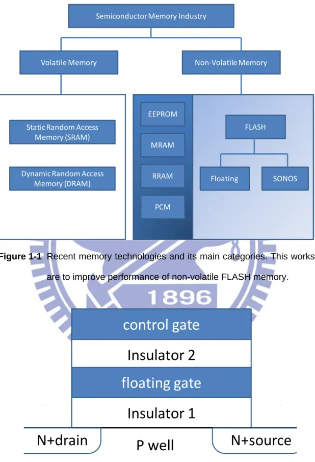
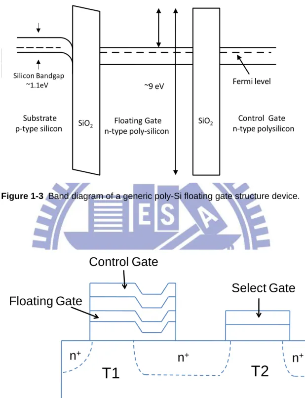
A floating gate (FG) structure memory is expected one of the promising candidates for technology/business nonvolatile memory applications. Figure 1-2 shows the schematic cross section of a generic floating gate device. This floating gate device is MOS-like structure with a polycrystalline Si film inside the gate oxide. Figure 1-3 plots the band diagram of generic floating gate structure. The charges can be forced into or out of the floating gate by biasing the terminal voltage or UV radiation. The threshold voltage changes because the charges are restricted inside the floating gate film by the two SiO2 barriers.
By means of measuring the drain current, storage data can be detected. To date, the stacked-gate FG memory not only replaces magnetic core memory but also create a new era of portable system. In the present day, these devices are widely used in palm top, mobile PC, mp3 audio player, and etc. because they offer the smallest cell size with a very good flexibility [1-1].
In 1967, D. Kahng and S. M. Sze invented the floating gate (FG) nonvolatile memory at Bell Labs [1-2] as shown in Fig. 1-2. The semiconductor between tunneling and blocking oxide had to be thin enough (<5nm) to allow electron tunneling from the channel to the trapping layer to change the threshold voltage.
In 1971’s, the first operating floating gate device was developed by Frohman-Benchowsky at Intel Corporation [1-3], and this cell had no control gate. In this work, the memory cells were programmed by biasing a high-negative voltage and avalanched the drain/substrate junction. This phenomenon creates plasma of highly energetic electrons underneath the gate
3
and the electrons are injected into the floating-gate. The method to provide electrons with escaping energy from trapping layer was UV radiation. However, exposing UV radiation is not an ideal erasing mechanism.
Electrically Erasable Programmable Read only Memory (EEPROM) was developed for accomplishing electrically erasing. Harari [1-4] proposed the FLOTOX (Floating Gate Thin Oxide) which was both programmed and erased by Fowler-Nordheim tunneling. Figure 1-4 is the schematic cross section of EEPROM includes a select transistor and a floating gate transistor. The floating gate transistor is programmed by applying a high voltage to the control gate, and the floating gate voltage increases because of capacitive coupling. With a high electric field, this can cause electron tunneling effect obviously through tunneling oxide into trapping layer. As erasing, the biased drain terminal and grounded control gate can make electrons tunnel through the tunneling oxide from the trapping layer to the channel.
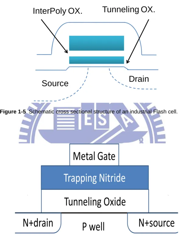
Flash memories are programmed and erased electrically but composed of single transistor cell. Figure 1-5 shows the cross section of an industry-standard Flash cell. This cell structure was presented by INTEL in 1988 and named ETOXTM (EPROM Tunnel Oxide; ETOX is a trademark of INTEL) [1-5]. The cell is not symmetrical. The oxide between the substrate and the floating gate is in the order of 10 nm. Therefore, high biased drain and grounded control gate enhance the electron tunneling current to collect charges of the trapping layer. This operation is very close to the breakdown of the source-substrate junction. Therefore, the source diffusion was realized differently from drain diffusion to avoid high bias.
4
1.2 Concepts of
Semiconductor-Oxide-Nitride-Oxide-Semiconductor (SONOS)
type
Based on floating gate structure, there is another similar structure that is
much more well-known, called Semiconductor-Oxide-Nitride-Oxide-Semiconductor (SONOS) type. The
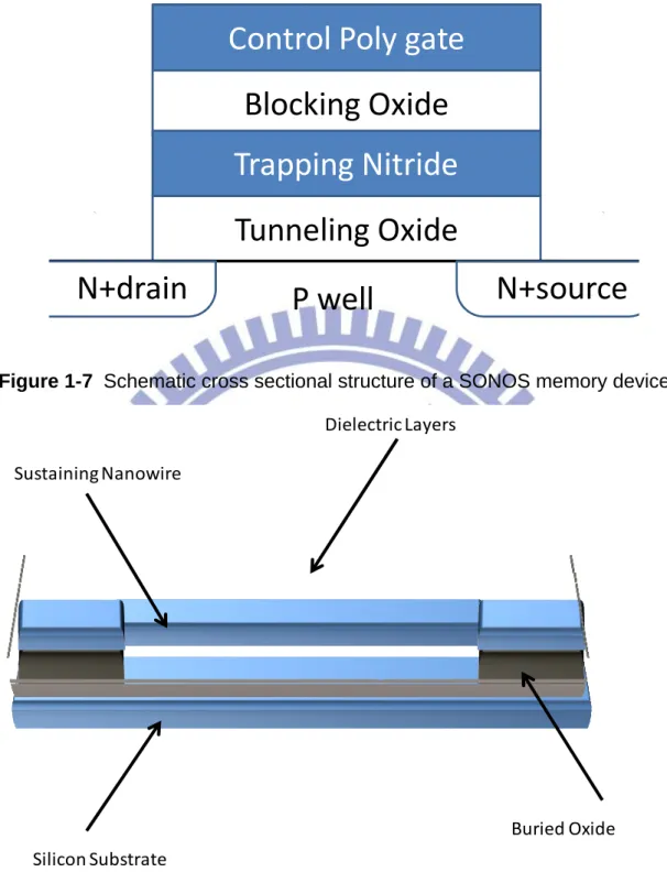
structure is applied widely in non-volatile memory, because a silicon nitride film has sufficient localized and deep energy level traps. Therefore, one leaky path will not cause serious charge loss. MNOS (Metal-Nitride-Oxide-Silicon) was firstly presented in 1967 by Wegener. The schematic cross section of MNOS is shown in Fig. 1-6. A MNOS cell resembles a standard MOS transistor with a nitride/silicon stacked gate oxide film. Charges can be stored in the interface between the silicon and nitride film. But the issue of retention is a main disadvantage of MNOS memories. The read voltage induces an electric field and this will accelerate the escape of stored charges. Therefore, the SNOS (Silicon-Nitride-Oxide-Silicon) structure was proposed to improve the data retention of MNOS memories because the conduction band of silicon is higher than Al metal gate. However, SNOS structure will enhance hole injection form gate electrode. In order to overcome this weakness, a top oxide film is added on the nitride layer to prevent charge exchange between the gate electrode and the nitride film. This SONOS structure is shown in Fig. 1-7. The structure is compatible in silicon process, so the memory device can be fabricated without some issues of processes including film quality or etching. Utilizing this structure is a good choice to research characteristics of non-volatile memory.
5
1.3 Advantages of Gate-All-Around and Dual-Gate
Structures
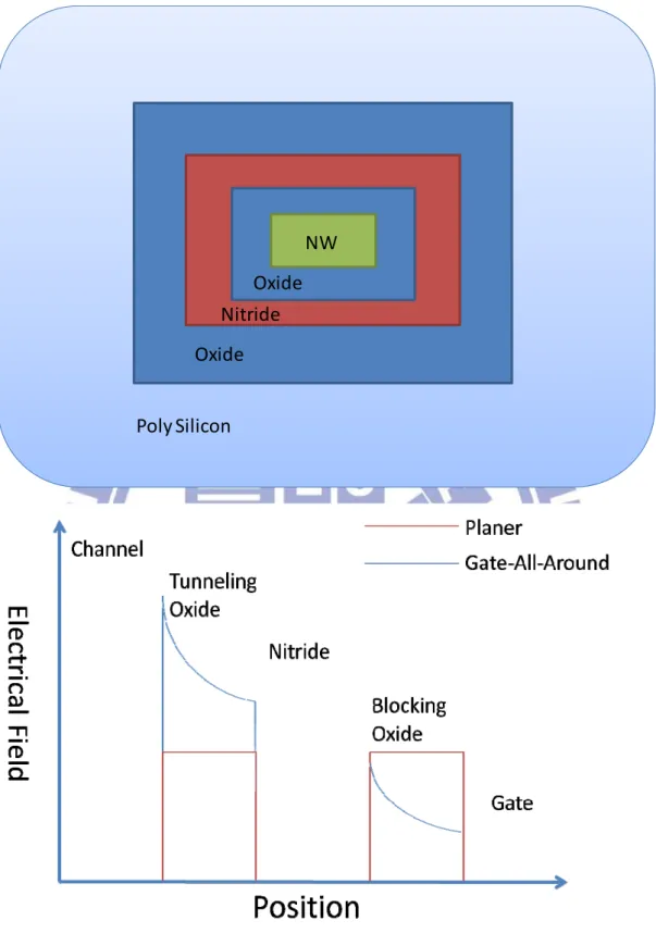
For recent technology trend, feature-size scaling down in CMOS technology has still continued to follow Moore’s law. There are various structures provided to keep the scaling pace. At first, the planer solutions, which is easy to fabricate and design devices, are sufficient to keep scaling including implantation of LDD, lateral no uniformity in channel doping, reduction in junction depth, HALO implants, and etc. However, the planer structures do be natural limitations that are hard to overcome. The major challenges are as follows: (1) degraded the gate electrostatic control of the channel potential leading to short-channel effect – threshold voltage roll-off, large DIBL, and poor sub-threshold swing (SS); (2) increased junction and gate leakage; (3) reduced channel mobility; and (4) increased source/drain (S/D) resistance. They all degrade the performance of devices even scaling down, so the innovative three-dimensional (3D) solutions are proposed intensively. FinFET, Double Gate, Tri-Gate (Pi- or Omega-) and even Gate-All-Around (GAA) are good candidates to create newly semiconductor technologies. Particularly, the gate-all-around structure as shown in figure 1-8 has great potential to increase the gate electrostatic control capability and suppress short-channel effect. The scaling pace starts to jump next generations. The 5-nm gate length device of cylindrical gate-all-around architecture with nanowire channel body has been proposed. For this result, the gate length in these devices can be scaled down with wire diameter without
6
reducing gate dielectric thickness. It is a brilliant future for device design in spite of some issues needed to solve. Furthermore, the gate-all-around structure also can be integrated to non-volatile memory, especially in SONOS-type research, since the gate dielectric can be thicker that generates much more states to store electrons and the electrical field can be enlarged to be application. The performance of non-volatile memory should be better than before. Figure 1-8 and Figure 1-9 exhibit the Gate-All-Around structure with nanowires and its cross sectional views with SONOS structure. Along the corner of nanowires, the distribution of electrical field can be verified, and that is higher than conventional planer structure. For this reason, utilize the Gate-All-Around structure with nanowires, and the performance can be improved significantly.
On the other hand, there are some issues with gate-all-around structure. The most serious one is large electrical field will damage the dielectric material and the reliability will become poor. Therefore, the dual-gate structure has been proposed.[1-6] Its key advantage is reducing lateral electrical field due to the redistribution of electrical field.
1.4 Motivation
In recently technologies proposed for memory devices, they all tried to improve performance of memory, particularly programming and erasing speed and density of memory cell. However, reliability will decrease relatively, and make data storage be unsafe, even errors occurs. That is fatal impact in memory industries, so the better solution is to achieve high performance and
7
sustain enough reliability. First, the gate-all-around structure must release NWs from buried oxide, so some issues of sustaining NWs will be occurred, particularly stress effect. The sustaining NWs will be deformed, so the impact will degrade the performance of GAA devices.
Second, the performance of non-volatile memory must be improved. The programming and erasing speed is concerned depending on the magnitude of electrical field, so the gate-all-around structure device was fabricated. However, the electrical field was enlarged by gate-all-around structure much over that would damage memory cell during operating period. The other concept was proposed, dual-gate structure, which helped release electrical field. Thus, both of structures were combined to fabricate SONOS-type non-volatile memory and achieve high performance and better reliability as expected. Last, the reliability issues of memory must be concerned with high priority. The data should be stored much more safely and keep it read correctly without loss for long time. That is much attracted for consumers. In order to increase reliability, trapping layer engineering has been proposed that not only increases the states to store electrons and also make electrons in the trapping layer much stable. Thus, it is very interesting to integrate with all of these ideas to improve the performance of Gate-All-Around Non-Volatile Memory device. Based on these, we attempt to design the device and fabrication processes according recent semiconductor technologies, and determine the validity of physical meanings to achieve our goals.
8
1.5 Organization of this thesis
In this thesis, to fabricate and characterize high performance of Gate-All-Around Polycrystalline Thin-Film-Transistors Non-Volatile Memory is main topic for research. And then, the topic is divided into three parts to discuss: (a) Formation high quality sustaining nanowires, (b) characteristics of Gate-All-Around Non-Volatile Memory between single gate and dual gate, (c) nanocrystal formation and reliability improvement.
9 Semiconductor Memory Industry Volatile Memory Non‐Volatile Memory Static Random Access Memory (SRAM) Dynamic Random Access Memory (DRAM) EEPROM MRAM RRAM FLASH PCM Floating SONOS
Figure 1-1 Recent memory technologies and its main categories. This works are to improve performance of non-volatile FLASH memory.
control gate
Insulator 1
Insulator 2
floating gate
N+drain
P well
N+source
Figure 1-2 Schematic cross sectional structure of a generic floating gate device.
10 Substrate p‐type silicon Fermi level SiO2 Floating Gate n‐type poly‐silicon SiO2 Control Gate n‐type polysilicon SiO2 ~9 eV Silicon Bandgap ~1.1eV
Figure 1-3 Band diagram of a generic poly-Si floating gate structure device.
n
+n
+n
+Select Gate
Control Gate
Floating Gate
T1
T2
Figure 1-4 Schematic cross sectional structure of EEPROM includes one select transistor (T2) and one floating gate transistor (T1). The drain voltage of floating gate transistors is decided by the select transistors.
11
Tunneling OX.
InterPoly OX.
Source
Drain
Figure 1-5 Schematic cross sectional structure of an industrial Flash cell.
Tunneling Oxide
Metal Gate
Trapping Nitride
N+drain
P well
N+source
Figure 1-6 Schematic cross section of a MNOS structure device. Stacked Nitride/Oxide film is to be gate and store charges.
12
Control Poly gate
Tunneling Oxide
Blocking Oxide
Trapping Nitride
N+drain
P well
N+source
Figure 1-7 Schematic cross sectional structure of a SONOS memory device.
Buried Oxide Silicon Substrate
Sustaining Nanowire
Dielectric Layers
Figure 1-8 Schematic of thin-film transistors based gate-all-around structure with sustaining nanowires.
13 Poly Silicon Oxide Oxide Nitride NW
Figure 1-9 Cross section of nanowires with SONOS structure, and its corner electrical filed distribution.
14
Chapter 2
Basic Mechanisms of Nonvolatile Memory
and its Reliability
2.1 Operation Mechanisms
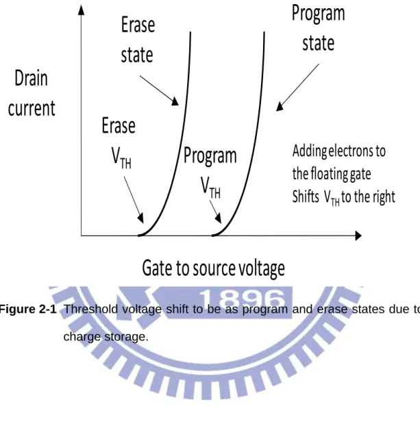
There are three basic operations in a Non-Volatile Memory: read, program, and erase. As mentioned above, one bit data is read by detecting drain current because of different threshold voltages between data “1” and “0”. The difference of threshold voltage is due to trapping layer storage charges. Figure 2-1 indicates threshold voltage shift to be as program and erase states. Therefore, we can control threshold voltage by injecting charges into trapping layer. The operation to collect charges is called program. The operation to remove charges is called erase. Both of them use three basic mechanisms: Fowler-Nordheim (FN) tunneling, channel-hot-carrier (CHC) injection, and band-to-band hot hole (BTBTHH) injection.
Through a high vertical electric field to enhance tunneling effect is the characteristic of FN tunneling. The mechanism of gaining carrier energy by lateral electric and causing impact ionization to cross a silicon oxide barrier is CHC injection. A high reverse bias between gate and drain terminal will build high electric field, and carriers are generated through large conduction and
15
valence band bending in the channel. This phenomenon called BTBT enlarges the carrier density to enhance hot carrier injection effect.
2.1.1 Fowler-Nordheim (FN) Tunneling
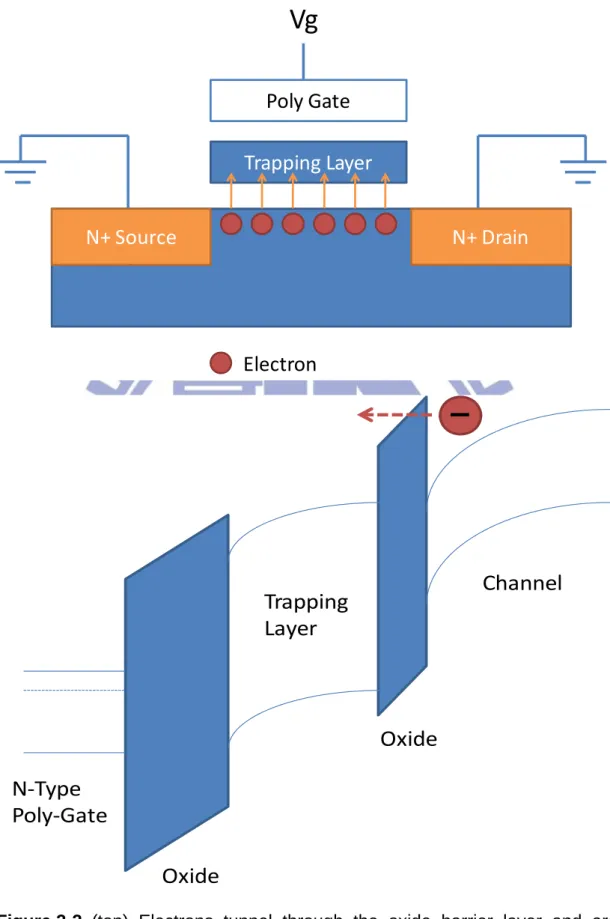
The phenomenon of penetration through the barrier is based on the quantum mechanical nature of the particle. In the classical model, no particle can penetrate the barrier if the kinetic energy of this particle is lower than the barrier height. Therefore, electrons cannot go through silicon oxide barrier layer in a Flash memory if the kinetic energy of electrons is lower than 3.2 eV. However, there is finite possibility to allow penetrating form the substrate to the trapping layer because of wave-particle duality. Direct tunneling current can be controlled by the width of the barrier film and the vertical electric field [2-1].
FN tunneling is a field-assisted carrier tunneling mechanism [2-2]. Figure 2-2 and 2-3 indicates the program and erase operation by FN tunneling, respectively. Free charges of Si-substrate encounter a triangular energy barrier which depends on the applied electric field. The tunneling effect become obviously at a high electric field with the small width of silicon oxide barrier layer. Therefore, charge collecting and removing can be realized in a trapping layer.
2.1.2 Channel-Hot-Carrier (CHC) Injection
16
the free charges in the inversion layer. These accelerated carriers gain kinetic energy as traveling from the source to the drain terminal but loss energy by collision. At the low lateral electric field, dynamic equilibrium between acceleration and collision can be observed. This equilibrium holds until the field strength reaches approximately 100 kV/cm for electrons [2-3]. Under such a high field condition, carriers are no longer in equilibrium, and their kinetic energy begins to increase. At the same time, a gate bias voltage provides an electric field to attract the carriers, and collisions redirect the carriers to the interface. Some of these heated carriers by the high lateral electric field have enough energy to surmount the silicon oxide barrier layer into the trapping layer.
Figure 2-4(top) shows the conduction path and figure 2-4(bottom) shows the band diagram of a CHE operation for a NMOS-type Flash memory. As applying a high drain voltage, the electric field there starts to rise dramatically. Therefore, numerous carriers gain sufficient energy to create impact ionization. This kind of collision breaks down electron-hole pairs and produces the secondary electrons and holes. The majority carriers, electrons, constitute the drain-source current, and the holes travel through the substrate.
2.1.3 Band-To-Band Hot Hole (BTBHH)
Band to band tunneling applied to NVM applications was first proposed in 1989. I.C. Chen demonstrated a high injection efficiency (~1%) mechanism to program EPROM (Erasable Programmable Read Only Memory) [2-4]. Energy
17
band diagram is showed in Fig. 2-5(top). It is well known that electrons are capable of tunneling from the valence band to the conduction band if the band bending is more than Si energy gap. Through applying a high reverse bias across drain and gate terminal, a deep depleted region is build. This depletion region with a high electric field bends the Si-substrate energy band more than 1.1 eV, and band-to-band tunneling effect happens. Through band-to-band tunneling, numerous electron-hole pairs are created. Some of these free carriers gain enough energy by this high electric field to create electron-hole pairs by impact ionization. As shown in Fig. 2-5(bottom), the generated holes redirect to the interface by gate bias voltage or collisions, and some of these holes with enough kinetic energy will cross over the silicon oxide barrier layer. The holes with low kinetic energy cause leakage current flowing into the substrate.
2.2 Reliability
Although the performance and density of Non-Volatile Memory are mainly focuses to design a newly device, there are many issues will also be occurred especially as integrating millions of devices in an array. Because of the data safety for real products, the reliability must be the first priority to consider. To design an excellent reliability with better performance and high density is an important goal for research. However, the performance and reliability should be trade-off to indicate the optimum situation with respect to both of these parameters. There are some benchmarks of reliability to be proposed. The nonvolatilities imply a guarantee of charge retention for ten
18
years, and the cell has to store data after many read/program/erase cycles. Experiments, like cycling and retention, are performed to investigate reliability.
2.2.1 Retention
Non-Volatile Memories are specified to retain stored information for more than ten years. This implies that stored charges in the floating-gate must loss as minimal as possible. In program/erase operation, numerous charges go through thin oxide. This degrades the oxide layer and increases charge loss. The possible reasons of charge loss are: 1) defects in the tunneling oxide; 2) defects in the interpoly dielectric; 3) mobile ion contamination; 4) detrapping of charge from insulating layers surrounding the FG [2-8].
Retention has to be checked by accelerated tests. Therefore, high electric fields and hostile environments, like at high temperature, is used for measuring threshold voltage variation.
2.2.2 Endurance
Today P/E cycles must be guaranteed up to 10,000 times with enough threshold voltage difference. The charge exchange will create traps in the tunneling oxide, and the ability of data retention decreases. The P/E cycles experiment is performed applying constant pulses, and the threshold voltages of programmed state and erased state are measured [2-6], [2-7]. After many program/erase (P/E) cycles, the threshold voltage difference between program
19
state and erase state would decrease due to the tunneling oxide degradation. Therefore, the difficulty of distinguishing current difference increases.
2.2.3 Read Disturbs
During the read operation, the gate and drain terminals of floating-gate memories are biased to cause drain current, and there are still spurious hot carriers surmounting the oxide barrier layer to change the stored data [2-9]. This operation called “soft-programming” is the same with the programming operation, only lower in magnitude. Therefore, frequently repeated read cycles are particularly harmful in the reference cells. For reliability issues, detecting this effect is also very important.
20
Drain
current
Erase
state
Erase
V
TH
Program
V
TH
Program
state
Adding electrons to
the floating gate
Shifts V
THto the right
Gate to source voltage
Figure 2-1 Threshold voltage shift to be as program and erase states due to charge storage.
21
Trapping Layer
Poly Gate
N+ Source
N+ Drain
Vg
Electron
Trapping
Layer
Oxide
Oxide
N‐Type
Poly‐Gate
Channel
Figure 2-2 (top) Electrons tunnel through the oxide barrier layer and are collected in the trapping layer. (bottom) Band diagram of the FN program operation.
22
Poly Gate
N+ Source
N+ Drain
‐Vg
Electron
Trapping
Layer
Oxide
Oxide
N‐Type
Poly‐Gate
Channel
Figure 2-3 (top) Electrons tunnel through the oxide barrier layer and are removed from the trapping layer. (bottom) Band diagram of the FN erase operation.
23
Trapping Layer
Poly Gate
N+ Source
N+ Drain
Electron
Vg
Vd
Trapping Layer Oxide Oxide N‐Type Poly‐Gate ChannelFigure 2-4 (top) Accelerated electrons surmount the oxide barrier layer. (bottom) Band diagram of the Channel-Hot-Electron injection operation.
24
Trapping
Layer
Oxide
Oxide
N‐Type
Poly‐Gate
Channel
Impact ionization
BTB Tunnel
Floating gate
Source
N+ region
Depletion
Substrate
Figure 2-5 (top) Electron-hole pairs created by band-to-band tunneling and impact ionization. (bottom) Some of the generated holes surmount the barrier layer [2-5]
25
Chapter 3
Profile impact of Nanowire Formation with
Sustaining Poly-Silicon
3.1 Formation of Nanowires
The nanowires were fabricated by growing a 400-nm thick thermal silicon dioxide layer on 6 inch silicon wafers initially to be buried oxide. A layer of 50-nm amorphous silicon (a-Si) deposited by low-pressure chemical-vapor deposition (LPCVD) at a temperature at 550 oC, followed by treating solid-phase crystallized (SPC) process at 600oC for 24 hours in nitrogen ambient. The substrate became glass-based wafer. Next, patterning different source/drain length by e-beam lithography was to be active layer, and then dipping into HF to release the nanowires. The source/drain lengths were 2um, 4um, 6um, and 8um respectively. In order to analyze issues of sustaining stress nanowires, oxide(6-nm)/nitride(9-nm)/oxide(12-nm) structure was deposited. Finally, three different tiled-view images of scanning electron microscopy (SEM) were shown. There were top-view, 45-degree, and cross-sectional view to exhibit exact shape of nanowires.
26
In order to form gate-all around structure, the sustaining nanowires must be formed. The buried oxide is removed by HF, and nanowires can be released. However, the strength of nanowires becomes weaker compared with buried oxide existing. The nanowires are deformed by external force easily. A main force is stress due to lattice mismatch. After the oxide/nitride/oxide films are deposited, these films make the nanowires bend exactly. The scanning electron microscopy images show the results as below figures.
Figure 3-1 presents the top-view images. There are 4 different typical source/drain lengths LSD to be discussed: (1) 8-um (2) 6-um (3) 4-um (4) 2-um,
with the same channel width (W = 0.1 um x 10). Figure 3-1a is the longest length of nanowires that shows two different contrasts color at middle and rare of nanowires. Others are normal without any different contrast. That reveals the nanowires with 8-um length may bend. In addition, by measuring width of nanowires in different source/drain lengths, the widths are proportional to 1/LSD,
since E-Beam lithography will scatter in different patterning sizes. That is to be an issue to affect the performance of device. Figure 3-2 presents the 45-degree-view images for 4 source/drain lengths. Figure 3-2a shows a profile of nanowires clearly that are bended exactly after oxide/nitride/oxide films deposited. There are two main regions: (1) Gaussian profile at rare of nanowires; (2) concave profile at middle of nanowires. Other source/drain lengths are all Gaussian profiles. The results demonstrate serious stress occurs, film deposited with high temperature, and various distribution of force applies along nanowires. Figure 3-3 shows bending nanowires are under different stress directions. For 4-um case, the profile of nanowires is Gaussian profile, since there is tensile stress to bend nanowires up; for 8-um case, the
27
source/drain length is too long to sustain the nanowires. At the middle of nanowires, the tensile stress occurs and makes profile become concave profile. Gaussian profile is still maintained in other region. Figure 3-4 exhibits cross sectional view of nanowires with Gaussian profiles for 6-um, 4-um, and 2-um. In these cases, the deformation of nanowires is highly depending on source/drain length. The distance from bottom oxide to the highest nanowires can be measured. Those are 420-nm, 302-nm, and 159-nm for 6-um, 4-um, and 2-um respectively. This result demonstrates the source/drain length decreases, and deformation of nanowires can be also reduced. Thus, that is an important impact for device fabrication. Control gate film will be deposited on nanowires under these various types of stress, and it affects the performance of devices especially for non-volatile memory. The characteristics of memory will discuss later. The summary of different source/drain lengths shows as Table 3-1 as remarks.
28
(a)
(b)
(c)
(d)
Figure 3-1 Top-view scanning electron microcopy images for different source/drain length: (a) 8-um; (b) 6-um; (c) 4-um; (d) 2-um.
29
(a)
(b)
(c)
(d)
Figure 3-2 45-degree-view scanning electron microcopy images for different source/drain length: (a) 8-um; (b) 6-um; (c) 4-um; (d) 2-um.
4 um S/D space
8 um S/D space
S/D Pad
NWs
Stress Direction
30
(a)
(c)
(b)
Figure 3-4 Cross section of various source/drain lengths: (a) 6-um; (b) 4-um; (c) 2-um.
31
S/D Length 8‐um 6‐um 4‐um 2‐um
Profile
Gaussian (side) Concave (mid.)
Gaussian Gaussian Gaussian
Lateral deform High‐ Variation Medium‐ Variation Low‐ Variation Non‐ Variation Vertical deform* N/A 420 nm 302 nm 159 nm
Table 3-1 Summary with different source/drain lengths contains profile and deformation.
Ox
Ox
Act
Act
The distance
defines as *.
32
Chapter 4
Characteristics of Non-Volatile Memory
with Dual Gate-All-Around structure
4.1 Device Fabrication
The gate-all-around memory devices were fabricated by growing a 400-nm thick thermal silicon dioxide layer on 6 inch silicon wafers initially to perform like the glass substrate. A layer of 50-nm amorphous silicon (a-Si) deposited by low-pressure chemical-vapor deposition (LPCVD) at a temperature at 550 oC, followed by treating solid-phase crystallized (SPC) process at 600oC for 24 hours in nitrogen ambient. For nanowires (NWs) patterning, active layer was defined by electron beam (e-beam), and then dipped in DHF to release NWs. The thickness of tunneling oxide, nitride, and blocking oxide (ONO structure) were 6-nm, 9-nm, and 12-nm respectively grown by LPCVD. Among them, the trapping layer was formed by Si3N4 (3nm) /
a-Si (3nm) / Si3N4 (3nm) as a quantum well. Three-dimension schematic of all
dual gate-all-around structure can be shown as figure 4-1. Finally, the N+ doped poly-silicon was deposited as dual gate electrode, that could be activation without annealing process, and patterned by e-beam and RIE. Self-align phosphorous implantation was performed and source/drain regions were activation by rapid thermal anneal (RTA) process. The sequent
33
passivation and metallization were standard process with recent technologies, which 200-nm oxide layer with PECVD TEOS and 300-nm Al-Si-Cu metal layer with Physical Vapor Deposition (PVD) respectively.
4.2 Characteristics Analysis
Figure 4-2 presents top-view of a dual-gate structure nanowires non-volatile memory device, and scanning electron microscopy image confirms channel length is about 2.5 um for each gate (G1 and G2). In addition, the spacing between G1 and G2 is about 1.5 um. Figure 4-3(left) shows the cross-sectional the nanowires channel along of AA’ line transmission electron microscopy image of each nanowire. The poly-Si nanowire channel was surrounded by Oxide/Nitride/Oxide structure and N+ poly definitely, that the physical width is 120 nm and the height is 40 nm of rectangular-shape channel. Figure 4-3(right) is a high-resolution (HR) transmission image that indicates practical ONO structure including the engineered charge trapping layer with nanocrystals which dimensions are about 5 nm; therefore, nanocrystals can be formed by a suitable anneal recipe in Nitride/a-Si/Nitride structure certainly.
Multi-channel devices have excellent characteristics in thin-film-transistor [4-1]. For non-volatile memory application, various devices have been fabricated as table 4-1. Totally, there are four different channel numbers to analysis: (1) S1; (2) M3; (3) M5; (4) M10. Figure 4-4 shows Id-Vg transfer characteristic after programming with positive bias 12 V for 1 ms. The memory windows of all devices increase depending on more channel numbers as
34
shown in Figure 4-5, since the channel edge and corner effect enhance electrical field to increase programming efficiency. However, even multi-channel devices have an advantage of large memory windows, but leakage current also increases due to electrical stress in dielectric. For long period operation, reliability issues will occur easily. Thus, the channel numbers must be modified. That leakage current can’t increase too much and enough memory windows exist. These parameters are to be optimized.
Figure 4-6 shows Id-Vg characteristics of Dual Gate-all-around (DGAA) (Lg = 2.5 × 2 um) and Single Gate-all-around (SGAA) devices (Lg = 5.0 × 1 um)
in initial and programmed states. Both cells have a few threshold voltage differences with positive pulse 12 V for 1 ms, and the leakage current of DGAA is still suppressed obviously after programming. The channel of DGAA structure is under compressive stress, and the SGAA is at tensile stress. At the tensile region, the higher leakage current of SGAA structure appears, since the dielectric induces more damages than compressive stress. Hence, the type of stain alters dielectric properties that shown in characteristics of the devices. Figure 4-7 shows program and erase (P/E) characteristics, which exhibits high performance in program and erase operations. Applied positive programming voltages are from 10 V and 14 V, and the negative erasing voltages are also the same level. In low voltage P/E operation, sustained memory window is large enough to distinguish program and erase level. The electrical field will be enhanced by corner effect, increasing the P/E efficiency through FN tunneling mechanism. On the other hand, the SGAA structure fails in specific operation condition of DGAA. The concave-profile isn’t appropriate for film deposition, and it causes the dielectric strength become weaker than Gaussian-profile.
35
The result explains SGAA with weaker dielectric breakdown easily. Figure 4-8 shows retention characteristics, and the memory window of DGAA is 83% maintenance after ten-year; nevertheless, the memory window of SGAA is only 54%. These distinct effects from structure differences due to varied dielectric strength. The electrons loss easily from the charge trapping layer in SGAA structure since the dielectric with tensile stress is difficult to maintain electrons compared with compressive stress. Figure 4-9 indicates endurance characteristics with DGAA and SGAA. The memory window of DGAA is 74% after 104 cycles, but SGAA structure fails under only 100 times cycles and smaller memory window. As P/E discussed, the tensile stress induces weaker dielectric strength, and the SGAA devices are easy to breakdown after a few numbers of P/E cycles. All these results demonstrate the different strained NWs profiles lead to alter characteristics of devices. The deformed NWs with compressive stress perform a better dielectric deposition and properties to improve the performance of NVM, especially DGAA structure shown better characteristics.
For dual gate-all-around non-volatile memory devices, there are an amount of advantages compared with single-gate structure. The following discussions are just focus on its performance. Figure 4-10 shows the P/E characteristics with various pulse widths at different gate bias conditions. A large memory window of 3 V at a gate bias of 14 V for 100 us can be achieved for dual-gate GAA NWs NVM, so this device can be low power and high speed application. Figure 4-11 indicates excellent P/E speed of various channel length. The dual-gate device can be scaling down further to achieve high-density applications with high performance. Figure 4-12 presents the read
36
disturb of the dual GAA NVM device with two read conditions. For gate voltage 1.8 V and drain voltage 0.5 V, the Vth appears stable in programmed and
erased states. For more strict condition, drain voltage increasing to 3.0 V, the Vth still maintains stable without voltage shift. The reliability of DGAA is also
improved such as retention and endurance. This is contributed by the charge trapping layer engineering due to charge confinement in the deep quantum well. There are additional states in trapping layer to store charge, and it is hard to loss in equilibrium condition. Consequently, this type of non-volatile memory has much attractive for future applications.
37
D
S
G
Figure 4-1 The three-dimension schematic of a dual gate-all-around non-volatile memory device and its process flows.
38
A’
A
Figure 4-2 (left) Top view of a dual-gate nanowires thin-film-transistor non-volatile memory. (right) Scanning electron microscopy image of top view.
Figure 4-3 (left) Transmission electron microscopy cross section image corresponding to figure 4-3(left), in the AA’ direction. (right) High-resolution transmission electron microscopy image.
39 Device Name Gate Length Channel Number Each Width Effective Width S1 5 um 1 100 nm 1.69 um M3 5 um 3 320 nm 1.42 um M5 5 um 5 0.5 um 1.30 um M10 5 um 10 1.0 um 1.00 um
Table 4-1 Various non-volatile memory devices with different channel numbers and its scale dimension.
Gate Voltage (V)
-2 -1 0 1 2 3 4 5Drain Cur
rent (A)
10-13 10-12 10-11 10-10 10-9 10-8 10-7 10-6 10-5 Initial State S1 M2 M5 M10Figure 4-4 Ids-Vgs transfer characteristic of different channel numbers after
40 S1 M3 M5 M10
Δ
V
th
0.0 0.2 0.4 0.6 0.8 1.0 1.2 1.4 1.6 1.8 2.0Figure 4-5 Threshold voltage shift in different channel numbers after programming. Gate Voltage (V) -2 -1 0 1 2 3 4 5 Dr ain Cur ren t (A) 10-13 10-12 10-11 10-10 10-9 10-8 10-7 10-6 10-5
DGAA (2.5 x 2 um): Initial DGAA (2.5 x 2 um): Program, Vp=12 V, tp=1 ms SGAA (5.0 x 1 um): Initial state SGAA (5.0 x 1 um):
Program, Vp=12 V, tp=1 ms
Figure 4-6 Ids-Vgs transfer characteristics of dual-gate GAA device in initial
41
Time (sec)
10-7 10-6 10-5 10-4 10-3 10-2 10-1 100Δ
V
th
(V)
-4 -2 0 2 4 SGAA ( Lg=5.0 x 1 um ) Vg = 10 V SGAA ( Lg=5.0 x 1 um ) Vg = -10 V SGAA ( Lg=5.0 x 1 um ) Vg = 14 V SGAA ( Lg=5.0 x 1 um ) Vg = -14 V DGAA ( Lg=2.5 x 2 um ) Vg = 10 V DGAA ( Lg=2.5 x 2 um ) Vg = -10 V DGAA ( Lg=2.5 x 2 um ) Vg = 14 V DGAA ( Lg=2.5 x 2 um ) Vg = -14 VFigure 4-7 P/E characteristics under the various FN bias conditions. The cross marks show the failure operation conditions.
Time (sec)
100 101 102 103 104 105 106 107 108 109T
h
re
shol
d Voltage (V)
0.5 1.0 1.5 2.0 2.5 3.0 3.5DGAA Programmed State DGAA Erased State SGAA Programmed State SGAA Erased State
10 years
83%
Figure 4-8 Retention characteristics sustain 83% of memory window for 10-year period with dual-gate structure, and the differences of retention are obviously compared with single-gate.
42 Cycles 100 101 102 103 104 Tr es hol d V o lt age ( V ) 0 1 2 3 4 5
DGAA Program; Vgs = 14 V 0.01 msec DGAA Erase; Vgs = -18 V 0.5 msec
SGAA Program; Vgs = 13 V 0.01 msec SGAA Erase; Vgs = -15 V 1.0 msec
BKD
Figure 4-9 Endurance characteristics sustain 76% of memory window over 104 with dual-gate structure, and it compared with single-gate that failed easily.
Time (sec)
10-7 10-6 10-5 10-4 10-3 10-2 10-1 100Δ
V
th
(V)
-4 -2 0 2 4 Vgs = 8 V Vgs = 12 V Vgs = 14 V Vgs = -9 V Vgs = -11 V Vgs = -14 VFigure 4-10 P/E characteristics under the various FN bias conditions with dual gate-all-around structure.
43
Time (Sec) 10-7 10-6 10-5 10-4 10-3 10-2 10-1 ΔV th (V ) -2 -1 0 1 2
3 Programmed State L = 5.0 x 2 umProgrammed State L = 2.5 x 2 um Programmed State L = 1.0 x 2 um Erased State L = 5.0 x 2 um Erased State L = 2.5 x 2 um Erased State L = 1.0 x 2 um Vgs = 12 V Vgs = -12 V
Figure 4-11P/E characteristics of dual GAA NVMs with the same channel width but various channels. The shorter channel length still sustains P/E speed.
Time (Sec)
100 101 102 103T
h
re
shold Voltage (
V
)
0.0 0.5 1.0 1.5 2.0 2.5 3.0 Erased State Vgs = 1.8 V Vds = 0.5 V Programmed State Vgs = 1.8V Vds = 0.5 V Erased State Vgs = 1.8 V Vds = 3.0 V Programmed State Vgs = 1.8 V Vds = 3.0 VFigure 4-12 Read disturb characteristics of dual GAA NVM with various drain voltage. It is stable in read operation period.
44
Time (sec)
100 101 102 103 104 105 106 107 108 109T
h
reshold Voltage (
V
)
0.5 1.0 1.5 2.0 2.5 3.0 3.5 Programmed State Erased State 10 years 83%Figure 4-13 Good retention is contributed by nanocrystal trapping layer due to quantum confinement.
45 Oxide Oxide N‐Type Poly‐Gate Channel NC
Oxide
Oxide
N‐Type
Poly‐Gate
Channel
NCFigure 4-14 Band diagram with nanocrystal in trapping layer (top) programming (bot) store.
46
Chapter 5
Conclusion
In this work, multi-channel gate-all-around non-volatile memory devices have been proposed. The performance of device is improved by Multi-channel structure, and also the strength of nanowires without buried oxide layer is reduced seriously; nevertheless, gate-all-around structure must construct on these stylish nanowires. The profile of nanowires is highly depending on source/drain length due to stress. Decreasing source/drain length is an important parameter to keep nanowires be Gaussian profile, and that is compatible for gate-all-around device fabrication.
On the other hand, the dual gate-all-around (DGAA) structure device is a good candidate for non-volatile memory application compared with single gate-all-around (SGAA), particularly, its high reliability and performance are observed. And depending on types of strained nanowires between SGAA and DGAA, the profiles of nanowires are crucial phenomenon on physical characteristics. The performance enhanced relate to compressive stress DGAA device with strong dielectric strength. Moreover, the retention and endurance only degrade 17% and 26% compared with that of failed tensile stress SGAA devices. Hence, the profiles of nanowires poly-S impact the characteristics of memories intensely. In addition, the design of device can be improved scaling down by advanced lithography, and the performance of
47
non-volatile memory device is also improved. Simultaneously, the stress effect on the nanowires is reduced, and the complexity of processes is also lower. This investigation would examine the nanowires poly-Si thin-film-transistor memories on future active matrix liquid crystal display system-on-panel and three-dimension stacked high-density applications.
48
References
Chapter 1
[1-1]. Roberto Bez, Emilio Camerlenghi, Alberto Modelli, and Angelo Visconti “Introduction to Flash Memory,” Proc. IEEE 91, 489–502, 2003.
[1-2]. D. Kahng and S. M. Sze, Bell Syst. Tech. J. 46, 1288, 1967.
[1-3]. Kahng D. and Sze S.M., “A floating gate and its application to memory devices”. Bell syst. Tech. J.,46, pp.1288, 1967.
[1-4]. Harai E., Schmitz L., Troutman B., and Wang S., “A 256 bit nonvolatile static RAM”. IEEE ISSCC TECH. Dig., pp.108, 1978.
[1-5]. Kynett V.N., Baker A., Frandrich M., Hoekstra G.,Jungroth O., Kreifels J., and Wells S., “ An in-system reprogrammable 256K CMOS Flash memory”,
ISSCC Tec. Dig., pp.132, 1988.
[1-6]. Yung-Chun Wu, Ting-Chang Chang, Po-Tsun Liu, Cheng-Wei Chou Yuan-Chun Wu, Hun-Hao Tu, and Chun-Yen Chang, “TNANO High-Performance Metal-Induced Lateral-Crystallization Polysilicon Thin-Film Transistors With Multiple Nanowire Channels and Multiple Gates,” IEDM Tech. Dig. 2006.
[1-7]. Navab Singh, Kavitha D. Buddharaju, S. K. Manhas, A. Agarwal, Subhash C. Rustagi, G. Q. Lo, N. Balasubramanian, and Dim-Lee Kwong, “Si, SiGe Nanowire Devices by Top-Down Technology and Their Applications,” IEEE Transactions on Electron Devices, Vol. 55, No. 11, pp. 3107, 2008. [1-8]. Po-Chun Huang, Lu-An Chen, and Jeng-Tzong Sheu, “Electric-Field Enhancement of a Gate-All-Around Nanowire Thin-Film Transistor Memory,” IEEE Electron Device Letters, Vol. 31, No. 3, pp.216, 2010.
49
[1-9]. Sung Dae Suk, Kyoung Hwan Yeo, Keun Hwi Cho, Ming Li, Yun young Yeoh, Ki-Ha Hong, Sung-Han Kim, Young-Ho Koh, Sunggon Jung, Won Jun Jang, Dong-Won Kim Donggun Park, and Byung-Il Ryu, “Gate-all-around Twin Silicon nanowire SONOS Memory,” Sym. VLSI Technology, pp. 142, 2007. [1-10]. J. Fu, K. D. Buddharaju, S. H. G. Teo, Chunxiang Zhu, M. B. Yu, N. Singh, G. Q. Lo, N. Balasubramanian, and D. L. Kwong, “Trap Layer Engineered Gate-All-Around Vertically Stacked Twin Si-Nanowire Nonvolatile Memory,” IEDM Tech. Dig., pp. 79, 2007.
[1-11]. J. Fu, N. Singh, K. D. Buddharaju, S. H. G. Teo, C. Shen, Y. Jiang, C. X. Zhu, M. B. Yu, G. Q. Lo, N. Balasubramanian, D. L. Kwong, E. Gnani, and G. Baccarani, “Si-Nanowire Based Gate-All-Around Nonvolatile SONOS Memory Cell,” IEEE Electron Device Letters, Vol. 29, No. 5, pp. 518, 2008.
[1-12]. Jeong-Dong CHOE, Se-Hoon Lee, Jong Jin Lee, Eun Suk Cho, Youngjoon Ahn, Byoung Yong Choi, Suk Kang Sung, Jintae No, Ilsub Chung, Kyucharn Park, and Donggun Park, “Fin-Type Field-Effect Transistor NAND Flash with Nitride/Silicon/Nanocrystal/Nitride Hybrid Trap Layer,” J. Journal of Applied Physics, Vol. 46, No. 4B, pp. 2197, 2007.
[1-13]. Shih-Ching Chen et al., “Nonvolatile polycrystalline silicon thin-film-transistor memory with oxide/nitride/oxide stack gate dielectrics and nanowire channels,” Applied Physics Letters 90, 122111, 2007.
[1-14]. Tsung-Yu Chiang, Tien-Sheng Chao, Yi-Hong Wu, and Wen-Luh Yang, “High-Program/Erase-Speed SONOS With In Situ Silicon Nanocrystals,” IEEE Electron Device Letters, Vol. 29, No. 10, pp. 1148, 2008.
Chapter 2
50
[2-2]. M. Lenzlinger, “Fowler-Mordheim Tunneling in thermal grown SiO2”, Appl.
Phys. Lett., Vol. 40, pp. 278-283, 1969.
[2-3]. P. E. Cottrell, R. R. Troutman, and T. H. Ning, “Hot-electron emission in n-channel
IGFETs,” IEEE J. Solid-State Circuits, Vol. 14, pp. 442, 1979.
[2-4]. I. C. Chen, C. Kaya and J. Paterson, “Band-to-band tunneling induced substrate
hot-electron (BBISHE) injection: A new programming mechanism for nonvolatile
memory devices,” IEDM, pp.263, 1989.
[2-5]. K. Tamer San, Cetin Kaya, and T. P. Ma, “Effects of Erase Source Bias On Flash EPROM Device Reliability”, Transactions on Electron Devices, Vol. 42, pp.150, 1995.
[2-6]. P. Cappelletti, R. Bez, D. Cantarelli, and L. Fratin, “Failure mechanisms of Flash
cell in program/erase cycling,” IEDM Tech. Dig., pp. 291–294, 1994.
[2-7]. Roberto Bez, Emilic Camerlenghi, Alberto Modelli, and Angelo Visconti, “Introduction to Flash Memory,” Proc. IEEE, Vol. 91, pp. 489-502, 2003.
[2-8]. Roberto Bez, Emilio Camerlenghi, Alberto Modelli, and Angelo Viscontio, “Introduction to Flash memory,” Proceedings of the IEEE, vol. 91, pp.489,2003.
[2-9]. Van Houdt J.F., Wellekens D., Ravazzi L., and Sangiorigi E., “Soft-programming in scaled flash memory cells,” H.C. de Graaf and H.V. Kranemburg (Eds.), Proc. ESSDERC 95, The Hague (The Netherlands), pp. 549.
51
Chapter 3
[3-1]. Jin-Woo Han, Dong-Il Moon, and Yang-Kyu Choi, “High Aspect Ratio Silicon Nanowire for Stiction Immune Gate-All-Around MOSFETs,” IEEE Electron Device Letters, pp. 864, 2009.
[3-2]. L. De Michielis, K. E. Moselund, D. Bouvet, P. Dobrosz, S. Olsen, A. O’Neill, L. Lattanzio, M. Najmzadeh, L. Selmi. And A. M. Ionescu,
“Optimization of the Channel Lateral Strain Profile for Improved Performance of Multi-Gate MOSFETs,” VLSI, pp. 119, 2009.
Chapter 4
[4-1]. Yung-Chun Wu, Chun-Yen Chang, Ting-Chang Chang, Po-Tsun Liu, Chi-Shen Chen, Chun-Hao Tu, Hsiao-Wen Zan, Ya-Hsiang Tai, and Simon Min Sze, “High Performance and High Reliability Polysilicon Thin-Film Transistors with Multiple Nano-Wire Channels,” IEDM, pp. 777, 2004.