700 IEEE ELECTRON DEVICE LETTERS, VOL. 28, NO. 8, AUGUST 2007
Thickness Scaling and Reliability Comparison for
the Inter-Poly High-
κ
Dielectrics
Yung-Yu Chen and Chao-Hsin Chien
Abstract—In this letter, the inter-poly dielectric (IPD) thick-ness, scaling, and reliability characteristics of Al2O3 and HfO2
IPDs are studied, which are then compared with conventional oxide/nitride/oxide (ONO) IPD. Regardless of deposition tools, drastic leakage current reduction and reliability improvement have been demonstrated by replacing ONO IPD with high-permittivity (high-κ) IPDs, which is suitable for mass production applications in the future. Moreover, metal–organic chemical va-por deposition (MOCVD) can be used to further promote dielec-tric reliability when compared to reactive-sputtering deposition. By using the MOCVD, the charge-to-breakdown (QBD) can be
significantly improved, in addition to enhanced breakdown voltage and effective breakdown field. Our results clearly demonstrate that high-κ IPD, particularly deposited by MOCVD, possesses great potential for next-generation stacked-gate Flash memories.
Index Terms—High-κ dielectric, inter-poly dielectric (IPD), metal–organic chemical vapor deposition (MOCVD).
I. INTRODUCTION
R
ECENTLY, the Flash memory market has shown ex-ponential increases, particularly in areas of mass stor-age applications. In the coming decade, we will be required to provide Flash technologies that are compatible with the read/write speed of embedded dynamic random access memory and high nonvolatility [1]. In order to meet the requirement, next-generation Flash memories must possess not only reduced leakage current through inter-poly dielectric (IPD) and tunnel oxide but must also feature improved breakdown field and QBD of the dielectrics in order to suppress charge loss. However, it is not sufficient to meet the stringent insulating requirement of the IPD while applying thermal or chemical-vapor-deposited oxynitride technologies due to the unavoidable leakage current [2]. In order to accomplish this without a tradeoff between low-power and high-speed operations, stacked-gate Flash memory with high gate coupling ratio should be achieved by increasing the floating gate capacitance [3]–[7].There are three different approaches that can be used to increase the gate coupling ratio. The first method is to decrease the IPD thickness. Oxide/nitride/oxide (ONO) multilayered films have been extensively researched and frequently used
Manuscript received April 16, 2007; revised May 22, 2007. The review of this letter was arranged by Editor C.-P. Chang.
Y.-Y. Chen is with the Department of Electronic Engineering, Lunghwa University of Science and Technology, Taoyuan 333, Taiwan, R.O.C. (e-mail: [email protected]).
C.-H. Chien is with the Institute of Electronics, National Chiao-Tung University, Hsinchu 300, Taiwan, R.O.C.
Digital Object Identifier 10.1109/LED.2007.901590
as the dielectric layer in Flash memory devices and other applications [3]. However, decreasing the thickness of the IPD to increase the coupling ratio may cause serious leakage and reliability problems that are detrimental to the charge storage of Flash memories [4]. The second method involves increasing the area of the IPD capacitor. High capacitive-coupling ratio cell [5], 3-D IPD, and hemisphere grain [6] have all been proposed to effectively increase the capacitance area and to lower the control gate bias. Although the coupling ratio can be dramat-ically improved from the aforementioned cell structures, their inclusion into the fabrication process would require several additional process steps due to the complex structures involved, making the process difficult to control effectively. The final approach is to increase the dielectric constant (κ) of the IPD materials [7]. It is straightforward and effective to incorporate alternative high-permittivity (high-κ) materials on nonvolatile memories to replace ONO IPD for increasing floating gate capacitance and suppression of charge loss without increasing cell area and complexity of fabrication.
Previously, we had presented the effects of surface ammonia (NH3) nitridation and post-deposition annealing (PDA) temper-ature on reactive-sputtered (RS) aluminum oxide (Al2O3) IPD characteristics [8]. However, even after process optimization, the QBD of RS-Al2O3 IPD is relatively low. In this letter, thickness scaling and the reliability characteristics of inter-poly Al2O3and hafnium oxide (HfO2) dielectrics are compared with the ONO IPD. Drastic leakage current reduction and reliability improvement can be demonstrated by replacing the ONO IPD with high-κ IPDs, which are suitable for mass production applications in the future.
II. EXPERIMENTAL
The n+-polysilicon/IPD/n+-polysilicon capacitors were fab-ricated on 6-in p-type (100)-oriented silicon wafers. A 200-nm bottom polysilicon film (Poly-I) was deposited on the buffer ox-ide by low-pressure chemical vapor deposition (LPCVD) sys-tem using SiH4gas at 620◦C and subsequently implanted with phosphorous at 5× 15 cm−2, 20 keV. It was then activated with rapid thermal annealing (RTA) at 950◦C for 30 s. Prior to the deposition of the IPD, the Poly-I was cleaned by conventional RCA cleaning and sequentially etched in diluted hydrofluoric acid for the removal of particles and native oxides. The samples were then subjected to NH3nitridation in the LPCVD furnace at 800◦C for 1 h to suppress interfacial layer growth and improve the dielectric properties [8]. Al2O3 and HfO2 IPDs were de-posited either by RS in an Ar/O2ambient at room temperature 0741-3106/$25.00 © 2007 IEEE
CHEN AND CHIEN: THICKNESS SCALING AND RELIABILITY COMPARISON 701
Fig. 1. Current density at low electric field (3 MV/cm) as a function of EOT for various IPDs.
or by metal–organic chemical vapor deposition (MOCVD) with oxygen gas. PDA of Al2O3and HfO2IPDs were carried out by RTA at 900◦C and 800◦C, respectively, for 30 s. Conventional ONO IPD was used for references. The ONO IPD consists of a 1.5–2-nm thermally grown bottom oxide on the Poly-I at 850 ◦C in an O2/N2 environment, a 4–9-nm LPCVD nitride layer is then deposited on top at 700 ◦C using SiH2Cl2 and NH3 gases, and lastly, a 1–1.5-nm top oxide was formed by wet oxidation of the nitride layer at 950 ◦C in an O2/H2 ambient. Subsequently, a 200-nm top polysilicon layer (Poly-II) was deposited by LPCVD and implanted with phosphorous at 5× 15 cm−2, 20 keV. Dopants were then activated with RTA at 950 ◦C for 30 s. After gate stacks were patterned, 500-nm TEOS oxide passivation and Al metallization were defined. Equivalent oxide thickness (EOT) was obtained from the high-frequency (100 kHz) capacitance–voltage measurement using a Hewlett-Packard (HP) 4284 LCR meter. The electrical prop-erties and reliability characteristics of the inter-poly capacitors were measured using an HP4156 C semiconductor parameter analyzer.
III. RESULTS ANDDISCUSSIONS
Fig. 1 plots the leakage current density at relatively low electric field (3 MV/cm) for various high-κ IPD candidates. The leakage current density is shown to be increasing as the EOT of the IPD is scaling down. Compared to the ONO IPD, high-κ IPDs can reduce the leakage current density greater than one order of magnitude in both polarities at the same EOT. Since leakage path elimination between the Poly-I and Poly-II is a critical issue in the design criteria of the stacked-gate Flash memories to sustain charge storage, it is expected that Flash memories with high-κ IPDs can significantly suppress charge loss than ONO IPD.
Breakdown voltage (BV) comparisons between the high-κ IPDs and ONO IPD are shown in Fig. 2. As the EOT is scaled down, the BV decreases due to the reduced critical trapping density for dielectric breakdown [9]. RS-Al2O3 IPD can provide BV increment of greater than 1 V when compared with the ONO IPD in both polarities, although the
improve-Fig. 2. BV comparison for RS-deposited, MOCVD-deposited high-κ IPDs and ONO IPD.
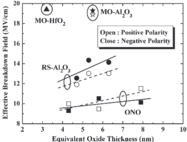
Fig. 3. Effective breakdown field as a function of EOT for RS-deposited, MOCVD-deposited high-κ IPDs and ONO IPD.
ment seems to diminish for EOT less than 5-nm. Fortunately, the MO-Al2O3 IPD exhibits a BV of larger than 10 V, which is nearly twice than that of the ONO IPD. By adopting the MO-HfO2, the BV can be maintained at greater than 6 V as the EOT = 3.3-nm regime.
After eliminating the thickness dependence, the resulting effective breakdown electric field ( BEeff), which is defined as the ratio of BV to EOT, of high-κ IPDs is still higher than the ONO IPD, as presented in Fig. 3. BEeff is extended to greater than 2 and 8 MV/cm for RS- and MO-Al2O3IPDs, respectively. Both MO-Al2O3and HfO2IPD can withstand breakdown fields as high as 19 MV/cm, which is enough to be applied for the next-generation Flash memory.
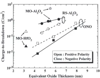
In terms of dielectric reliability, the high-κ IPDs also exhibit superior QBD than the ONO IPD, as shown in Fig. 4. Our results indicate that QBD-value of IPDs is strongly dependent on the dielectric thickness. From the percolation model [9], the critical electron trap density is strongly dependent on the thickness and inherent physical properties of the dielectric. Therefore, thicker IPDs exhibit higher BV and QBD mean value, contributing to the bulk-dominant dielectric breakdown
702 IEEE ELECTRON DEVICE LETTERS, VOL. 28, NO. 8, AUGUST 2007
Fig. 4. Comparison of 63% failure rate QBD between RS-deposited,
MOCVD-deposited high-κ IPDs and ONO IPD.
in both polarities. RS-Al2O3 IPD reveals a near one order of magnitude QBD improvement than the ONO IPD in both polarities.
On the other hand, despite the fact that the RS-Al2O3 IPD can tolerate higher QBDthan the ONO IPD, the maximum QBD observed is only∼1 C/cm2, which may present a major limita-tion for the RS-Al2O3IPD to replace conventional IPDs. Insuf-ficient QBD becomes more severe as the EOT is scaled down due to the bulk-dominant dielectric breakdown, as predicted by the percolation model [9]. Fortunately, QBD can be drastically improved by the MOCVD instrument. The 63% failure QBDof MO-Al2O3IPD is about 5.5 C/cm2in positive polarity, which is a near one order of magnitude improvement compared with the RS-Al2O3 IPD in the same polarity. Nevertheless, negli-gible QBD improvement is observed for negative polarity. For MO-HfO2IPD, the calculated QBDis relatively poor partially from a thinner EOT than Al2O3IPD.
Although the real mechanisms for dielectric characteristic promotion of MOCVD-deposited IPDs are not clear as of yet, one possible explanation is speculated to be from the decreased defect density and uniform thickness of MOCVD-deposited dielectrics. Consequently, the EOT of IPDs can be further scaled down to 3.3 and 4.6-nm by HfO2 and Al2O3 IPDs, respectively, without significant degradation of dielectric characteristics.
IV. CONCLUSION
In the comparison of dielectric characteristics, including the leakage current density, BV, effective breakdown field, and
QBD between RS- or MOCVD-deposited high-κ IPDs and conventional ONO IPD, the results clearly indicate that high-κ IPDs, regardless of deposition tools, exhibit high potential as a replacement to conventional ONO IPD. Moreover, IPD reliability is also shown to be strongly dependent on deposi-tion instruments; the MOCVD-deposited IPDs reveal superior reliability improvements than the RS-deposited dielectrics. The
QBDcan be significantly improved, in addition to the enhanced BV and effective breakdown field through the use of MOCVD instead of RS. Our results clearly demonstrate that both MO-Al2O3 and MO-HfO2 IPDs possess high potential for next-generation stacked-gate Flash memories.
REFERENCES
[1] The International Technology Roadmap for Semiconductors, 2003 ed., Semicond. Ind. Assoc., San Jose, CA.
[2] S. Mori, E. Sakagami, H. Araki, Y. Kaneko, K. Narita, Y. Ohshima, N. Arai, and K. Yoshikawa, “ONO inter-poly dielectric scaling for non-volatile memory applications,” IEEE Trans. Electron Devices, vol. 38, no. 2, pp. 386–391, Feb. 1991.
[3] N. Matsuo and A. Sasaki, “Electrical characteristics of oxide-nitride-oxide films formed on tunnel-structured stacked capacitors,” IEEE Trans.
Electron Devices, vol. 42, no. 7, pp. 1340–1343, Jul. 1995.
[4] Y. Yamaguchi, E. Sakagami, N. Arai, M. Sato, E. Kamiya, K. Yoshikawa, H. Meguro, H. Tsunoda, and S. Mori, “ONO interpoly dielectric scaling limit for non-volatile memory devices,” in VLSI Symp. Tech. Dig., 1993, pp. 85–86.
[5] J. D. Choi, J. H. Lee, W. H. Lee, K. S. Shin, Y. S. Yim, J. D. Lee, Y. C. Shin, S. N. Chang, K. C. Park, J. W. Park, and C. G. Hwang, “A 0.15 µmNANDflash technology with 0.11 µm2cell size for 1 Gbit flash
memory,” in IEDM Tech. Dig., 2000, pp. 767–770.
[6] T. Kitamura, M. Kawata, I. Honma, I. Yamamoto, S. Nishimoto, and K. I. Oyama, “A low voltage operating flash memory cell with high cou-pling ratio using horned floating gate with fine HSG,” in VLSI Symp. Tech.
Dig., 1998, pp. 104–105.
[7] W. H. Lee, J. T. Clemens, R. C. Keller, and L. Manchanda, “A novel high κ inter-poly dielectric (IPD), Al2O3 for low voltage/high speed flash memories: Erasing in msecs at 3.3 V,” in VLSI Symp. Tech. Dig., 1997, pp. 117–118.
[8] Y. Y. Chen, C. H. Chien, and J. C. Lou, “Characteristics of the inter-poly Al2O3 dielectrics on NH3-nitrided bottom inter-poly-Si for next-generation flash memories,” Jpn. J. Appl. Phys., vol. 44, no. 4A, pp. 1704–1710, Apr. 2005.
[9] R. Degraeve, G. Groeseneken, R. Bellens, J. L. Ogier, M. Depas, P. J. Roussel, and H. E. Maes, “New insights in the relation between electron trap generation and the statistical properties of oxide breakdown,”