Evaluation of Sub-0.2 V High-Speed Low-Power
Circuits Using Hetero-Channel MOSFET and
Tunneling FET Devices
Yin-Nien Chen, Ming-Long Fan, Student Member, IEEE, Vita Pi-Ho Hu, Member, IEEE, Pin Su, Member, IEEE,
and Ching-Te Chuang, Fellow, IEEE
Abstract—This paper investigates the feasibility of sub-0.2 V high-speed low-power circuits with hetero-channel MOSFET and emerging Tunneling FET (TFET) devices. First, the device designs and characteristics of hetero-channel MOSFET and TFET devices are discussed and compared. Due to the significant leakage current of ultra-low hetero-channel MOSFET devices, assist-circuits are required for hetero-channel MOSFET-based circuits to op-erate at 0.2 V. Second, the delay, dynamic energy and the Standby power of hetero-channel TFET-based and MOSFET-based logic circuits including Inverter, NAND, BUS Driver, and Latch are analyzed and evaluated. The results indicate that hetero-channel TFET-based circuits with Dual Oxide (DOX) device design to reduce the Miller capacitance provide the potential to achieve high-speed low-power operation at , while the use of assist-circuits in MOSFET-based design improves the delay and dynamic energy at the expense of increased device count, circuit area, and large Standby and sleep-mode leakage power. Finally, the impacts of temperature and process variations on TFET-based and MOSFET-based logic circuits are discussed.
Index Terms—Hetero-channel MOSFET, high-speed, low-power, tunnel FET.
I. INTRODUCTION
R
EDUCING the power consumption in processors, mo-bile devices and bio-medical electronics is one of the most challenging tasks. Voltage scaling is an efficient way to achieve low power consumption. However, due to the phys-ical limit of the subthreshold swing of MOSFET device and the increased variation as scaling, continual reduction of supply voltage causes dramatic increase in leakage current [1], [2]. Thus the need of novel devices and circuits are indispensable for sub-0.2 V high-speed low-power circuits. Recently, an ad-vanced assist-circuit using the dual-supply dual- technique is proposed by A. Kotabe et al. [3] to enable high-speed low-power operation for MOSFET devices in subthreshold region. The concept is to use lower supply and lower (near zero) MOSFET in the core circuits to enable high-speed and low dy-namic energy consumption during the operation, while utilizing the higher supply and higher MOSFET to reduce the leakageManuscript received November 24, 2013; revised March 14, 2014 and April 22, 2014; accepted May 10, 2014. Date of publication August 01, 2014; date of current version November 21, 2014. This work was supported in part by the National Science Council of Taiwan under Contract NSC 101-2221-E-009-150-MY2 and NSC 103-2917-I-009-181, and by the Ministry of Education in Taiwan under the ATU Program. This paper was recommended by Associate Editor Z. Zhang.
The authors are with the Department of Electronics Engineering and the In-stitute of Electronics, National Chiao Tung University, Hsinchu, 30010, Taiwan (e-mail: [email protected]; [email protected]).
Color versions of one or more of the figures in this paper are available online at http://ieeexplore.ieee.org.
Digital Object Identifier 10.1109/TCSI.2014.2335032
current in Standby. In this circuit topology, the assist-circuit in-evitably increases the device count and chip area, and on-chip supply generation circuit (Level Shifter) is needed.
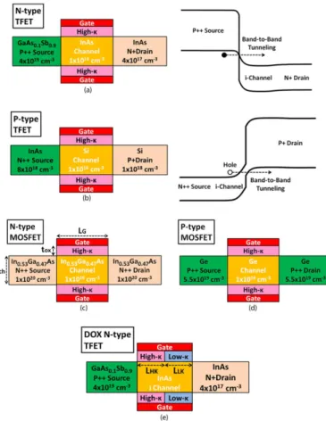
On the other hand, TFET device which utilizes the band-to-band tunneling (BTBT) as the major conduction mechanism is considered to be one of the most promising devices to re-place MOSFET device for ultra-low voltage operation due to its steep ( 60 mV/dec at room temperature) subthreshold slope [4]–[6]. The device structures and band diagrams of N-type TFET and P-type TFET describing the conduction mechanism are shown in Fig. 1(a) and Fig. 1(b), respectively. The superior subthreshold slope and better characteristics of TFET device provides substantial advantages in designing high-speed low-power circuits for operation. However, due to the source-channel barrier in TFET device, the TFET de-vice capacitance is dominated by (Miller capacitance) in the weak and strong inversion region, which is substantially larger than that in the MOSFET device [7]. In MOSFET de-vice, once the inversion channel is formed, the source and drain are “connected” by the conducting inversion channel, and the gate-to-channel capacitance is divided/partitioned into and . For TFET device, due to the source-channel barrier, the gate-to-channel capacitance manifests itself almost entirely as . The large Miller capacitance in TFET device causes significant overshoot and undershoot during circuit switching to degrade the switching delays and dynamic energy consumption, thus undermining the advantage of steep subthreshold slope of TFET devices. From circuit point of view, the Miller capaci-tance of TFET device is of particular imporcapaci-tance and should be reduced. In our previous study [8], the device design tech-niques for improving the device characteristic and reducing of TFET device are investigated. Among the techniques, the Dual Oxide (DOX) approach, where low- gate dielectric is used near the drain side to reduce the Miller capacitance, pro-vides better improvements in both the delay and dynamic en-ergy. In this work, we use DOX TFET devices for 0.2 V circuit designs.
The rest of the paper is organized as follows. Section II de-scribes the device designs and TCAD simulation methodology of hetero-channel TFET and MOSFET devices. Section III evaluates the feasibility of sub-0.2 V high-speed low-power circuits using hetero-channel MOSFET and TFET devices. Four cases are considered: (1) the nominal hetero-channel MOSFET-based circuits, (2) hetero-channel MOSFET-based circuit with dual supply, dual assisted circuits [3], (3) nom-inal hetero-channel TFET-based circuits and (4) hetero-channel TFET-based circuits using DOX TFET devices. Logic circuits
1549-8328 © 2014 IEEE. Personal use is permitted, but republication/redistribution requires IEEE permission. See http://www.ieee.org/publications_standards/publications/rights/index.html for more information.
Fig. 1. Device structure of tied-gate (double-gate) FinFET: (a) N-type TFET and the corresponding ON-state band structure, (b) P-type TFET and the corre-sponding ON-state band structure, (c) N-type MOSFET, (d) P-type MOSFET, and (e) N-type TFET using Dual Oxide (DOX) technique.
including Inverter, NAND, BUS Driver, and Latch are analyzed and evaluated. Section IV discusses the impacts of temperature and process variations on the hetero-channel TFET-based and MOSFET-based logic circuits. Section V concludes the paper. II. DEVICEDESIGNS ANDTCAD SIMULATIONMETHODOLOGY
Hetero-channel MOSFETs with III-V and Ge semiconductors as channel materials are promising candidates for future CMOS technology to replace conventional Si MOSFETs due to their high mobility, and recent studies have demonstrated the suc-cessful fabrication of InGaAs channel (N-type) and Ge channel (P-type) MOSFET devices on the Si substrate [9], [10]. The ter-minology “hetero-channel MOSFET” refers to MOSFET de-vices with non-Si channel (such as III-V or group IV mate-rials) grown on the Si-platform. In this work, we consider the n-InGaAs MOSFET and p-Ge MOSFET devices. On the other hand, smaller bandgap and direct bandgap materials such as III-V compounds are possible choices for boosting TFET per-formance [11], [12]. In this work, we consider the GaAsSb/InAs NTFET and InAs/Si PTFET devices. The device designs and structures of the N-/P-type MOSFET device, N-/P-type TFET device, and TFET device using Dual Oxide (DOX) technique are shown in Fig. 1. FinFET tied-gate (double-gate) structures are used for all five devices in Fig. 1. The device parameters are listed below: channel length , channel
thick-ness , high- gate oxide with
as the gate dielectric and
as the low- gate dielectric , the length of the high- gate oxide and of the low- gate oxide are 5 nm and 17 nm, respectively for DOX TFET. To
accurately assess the device characteristics and circuit behav-iors of high mobility channel n-InGaAs and p-Ge MOSFET de-vices, the mobility model and Schenk band-to-band tunneling (BTBT) model capturing the leakage current are calibrated with the experimental data in [13]–[15] for mixed-mode TCAD sim-ulations [17]. For heterojunction TFET devices, the nonlocal BTBT model which is applicable for arbitrary tunneling barrier with non-uniform electric field is used. The tunneling paths are dynamically determined according to the gradient of the band energy. The band-gap widening due to quantum confinement is considered in this work and the BTBT model parameters, and , which are important material-related factors deter-mining the band-to-band generation rates are referenced from [16] in which these parameters are calibrated with the NEGF (Non-Equilibrium Green’s Functions)-based approach for het-erojunction Tunneling FET devices. The detailed material pa-rameters used in this work are listed in Table I.
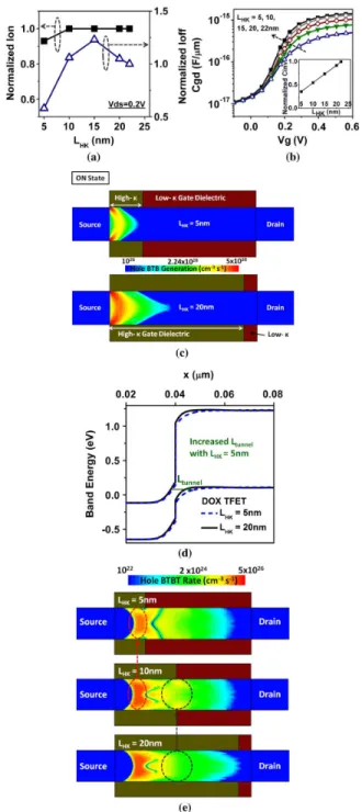
For TFET device, the DOX technique (Fig. 1(e)) uses dif-ferent gate dielectric material at the drain and source side. By placing the high- gate oxide at the source side and low- gate oxide at the drain side, the and can be reduced while retaining the ON-OFF characteristics of the TFET device as shown in Fig. 2(a) and Fig. 2(b). Simulated and with different lengths of high- gate oxide ( ) are shown in Fig. 2(a). The degrades about 7% when shrinks to 5 nm, while shows an inflection point at about half of the channel length. This is because in the ON state, the BTBT oc-curs near the source-channel junction, the shrinkage of in which the energy band of the channel region controlled by the high- gate oxide does not significantly affect the band-to-band tunneling junction. However, as the becomes smaller to 5 nm, the energy band near the source-channel tunnel junction becomes retarded (Fig. 2(d)), resulting in larger tunneling length and thus degrading . The detailed band diagrams showing the increased tunneling length as the decreases and the corresponding Hole-Band-to-Band Tunneling Rate are shown in Fig. 2(c) and Fig. 2(d), respectively. For , as reduces to about half of the channel length, the channel region controlled by the high- gate oxide near the drain side becomes smaller, thus the energy band at the drain side gets retarded, leading to increase as indicated by the gray dashed circle shown in Fig. 2(e). As continues to shrink, the influence of the high- gate oxide on the energy band of the source-channel junction becomes smaller, and starts to decrease due to less BTBT leakage as indicated by
Fig. 2. (a) Normalized Ion-Ioff characteristic with different lengths of high-gate dielectric and (b) Cgd-Vg characteristic of TFET device using dual high-gate oxide (DOX) technique. The inset of (b) shows the improvement with when using the DOX technique. (c) Hole-Band-to-Band Tunneling (BTBT) Rate in the ON state for DOX TFET devices with and 20 nm, respectively. (d) Band diagrams of DOX TFET devices in the ON state with and 20 nm, respectively. (e) Hole-Band-to-Band Tunneling Rate in the OFF state for DOX TFET devices with , 10 nm and 20 nm. The gray dashed circles indicate the increased with
decrease to 10 nm, while the red dashed circles indicate the decreased with decrease to 5 nm.
the red dashed circle shown in Fig. 2(e), thus resulting in the inflection in Fig. 2(a). In Fig. 2(b), we can clearly see that the use of low- gate oxide at the drain side can effectively reduce and , and the reduction of capacitances becomes more pronounced as becomes smaller. As shown in the inset of Fig. 2(b), for , can be reduced to 30% of the nominal of TFET without the DOX technique. From CV/I point of view, the DOX TFET provides substantial
Fig. 3. Id-Vg characteristics of hetero-channel MOSFET and TFET devices.
advantages for improving the circuit performance and energy, in additional to the significant benefit of reducing the over-shoot/undershoot during switching. In this work, we choose for of the DOX TFET. Simulated Id-Vg char-acteristics of the hetero-channel MOSFET and TFET device are shown in Fig. 3. The hetero-channel MOSFET with lower threshold voltage is designed to have the same threshold voltage as that of the N-type TFET device . The higher threshold voltage of the hetero-channel MOSFET
is designed for a target leakage current near . The Id-Vg of the DOX TFET is quite close to the nominal TFET with slight degradation in . Note that here we use constant-current defined threshold voltage, and we adjust the work functions for TFET and MOSFET devices to attain similar threshold voltages.
III. SUB-0.2 V HIGH-SPEEDLOW-POWERCIRCUITS
In this section, high-speed low-power circuits consisting of nominal hetero-channel MOSFET device, hetero-channel MOSFET device with dual supply, dual assisted circuits, nominal hetero-channel TFET device and hetero-channel DOX TFET device are comprehensively analyzed and compared using mixed-mode TCAD simulations for sub-0.2 V operation. In the following sections, the word “hetero-channel” will be omitted for simplicity of description, while it is to be under-stood that “hetero-channel” devices as shown in Fig. 1 are used. A. NAND
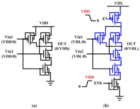
Fig. 4(a) shows the schematics of the conventional two-way NAND structure for the nominal MOSFET, nominal TFET, and DOX TFET, while Fig. 4(b) is the schematics of two-way NAND structure using assist-circuits with dual supply, dual MOSFET devices. In Fig. 4(b), MOSFET devices (indicated by blue colors) are used in the core circuit with lower supply voltage, whereas MOSFET devices are used for the power-gating devices in the assist-circuits with larger input swing to reduce Standby leakage and power. It should be noted that the use of P-type MOSFET power-gating devices [1] is to provide higher driving current. With its large input swing , the Standby leakage current of the internal logic core can be reduced. Without a negative bias VNN, the N-type MOSFET power-gating device should be used to reduce the Standby leakage and power. Fig. 5 shows the transient waveforms of the two-way NAND during switching. The worst-case, bottom-switching pattern is considered. For the NAND structure with power-gating assist-circuit, a core supply
Fig. 4. Schematics of two-way NAND structures of (a) nominal MOSFET de-vice, nominal TFET dede-vice, DOX TFET dede-vice, and (b) MOSFET device with assist circuits using powering-gating devices (indicated by black color).
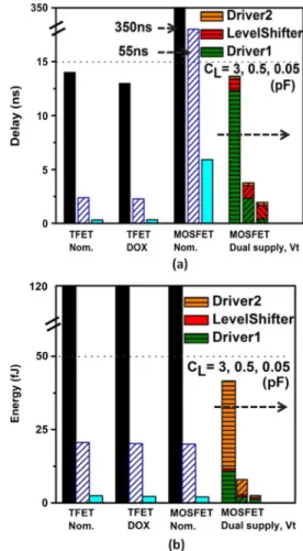
are both considered. Fig. 6(a) and 6(b) show the dynamic energy versus delay and energy-delay product (EDP) versus Standby leakage power of TFET-based and MOSFET-based NAND circuits with two, three and four inputs, respectively. As shown,
the utilization of dual supply , dual
technique improves both the delay and dynamic energy compared with the case using nominal MOSFET devices.
While provides the best delay, it
consumes larger dynamic energy. The nominal TFET devices outperform the nominal MOSFET devices in operational speed due to steeper subthreshold swing and higher drive current at low supply voltage, but suffer from larger dynamic energy due to deteriorated overshoot/undershoot characteristic from Miller capacitance. With the reduced Miller capacitance of DOX TFET, the overshoot is significantly reduced (Fig. 5), resulting in further improvement in delay and dynamic energy compared with the nominal TFET devices. The energy-delay product and Standby leakage power are important metrics for high-speed low-power operation. As shown in Fig. 6(b), the DOX TFET device provides substantial advantages in both the energy-delay product and Standby leakage power. Although MOSFET device with assist-circuit using dual supply
( and ),
dual technique improves the energy-delay product, the cor-responding Standby leakage is one to two orders of magnitude larger compared with the DOX TFET device. Furthermore, the power-gating devices increase the device count and area, and on-chip supply generation circuit (Level Shifter) is needed. For NAND circuits with more number of inputs, the results indi-cate that the degradation of delay becomes more pronounced for both MOSFET and TFET-based NAND circuits. For the cases with four inputs, MOSFET device with assist-circuit
using dual supply , dual
technique provides best delay performance, and DOX TFET shows better delay performance among the others. Regarding the EDP versus leakage power, MOSFET with dual supply , dual assist-circuit with higher number of inputs exhibits best EDP performance but suffer from about two orders larger leakage power compared with the nominal MOSFET and TFET-based NAND circuits. Both the nominal MOSFET-based and DOX TFET-based NAND demonstrates sufficient EDP performance and lower leakage power when considering increased complexity in number of inputs.
Fig. 5. Waveforms of TFET-based and MOSFET-based two-way NAND cir-cuit.
Fig. 6. (a) Dynamic energy versus delay, and (b) Energy-delay product versus Standby leakage power of MOSFET and TFET based NAND circuits with two, three and four inputs.
B. Inverter Chain
Fig. 7(a) shows the schematics of the conventional unloaded three stages inverter chain for nominal MOSFET device,
Fig. 7. Schematics of unloaded three stages inverter chain of (a) nominal MOSFET device, nominal TFET device, DOX TFET device, and (b) MOSFET device with assist circuits using power-gating devices.
Fig. 8. (a) Dynamic energy versus delay, and (b) energy-delay product versus Standby leakage power of MOSFET and TFET based unloaded three stages inverter chain.
nominal TFET device and DOX TFET device. Fig. 7(b) shows the corresponding schematics for MOSFET devices with dual supply, dual assist-circuit.
Fig. 8(a) and 8(b) show the dynamic energy versus delay and the energy-delay product versus Standby leakage power of TFET-based and MOSFET-based unloaded three stages in-verter chain, respectively. Similar to the case for the NAND structure, compared with the nominal MOSFET case, the re-sults indicate that the use of dual supply, dual technique effectively reduces the dynamic energy by approximately 6x, and improves the delay by 36%. The DOX TFET offers the best delay (58% improvement compared with MOSFET with dual supply, dual technique), but suffers from larger dynamic energy due to larger overshoot. MOSFET devices with dual supply, dual assist-circuit exhibit substantial energy-delay product improvement, yet suffer significantly larger Standby leakage power (more than one order of magnitude compared with the nominal MOSFET case).
On the other hand, DOX TFET provides comparable (only slightly larger) energy-delay product and Standby leakage
Fig. 9. Schematics of Bus Driver structures of (a) nominal MOSFET device, nominal TFET device, DOX TFET device, and (b) MOSFET device with assist-circuit using dual supply dual technique.
Fig. 10. (a) Delay and (b) dynamic energy of the TFET-based and MOSFET-based bus driver with different bus line loading.
power compared with the nominal MOSFET, while achieving significant ( 2x) delay improvement.
C. Bus Driver
Fig. 9(a) show the schematics of the conventional bus driver for nominal MOSFET device, nominal TFET device, and DOX TFET device, while Fig. 9(b) is the schematics of bus driver using assist-circuit with dual supply, dual MOSFET devices. For MOSFET-based bus driver, in order to drive the heavy load (bus line with capacitance ) quickly, the level shifter to generate large swing from to is needed. The relative strength of pass transistors, pull-up transistors, and
driver and the DOX TFET-based bus driver provide significant delay improvement without the overhead of assist-circuit. For the dynamic energy, the MOSFET-based bus driver with dual supply, dual assist-circuit is superior than the other three cases. As discussed earlier in this section, the MOSFET-based bus driver with dual supply, dual assist-circuit should be carefully designed to ensure that the energy consumption of the high- circuit is negligibly small compared with the driver and the load. Also, the sized-up Driver1 may contribute a sig-nificant portion of the total dynamic energy and the dynamic en-ergy becomes comparable with the other three cases when becomes lighter.
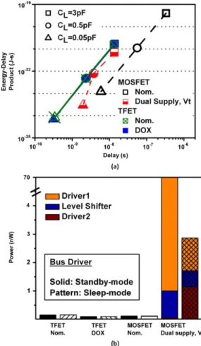
Fig. 11 shows the energy-delay product versus delay of the TFET-based and MOSFET-based bus driver with different bus line loading , respectively. As shown, when the bus line loading is heavy , the MOSFET-based bus driver with dual supply, dual assist-circuit can improve the delay by one order of magnitude and improve the energy-delay product by two orders of magnitude compared with the nom-inal MOSFET bus driver. As the bus line loading becomes lighter , the improvement provided by the dual supply, dual technique decreases, and the delay becomes comparable to the nominal MOSFET bus driver. This is be-cause with light load, the delay is mostly from the level shifter which constrains the improvement of overall bus driver delay as indicated in Fig. 10(a).
On the other hand, as shown in Fig. 11(a), both the nom-inal TFET-based bus driver and DOX TFET-based bus driver can provide comparable delay and energy-delay product to the MOSFET-based bus driver with dual supply, dual assist-cir-cuit, and even outperform under light bus line loading con-dition. Fig. 11(b) shows the Standby power and Sleep-mode power of the TFET-based and MOSFET-based bus driver. Here, the Standby power is defined as the power that the bus driver consumes when the dynamic operation is OFF and the power-gating devices are ON. The Sleep-mode power is defined as the power that the bus driver consumes when the dynamic oper-ation and the power-gating devices are both OFF. As shown, the nominal MOSFET-based, nominal TFET-based, and DOX TFET-based bus driver have comparable Standby power and Sleep-mode power, while the MOSFET-based bus driver with dual supply, dual assist-circuit exhibits Standby power three orders of magnitude larger and Sleep-mode power near two or-ders of magnitude larger. The large Standby power consumption comes mainly from the assist-circuit, namely the level shifter and Driver1. For the Sleep-mode, although the power-gating de-vices in the OFF-state can reduce the power by 23x compared with the Standby-mode, Driver1 and Driver2 still have larger leakage compared with the other three cases.
Fig. 11. (a) Energy-delay product versus delay with square symbol indicates , circle symbol indicates , and triangle indicates . (b) Standby power (indicated by solid bars) and Sleep-mode power (indicated by pattern bars) of the TFET-based and MOSFET-based bus driver with different bus line loading.
D. Latch
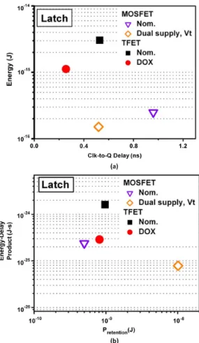
Here we consider the Clocked-CMOS Latch instead of the Transmission Gate Latch due to its better stability in low voltage operation [18]. Fig. 12(a) shows the schematics of the Clocked-CMOS Latch circuit for nominal MOSFET, nominal TFET, and DOX TFET, while Fig. 12(b) is the schematics of Latch for MOSFET with dual supply, dual assist-circuit technique. The dynamic energy versus clock-to-Q delay for each case are shown in Fig. 13(a). The energy-delay product versus the power in retention mode are shown in Fig. 13(b). As shown, the DOX TFET-based latch has energy-delay pro-dutct and retention-mode power comparable to the nominal MOSFET-based latch. The MOSFET-based latch with dual supply, dual technique shows better energy-delay product, but suffers from one order of magnitude larger retention-mode power compared with the nominal MOSFET-based latch. Also, the power-gating devices in MOSFET-based latch with dual supply, dual technique should be carefully designed to ensure the data integrity in the retention mode. Table II shows the total fin number used in MOSFET-based and TFET-based Bus Driver and CMOS-Clocked Latch. The large fin number required for the MOSFET-based design with dual-supply dual- assist-circuit can be clearly seen.
IV. IMPACTS OFTEMPERATURE ANDPROCESSVARIATIONS
In this section, the impacts of temperature and process vari-ations on TFET-based and MOSFET-based NAND circuits are discussed.
Fig. 12. Schematics of Clocked CMOS Latch of (a) nominal MOSFET device, nominal TFET device, DOX TFET device, and (b) MOSFET device with assist-circuit using dual supply dual technique.
Several simulation-based and experimental studies have investigated the impact of temperature variations on the Tun-neling FET devices and MOSFET devices [19], [20]. These studies indicate that TFET device shows distinct behavior and weak temperature variability compared with MOSFET devices. It is believed that the current of TFET would increase slightly due to the weak temperature dependence of band-gap narrowing as temperature increases. For MOSFET devices, on the other hand, the temperature dependence of the current results from two sources: mobility, and threshold voltage. The ON state current would decrease and shows larger variability with increasing temperature owing to the phonon scattering in the channel. While the threshold voltage would decrease hence the current would increase with increasing temperature. Hence, the TFET-based logic circuits are expected to exhibit less temperature variability compared with the MOSFET-based logic circuits.
For process variations, deviations in device parameters such as , and are considered to assess process-induced variability in TFET-based and MOSFET-based circuits. For each process parameters, devices with 10% variations from its nominal value are considered at high drain bias condition ( ; while for dual supply dual MOSFET,
Fig. 13. (a) Dynamic energy versus clock-to-Q delay, and (b) energy-delay product versus the power in retention mode for TFET-based and MOSFET-based Clocked CMOS Latch.
TABLE II
TOTALFINNUMBER OF THETFET-BASED ANDMOSFET-BASEDBUSDRIVER ANDCLOCKED-CMOS LATCH
), and the parameters whose variation cause the largest deviation of the drain current at device level are chosen and used for the circuit simulations. In our analysis, varia-tion causes the most pronounced variability in drive current for TFET devices while for MOSFET devices, results in the largest current variability.
The simulated energy versus delay of TFET-based and MOSFET-based two-way NAND and three-way NAND cir-cuits considering the process variations are shown in Fig. 14(a) and Fig. 15(a) where the error bar indicates circuit variability caused by the dominant process variation source. The simulated energy-delay product (EDP) versus power of TFET-based and MOSFET-based two-way NAND and three-way NAND cir-cuits considering the process variations are shown in Fig. 14(b) and Fig. 15(b) where the nominal case is indicated by solid
Fig. 14. (a) Dynamic energy versus delay and (b) energy-delay product versus the power of MOSFET and TFET based two-way NAND circuits considering the process variations. The variability caused by the process variations are in-dicated with error bar in (a) and by hollow symbols in (b).
symbols and the process variation caused variability is indi-cated by hollow symbols.
In Fig. 14(a), TFET-based two-way NAND circuits show smaller variation in delay compared with the MOSFET-based two-way NAND circuits. Also, the MOSFET circuit with dual supply dual assist-circuit shows the largest variation in dynamic energy. TFET-based two-way NAND circuits show smaller variation in EDP but slightly larger variation in leakage power consumption. For three-way NAND circuits, the four topologies all exhibit larger variability due to larger device counts compared with the two-way NAND circuits. The result shows similar trends as the two-way NAND circuits but with larger variability.
V. CONCLUSION
We present a comprehensive evaluation of the feasibility of sub-0.2 V high-speed low-power circuits with hetero-channel MOSFET and TFET devices using TCAD mixed-mode sim-ulations. The delay, dynamic energy, and Standby power of the TFET-based and MOSFET-based logic circuits including NAND, Inverter, BUS Driver, and Latch are analyzed and compared. The results indicate that for the logic circuits in-cluding the NAND, Inverter chain, and Latch circuits, nominal TFET-based circuits provide significant improvement in delay compared with the nominal MOSFET-based circuits. However,
Fig. 15. (a) Dynamic energy versus delay and (b) energy-delay product versus the power of MOSFET and TFET based three-way NAND circuits considering the process variations. The variability caused by the process variations are in-dicated with error bar in (a) and by hollow symbols in (b).
due to the large Miller capacitance in Tunnel FET devices, the dynamic power is larger than the nominal MOSFET-based circuits, hence would have larger EDP (energy-delay product). With the DOX device design, the dynamic energy is greatly improved with the nominal TFET-based circuits. The DOX TFET-based circuits have comparable EDP and Standby power in NAND, inverter chains and Clocked-CMOS Latch com-pared with the nominal MOSFET-based circuits. While the MOSFET-based circuits using assist-circuits with dual supply, dual technique improve the delay and dynamic energy at the expense of the device count, circuit area, and large leakage power in Standby and Sleep-mode. For the Bus Driver circuits, both the nominal and DOX TFET-based circuits outperform the nominal MOSFET-based circuits in EDP by about two orders of magnitude and consume comparable Standby power. On the other hand, the MOSFET-based circuits using assist-circuits with dual supply, dual technique have comparable EDP at the expense of the complicated sizing in contention devices, device count, circuit area, and large leakage power in Standby mode. The TFET-based circuits with DOX device design provides the potential to achieve high-speed low-power circuit
operation at .
ACKNOWLEDGMENT
The authors thank the National Center for High-Performance Computing in Taiwan for the software and facilities.
REFERENCES
[1] A. Tajalli and Y. Leblebici, “Design trade-offs in ultra-low-power dig-ital nanoscale CMOS,” IEEE Tran. Circuits Syst.–I: Reg. Papers, vol. 59, no. 4, pp. 749–762, Apr. 2012.
[2] K. Itoh, “Adaptive circuits for the 0.5-V nanoscale CMOS era,” ISSCC
Dig. Tech, pp. 14–20, Feb 2009.
[3] A. Kotabe, K. Itoh, R. Takemura, R. Tsuchiya, and M. Horiguchi, “Device-conscious circuits design for 0.5-V high-speed memory-rich nanoscale CMOS LSIs,” CICC Dig., vol. 16, no. 1, Sep. 2011. [4] K. Boucart and A. M. Ionescu, “Double-gate tunnel FET with high-k
gate dielectric,” IEEE Trans. Electron Devices, vol. 54, no. 7, pp. 1725–1733, Jul. 2007.
[5] Q. Zhang, W. Zhao, and A. Seabaugh, “Low-subthreshold-swing tunnel transistors,” IEEE Electron Devices Lett. , vol. 27, no. 4, pp. 297–300, 2006.
[6] W. Y. Choi, B.-G. Park, J. D. Lee, and T.-J. K. Liu, “Tunneling field-effect transistors (TFETs) with subthreshold swing (SS) less than 60 mV/dec,” IEEE Trans. Electron Devices, vol. 28, no. 8, pp. 743–745, 2007.
[7] S. Mookerjea, R. Krishnan, S. Datta, and V. Narayanan, “Effective ca-pacitance and drive current for tunnel FET (TFET) CV/I estimation,”
IEEE Trans. Electron Devices, vol. 56, no. 9, pp. 2092–2098, Sep.
2009.
[8] Y.-N. Chen, M.-L. Fan, Vita, P.-H. Hu, P. Su, and C.-T. Chuang, “Investigate of tunneling FET device designs for improving circuit switching performance and energy,” Solid State Devices Mater., Sep. 2013.
[9] S. Takagi and M. Takenaka, “High mobility CMOS technologies using III-V/Ge channels on Si platform,” in Proc. Int. Ultimate Integr. Silicon
Conf., 2012, pp. 1–4.
[10] L. Hutin, C. Royer, J. Damlencourt, J. Hartmann, H. Grampeix, V. Mazzocchi, C. Tabone, B. Previtali, A. Pouydebasque, M. Vinet, and O. Faynot, “GeOI pMOSFETs scaled down to 30-nm gate length with record off-state current,” IEEE Electron Device Lett., vol. 31, no. 3, pp. 234–236, 2010.
[11] D. K. Mohata, R. Bijesh, Y. Zhu, M. K. Hudait, R. Southwick, Z. Chbili, D. Gundlach, J. Suehle, J. M. Fastenau, D. Loubychev, A. K. Liu, T. S. Mayer, V. Narayanan, and S. Datta, “Demonstration of im-proved heteroepitaxy scaled gate stack and reduced interface states en-abling heterojunction tunnel FETs with high drive current and high on-off ratio,” in Proc. Symp. VLSI Tech., 2012, pp. 53–54.
[12] K. E. Moselund, H. Schmid, C. Bessire, M. T. Bjork, H. Ghoneim, and H. Riel, “InAs-Si nanowire heterojunction tunnel FETs,” IEEE
Elec-tron Device Lett., vol. 33, no. 10, pp. 1453–1455, 2012.
[13] L. Hutin et al., “GeOI pMOSFETs scaled down to 30-nm gate length with record off-state current,” IEEE Electron Device Lett., vol. 31, no. 3, pp. 234–236, 2010.
[14] E. Batail et al., “Localized ultra-thin GeOI: An innovative approach to germanium channel MOSFETs on bulk Si substrates,” IEDM Tech.
Dig., pp. 397–400, 2008.
[15] M. Poljak et al., “Features of electron mobility in ultrathin-body In-GaAs-On-Insulator MOSFETs down to body thickness of 2 nm,” in
Proc. IEEE SOI Conf., 2011.
[16] V. Saripalli, A. Mishra, S. Datta, and V. Narayanan, “An energy-ef-ficient heterogeneous CMP based on hybrid TFET-CMOS cores,” in
Proc. Design Automat. Conf., 2011, pp. 729–734.
[17] “Sentaurus TCAD Manual,” .
[18] S. Jain, S. Khare, S. Yada, V. Ambili, P. Salihundam, S. Ramani, S. Muthukumar, M. Srinivasan, A. Kumar, S. K. Gb, R. Ramanarayanan, V. Erraguntla, J. Howard, S. Vangal, S. Dighe, G. Ruhl, P. Aseron, H. Wilson, N. Borkar, V. De, and S. Borkar, “A 280 mV-t0–1.2 V wide-operating-range IA-32 processor in 32 nm CMOS,” ISSCC Dig.
Tech, pp. 66–67, 2012.
[19] R. Narang, M. Saxena, R. S. Gupta, and M. Gupta, “Impact of tem-perature variations on the device and circuit performance of tunnel FET: A simulation study,” IEEE Trans. Nanotechnol., vol. 12, no. 6, pp. 951–957, Nov. 2013.
[20] S. Migita, K. Fukuda, Y. Morita, and H. Ota, “Experimental demon-stration of temperature stability of Si-tunnel FET over Si-MOSFET,” in Proc. Silicon Nanoelectron. Workshop, 2012, pp. 1–2.
Yin-Nien Chen received the B.S. degree from
National Tsing Hua University, Hsinchu, Taiwan, in 2009. She is currently working toward the Ph.D. degree in the Institute of Electronics and Department of Electronics Engineering, National Chiao Tung University, Hsinchu, Taiwan.
Her current research interests include the design and analysis of ultralow power logic circuits and SRAMs in nanoscaled technologies.
Ming-Long Fan (S’09) received the B.S. and M.S.
degrees from National Chiao Tung University, Hsinchu, Taiwan, respectively, where he is currently working toward the Ph.D. degree in the Institute of Electronics and Department of Electronics Engi-neering.
His current research interests include the design and optimization of low-power logic and static random access memory in scaled/exploratory tech-nologies.
Vita Pi-Ho Hu (S’09–M’13) received the Ph.D.
degree from the Institute of Electronics and Depart-ment of Electronics Engineering, National Chiao Tung University (NCTU), Hsinchu, Taiwan, in 2011. She is currently an Assistant Researcher with NCTU.
Pin Su (S’98–M’02) received the B.S. and M.S.
de-grees in electronics engineering from National Chiao Tung University (NCTU), Hsinchu, Taiwan, and the Ph.D. degree from the Department of Electrical En-gineering and Computer Sciences, University of Cal-ifornia at Berkeley, Berkeley, CA, USA.
From 1997 to 2003, he conducted his doctoral and postdoctoral research in Silicon-On-Insulator (SOI) devices at Berkeley. He was also one of the major contributors to the unified BSIMSOI model, the first industrial standard SOI MOSFET model for circuit design. Since August 2003, he has been with the Department of Electronics Engineering, NCTU, where he is currently a Professor. His research interests include silicon-based nanoelectronics, modeling and design for exploratory CMOS devices for ultra-low-power applications, and circuit-device interaction and co-optimization in nanoscale CMOS. He has authored or coauthored over 70 refereed journal papers and 100 conference papers regarding his research interests.
Ching-Te Chuang (S’78–M’82–SM’91–F’94) received the B.S.E.E.degree from National Taiwan University, Taipei, Taiwan, in 1975, and the Ph.D. degree in electrical engineering from the University of California at Berkeley, Berkeley, CA, USA, in 1982.
From 1982 to 2008, he was with the IBM T. J. Watson Research Center, Yorktown Heights, NY, USA, holding various technical and management positions. He joined the Department of Electronics Engineering, National Chiao Tung University, Hsinchu, Taiwan, in 2008, where he is currently a Life Chair Professor. He has authored or coauthored over 370 papers. He holds 54 U.S. patents with another 20 pending.