2
‑Alkyl-5-thienyl-Substituted Benzo[1,2‑b:4,5‑b′]dithiophene-Based
Donor Molecules for Solution-Processed Organic Solar Cells
Dhananjaya Patra,
†Tzu-Yen Huang,
†,‡Chao-Cheng Chiang,
†Ramon Orlando Valencia Maturana,
†Chun-Wei Pao,
†Kuo-Chuan Ho,
‡,§Kung-Hwa Wei,
∥and Chih-Wei Chu*
,†,⊥†Research Center for Applied Sciences, Academia Sinica, Taipei, Taiwan (ROC)
‡Department of Chemical Engineering, National Taiwan University, Taipei, Taiwan (ROC) §Institute of Polymer Science and Engineering, National Taiwan University, Taipei, Taiwan (ROC)
∥Department of Materials Science and Engineering, National Chiao-Tung University, Hsinchu, Taiwan (ROC) ⊥Department of Photonics, National Chiao-Tung University, Hsinchu, Taiwan (ROC)
*
S Supporting InformationABSTRACT: In this study, we have strategically designed and convergently synthesized two novel, symmetrical, and linear A− D−A-type π-conjugated donor molecules (TBDTCNR, TBDTCN), each containing a planar electron-rich 2-octylthiene-5-yl-substituted benzodithiophene (TBDT) unit as the core,flanked by octylthiophene units and end-capped with electron-deficient cyanoacetate (CNR) or dicyanovinyl (CN) units. We thoroughly characterized both of these materials and investigated the effects of the end groups (CNR, CN) on their optical, electrochemical, morphological, and photovoltaic properties. We then fabricated solution-processed bulk heterojunction organic solar cells incorporating TBDTCNR and TBDTCN. Among our tested devices, the one containing TBDTCNR and [6,6]-phenyl-C61-butyric acid methyl ester in a 1:0.40 ratio (w/w) exhibited the highest power conversion efficiency (5.42%) with a short-circuit current density (Jsc) of 9.08 mA cm−2, an open circuit voltage (Voc) of 0.90 V, and an impressivefill factor (FF) of 0.66 under AM 1.5G irradiation (100 mW cm−2). The FFs of these solution-processed small-molecule organic solar cells (SMOSCs) are outstanding when compared with those recently reported for benzodithiophene (BDT)-based SMOSCs, because of the high crystallinity and excellent stacking properties of the TBDT-based compounds.
KEYWORDS: solution-processed small-molecule, donor−acceptor, organic solar cells, power conversion efficiency, benzo[1,2-b:4,5-b′]dithiophenes, external quantum efficiency
1. INTRODUCTION
Solution-processed polymer solar cells (PSCs) are emerging as promising alternatives to silicon-based solar cells; they provide enormous benefits as a result of their low cost, amenability, high-throughput roll-to-roll processing, and ready structural modifications.1−5 Recently, tremendous research efforts have been devoted to the development of π-conjugated small molecules for use in bulk heterojunction (BHJ) solar cells, the power conversion efficiencies (PCEs) of which have dramatically increased to over 8%.6,7 Although the PCEs of solution-processed small molecule organic solar cells (SMOSCs) have not matched those achieved by PSCs, their
many advantages ready synthesis, high purity and crystallinity, well-defined molecular structures, lack of end group contam-inants, high mobility, and batch-to-batch consistency cannot be ignored.8−10Some spectacular results have been demonstrated recently for SMOSCs, suggesting that they might soon become better alternatives to PSCs in the quest to meet global energy challenges.6,8,9 Nevertheless, research into SMOSCs requires much further attention if we are to solve their shortcomings
Received: June 10, 2013
Accepted: September 3, 2013
Published: September 3, 2013
namely, low fill factors (FFs), poor film quality and morphology, and unbalanced charge transport relative to that of PSCs.11,12To overcome these challenges, it will be necessary to develop novel alternating donor−acceptor (D−A) building blocks using a design strategy similar to that for PSCs.
Substantial progress has been made in the fabrication of SMOSCs incorporating small molecules featuring different D and A units, including oligothiophene,13 triphenylamine,14 dithienosilole,6 benzodithiophene,7 benzotrithiophene,15 ben-zothiadiazole,16 diketopyrrolopyrole,17 cyanoacetates,18 dicya-novinyl,19 and rhodanine7 moieties, in novel molecular frameworks (e.g., D−A−D, A−D−A, D−A−A, D−A−D−A− D). Because of their efficient light harvesting, face-to-face π−π stacking, structural versatility, and superior charge transport behavior and solar cell performance, fused thiophene-based A− D−A architectures containing cyanoacetate (CNR) and dicyanovinyl (CN) units have recently gained considerable attention.18−21 Indeed, when Chen and coworkers prepared SMOSCs incorporating small molecules featuring benzodithio-phene (BDT)-based moieties as the central-donating core and end-capped with CNR groups, they achieved PCEs of up to 5.54%.18 Bäuerle and coworkers recently reported several oligothiophenes and alkylthiophenes end-capped with CN units that they use to prepare vacuum- and solution-processed solar cells displaying impressive performance.19,21 Chen and cow-orkers also reported another successful SMOS incorporating a planar molecule featuring a BDT unit as the electron-donating core surrounded by alkylthiophene units and terminated with rhodanine as the electron acceptor that displayed a PCE of 8.12%;7 here, the lateral modification of the BDT core with alkylthiophene units extended the electron donating capability and solubility of theπ-conjugated moiety. Hou and Yang et al. prepared 2-alkyl-5-thienyl-substituted benzo[1,2-b:4,5-b ′]-dithiophenes (TBDTs) coplanar,π−π stacking, high-mobility, sulfur-rich, electron-donating alternatives to BDT that provided SMOSCs displaying excellent performance relative to PSCs.22 Moreover, TBDT-type compounds exhibit low-energy highest occupied molecular orbitals (HOMOs) potentially providing high open circuit voltages and energy levels of lowest unoccupied molecular orbitals (LUMOs) that can be manipulated effectively through the use of various accept-ors.7,22,23
Herein, we report the design and synthesis of two small molecules (TBDTCNR, TBDTCN), each containing TBDT as the central electron donor unitflanked by octylthiophene units and end-capped with CNR or CN acceptors. The nature of the acceptor end group affects the intermolecular interactions of TBDTCNR and TBDTCN and, thereby, their bulk properties, including their optical, electrochemical, X-ray diffraction (XRD), and photovoltaic properties. Among our tested systems, the best BHJ solar cell device incorporating a blend of TBDTCNR and [6,6]phenyl-C61-butyric acid methyl ester (PC61BM) at a ratio of 1:0.4 delivered the highest PCE (5.42%).
2. EXPERIMENTAL SECTION
2.1. Fabrication and Characterization of Organic Solar Cells (OSCs). The solution-processed small-molecule BHJ solar cells featured a thin film of the active layer, a blend of the donor (TBDTCNR or TBDTCN) and acceptor (PC61BM) materials, sandwiched between a transparent anode (ITO) and a metal cathode. Prior to device fabrication, the ITO glasses (1.5 × 1.5 cm2) were cleaned ultrasonically with detergent, deionized water, acetone, and isopropyl alcohol. After routine solvent cleaning, the ITO substrates
were treated with UV ozone for 15 min and then spin-coated with the PEDOT:PSS layer (∼30 nm) at 4000 rpm. The active layer solution, TBDTCNR/PC61BM or TBDTCN/PC61BM (8 mg mL−1for donor materials in CHCl3), was then cast upon the modified ITO substrate. Thermal annealing treatment was performed at various temperatures from 75 to 125°C for 30 min to pre-anneal the active layer. After preparing the active layer, Ca (30 nm) and Al (100 nm) were evaporated onto the active layer under vacuum (pressure = <6× 10⁻⁶ Torr) through a shadow mask to form the cathodes. The active area of the devices was 0.1 cm2. The active layer thickness was measured using an AlphaStep profilometer (Veeo, Dektak 150). The photovoltaic performance was characterized within a N2-filled glove box under an AM 1.5Gfilter (100 mW cm−2) using a Newport Oriel Solar Simulator (Thermal Oriel 1000W), as calibrated using a Si photodiode. All electric testing was performed within N2-filled glove boxes using an HP 4145C semiconductor parameter analyzer. EQEs were measured by comparing the photocurrent of a sample device and that of a standard Si device at various wavelengths of incident light. The light source was a 450 W Xe lamp (Oriel Instrument, model 6266) equipped with a water-based IR filter (Oriel Instrument, model 6123NS). The light output from the monochromator (Oriel Instrument, model 74100) was focused onto the PV devices.
2.2. Fabrication of Hole- and Electron-Only Devices. The configurations of the hole- and electron-only devices were ITO/ PEDOT:PSS/small molecule:PC61BM/V2O5/Al and ITO/Cs2CO3/ small molecule:PC61BM/Ca/Al, respectively. The electron and hole motilities were determined byfitting the plots of the dark J−V curves for single-carrier devices to the SCLC model.24The dark current was given by
ε ε μ
=
J 9 0 r V2/8L3
whereεris the relative dielectric constant of the transport medium,ε0 is the permittivity of free space,μ is the carrier mobility, and L is the device thickness.
3. RESULTS AND DISCUSSION
3.1. Synthesis and Thermal Properties. Scheme 1 presents the synthetic route we followed to prepare TBDTCNR and TBDTCN. We performed the syntheses of most of the intermediates (compounds 1−7) using slight modifications of procedures reported in the literature.18,21 Symmetrical Stille coupling of 3 and 7 yielded compound 8, which we subjected to Knoevenagel condensation to generate TBDTCNR and TBDTCN. Both TBDTCNR and TBDTCN were highly soluble in common organic solvents (e.g., CH2Cl2, CHCl3, and THF) and exhibited good thermal stability up to 365°C under a N2atmosphere (Supporting Information Figure S3). The melting point of TBDTCNR and TBDTCN found to Figure 1.Chemical structures of TBDTCNR and TBDTCN.
be 177 and 207 °C (Supporting Information Figure S3), respectively.
3.2. Optical Properties. Figure 2 displays normalized UV− vis absorption spectra of dilute solutions of TBDTCNR and
TBDTCN in CHCl3and of their solidfilms spin-coated onto glass substrates; Table 1 lists the normalized absorption maxima for both the solutions and solidfilms and their optical band gaps (Egopt). In solution, both TBDTCNR and TBDTCN exhibited two characteristic bands: a shorter-wavelength absorbance arising from π−π* transitions and a longer-wavelength band that we attribute to intramolecular charge transfer (ICT) between the rich TBDT and electron-deficient (CNR or CN) segments.16 The absorption band of TBDTCNR in solution was located at 488 nm. In contrast, the absorption spectrum of TBDTCNR as a solid film exhibited localization of its transition and ICT bands, which overlapped to form a new broad band at 578 nm and a bathochromic shift of approximately 90 nm relative to that in solution, due to effective π−π interactions.18The absorption band of TBDTCN in solution and in the solidfilm appeared at 494 (shoulder) and 590 nm, respectively; again, the latter exhibited a bathochromic shift of approximately 96 nm relative to the former, as well as broadening of the ICT band as a result of strong π−π interactions.13,25 The presence of highly electron withdrawing CN groups at both ends of the TBDT unit led to bathochromic shifts of 6 and 12 nm relative to the signals of the CNR-presenting TBDT derivative in solution and in the solidfilm, Scheme 1. Synthesis of TBDTCNR and TBDTCNa
aReagents and conditions: (i) 2-octylthiophene, n-BuLi, THF, 1 h; then compound 1, 50°C, 1 h; then SnCl
2/HCl/H2O, 50°C, 2 h; (ii) n-BuLi, THF,−78 °C, 1 h; then SnMe3Cl; (iii) trimethyl(4-octylthien-2-yl)stannane, Pd(PPh3)4, toluene, reflux; (iv) NBS, CHCl3/AcOH (1:1), 0°C then RT overnight; (v) Pd(PPh3)4, toluene, reflux; (vi) CHCl3, piperidine, octyl cyanoacetate, RT, 36 h; or CHCl3, piperidine, malononitrile, RT, 36 h.
Figure 2.Normalized UV−vis absorption spectra of TBDTCNR and TBDTCN as dilute solutions in CHCl3 and as thin films on glass surfaces at room temperature.
Table 1. Optical and Electrochemical Properties of TBDTCNR and TBDTCN
solutiona solidfilmb energy levels band gapsd
SM λmax,abs(nm) λmax,abs(nm) Eonsetox(V)/HOMOc(eV) Eonsetred(V)/LUMOc(eV) Egec(eV) Egopt(eV)
TBDTCNR 488 578 1.05/−5.40 −0.72/−3.63 1.77 1.75
TBDTCN 433, 494 590 1.10/−5.45 −0.74/−3.61 1.84 1.72
aIn THF dilute solution.bSpin-coated from THF solution onto a glass surface.cE
HOMO/ELUMO= [−(Eonset− Eonset (FC/FC+vsAg/Ag+))− 4.8] eV,where 4.8 eV is the energy level of ferrocene below the vacuum level and the formal potential Eonset (FC/FC+vsAg/Ag+)is equal to 0.45 V.dElectrochemical band gap: Egec= Eox/Onset− Ered/Onset; optical band gap: Egopt= 1240/λedge.
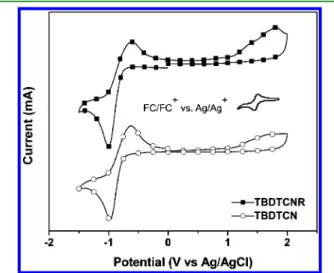
respectively. We calculated the optical band gaps for TBDTCNR and TBDTCN, from the onsets of the signals in the absorption spectra of the thinfilms, to be 1.75 and 1.72 eV, respectively. The broad features in the absorption spectra of TBDTCNR and TBDTCN suggested that both compounds would be effective candidates for application in BHJ solar cells. 3.3. Electrochemical Properties. We used cyclic voltammetry (CV) to investigate the electrochemical properties of TBDTCNR and TBDTCN; Figure 3 presents their
oxidation and reduction cyclic voltammograms and Table 1 summarizes the data. TBDTCNR and TBDTCN both underwent oxidation (p-doping), because of their electron-rich TBDT units, in positive potential ranges and reduction (n-doping), because of their electron-poor CNR and CN units, in negative potential ranges.26 The onset oxidation potentials (Eoxonset) for TBDTCNR and TBDTCN were 1.05 and 1.10 V, respectively, while their onset reduction potentials (Eredonset) were −0.72 and −0.74 V, respectively. We estimated the HOMO and LUMO energy levels from the oxidation and reduction potentials and the reference energy level of ferrocene (4.8 eV below the vacuum level) according to the equations27
= − − + + −
EHOMO/LUMO [ (Eonset Eonset(FC/FC vsAg/Ag )) 4.8] eV and
=E − E
band gap onsetox onsetred
where the formal potential Eonset(FC/FC+
vsAg/Ag+)is equal to 0.45 V. Consequently, the calculated HOMO and LUMO energy levels for TBDTCNR were−5.40 and −3.63 eV, respectively, and those for TBDTCN were −5.45 and −3.61 eV, respectively. The electrochemical band gaps, calculated from the oxidation and reduction potentials, were approximately 1.77 eV for TBDTCNR and 1.84 eV for TBDTCN. TBDTCN possessed a relatively low HOMO energy level relative to that of TBDTCNR, due to its high onset oxidation potential resulting from the presence of its more highly electron deficient CN units.28,29 The LUMO energy levels of TBDTCNR and TBDTCN were dependent upon the strength of their accepting moieties.30 We anticipated that the low-lying HOMO energy levels of these two TBDT-based compounds would provide higher open circuit voltages (Voc) for their BHJ solar cells incorporating PC61BM as an acceptor, because the value of Voc
depends on the difference between the HOMO energy level of the donor and the LUMO energy level of the acceptor.19The LUMO energy levels of TBDTCNR and TBDTCN (−3.63 and −3.61 eV, respectively) are positioned approximately 0.3 eV above the LUMO energy level of PC61BM, thereby suggesting energetically favorable electron transfer from the donor units to the acceptor units.24,30 The electrochemical band gaps, which were in good agreement with the optical band gaps, were in the desirable range for organic photovoltaic applications.
3.4. Theoretical Calculation. We used density functional theory (DFT) to investigate the geometry and energy levels of TBDTCNR. Supporting Information Table S1 lists the HOMO and LUMO energy levels and the theoretical band gap of TBDTCNR that we determined from our DFT calculations of a single molecule in a vacuum. These values are in reasonable agreement with the experimental values determined using CV. We attribute the slight discrepancy in the theoretical and experimental band gaps to the presence of solvent molecules in the CV experiment. Supporting Information Figure S6 displays the relaxed molecular structure (upper panel), the HOMO electron density (middle panel), and the LUMO electron density (lower panel) of TBDTCNR. The HOMO orbital has its greatest contributions from the central TBDT and neighboring thiophene rings, whereas the LUMO orbital has a significant contribution from the side thiophene rings and the capped CNR groups, indicating a typical A−D−A architecture. We suspect that when the system is oxidized, an electron is removed from the central TBDT ring, but when the system is reduced, the electron has a probability of appearing in the side thiophene rings or the CNR groups.
3.5. XRD. To investigate the molecular order and packing in the films of these materials, we recorded XRD patterns of TBDTCNR and TBDTCN after they had been spin-coated from CHCl3. Figure 4 reveals that the solidfilms of TBDTCNR
and TBDTCN were highly ordered because of their crystalline behavior. The XRD patterns for the solidfilms of TBDTCNR and TBDTCN exhibited similar strong first-order (100) diffraction peaks at values of 2θ of 3.6 and 3.9°, respectively, corresponding to d100-spacings of 23.0 and 22.6 Å, respectively. The d100-spacing is the distance between the main conjugated chains of the small molecules, separated by their side chains; Figure 3.Cyclic voltammograms of TBDTCNR and TBDTCN as thin
films (scan rate = 100 mV s−1).
Figure 4. XRD patterns of TBDTCNR and TBDTCN films spin-coated from CHCl3. Inset: Expanded view of the pattern for TBDTCNR and TBDTCN in the range 6−14 Å.
our solution-processed small molecules feature many alkyl side chains around the main chain, leading to the highly intense first-order (100) diffraction peaks, which were similar to those observed for poly(3-octylthiophene) (P3OT, 20.1 Å) and recently reported some BDT based SMOSCs.7,18,31 The second-order (200) and third-order (300) diffraction peaks for the thinfilm of TBDTCNR appeared at values of 2θ of 7.4° and 11.1°, respectively, corresponding to a d200-spacing of 11.0 Å and a d300-spacing of 7.0 Å. Relative to the signals for the solidfilm of TBDTCN, the second-order (200) and third-order (300) diffraction peaks were almost invisible. This result implies that TBDTCNR undergoes strongπ−π stacking of its main chain and provides a well-organized lamellar structure.31 From the XRD data, we conclude that the crystallinity of TBDTCNR is greater than that of TBDTCN, potentially benefiting the transport of carriers and enhancing the short-circuit current after its incorporation into organic solar cell devices. The strongπ−π stacking ability of TBDTCNR would presumably remain after its incorporation into the active layer of a device, potentially providing a high FF.
3.6. Photovoltaic Properties. We fabricated BHJ solar cells after spin-coating blends from CHCl3solutions at various small molecule to PC61BM ratios, with a device structure of indium tin oxide (ITO)/poly(3,4-ethylenedioxythiophene):po-lystyrenesulfonate (PEDOT:PSS)/small molecule:PC61BM/ Ca/Al. We examined the effects of the spin rate (from 1000 to 4000 rpm) and the pre-annealing temperature on the device performance (Supporting Information Figure S7 and Table S2), which we measured under AM 1.5 illumination (100 mW cm−2). Figure 5 presents the detailed current density−voltage (J−V) characteristics of TBDTCNR and TBDTCN; Table 2 summarizes the corresponding device parameters. The devices incorporating TBDTCNR and TBDTCN displayed high values of Voc (∼0.9 V), because of their low-lying HOMO energy levels, but their optimized PCEs were obtained at different small molecule to PC61BM ratios. A photovoltaic device containing TBDTCNR and PC61BM at a blend ratio of 1:0.25 (w/w) exhibited a value of Vocof 0.90 V, a value of Jscof 6.35 mA cm−2, a FF of 65%, and a PCE of 3.69%; at a weight ratio of 1:0.4, these values were improved to 0.90 V, 9.08 mA cm−2, 66%, and 5.42%, respectively. Although the cell efficiency decreased upon further increasing the amount of PC61BM, the FFs of cells remain above 55%. This high performance suggests that TBDTCNR not only was highly miscible with PC61BM to form nanoscale phase separations at the D−A interfaces for dissociation of the generated excitons by minimized recombi-nation but also displayed good π−π stacking ability and enhance the charge transport and the carrier collection efficiency, resulting in reasonable photogenerated currents and FFs. These devices incorporating TBDTCNR provide the one of the best FFs (66%) among all recently reported BDT-based solution-processable small-molecule solar cells prepared without additives or thermal treatment.7,10−12,18,32,33Moreover, various recent works reported by Chen et al. obtained the highest FF 72% in SMOSCs after addition of additives or without additives or thermal treatment or modified device architecture.7,34 On the other hand, the PCE of the photovoltaic device incorporating TBDTCN and PC61BM at a weight ratio of 1:0.4 was 1.56%, with value of Vocof 0.91 V, a value of Jscof 3.69 mA cm−2, and a FF of 47%; the optimal PCE (2.13%) resulted at a weight ratio of 1:0.6, with values of Voc, Jsc, and FF of 0.91 V, 5.17 mA cm−2, and 46%, respectively. The cell performance when using TBDTCN was lower than that
when using TBDTCNR because of its lower crystallinity and solubility. Interestingly, increasing the concentration of PC61BM in the blend films of TBDTCNR (from 1:0.4 to 1:0.75) and TBDTCN (from 1:0.60 to 1:0.75) had a strong impact on the values of Jsc, but less on the values of Voc(Table 1), which is related to the nature of the materials as well as in the morphology.25
Figure 6 reveals the external quantum efficiencies (EQEs) of the optimized devices based on TBDTCNR:PC61BM (1:0.4) and TBDTCN:PC61BM (1:0.6) under monochromatic light; their performances at other weight ratios are presented in the Figure 5.(a) J−V curves of BHJ solar cell devices incorporating blend ratios of TBDTCNR:PC61BM (w/w) and (b) TBDTCN:PC61BM (w/ w).
Table 2. Photovoltaic Properties of TBDTCNR and TBDTCN
SM:PC61BM ratio Voc(V) Jsc(mA cm−2) FF (%) PCE (%)
TBDTCNR 1:0.25 0.90 6.35 65 3.69 1:0.40 0.90 9.08 66 5.42 1:0.50 0.90 8.60 66 5.14 1:0.75 0.90 6.01 55 2.98 TBDTCN 1:0.40 0.91 3.69 47 1.56 1:0.60 0.91 5.17 46 2.13 1:0.70 0.88 5.14 43 1.93 1:0.80 0.88 4.70 41 1.69
Supporting Information (Figure S13). All of the devices exhibited photoresponses ranging from 380 to 700 nm, consistent with the absorption spectra. The maximum EQE reached 67% at 550 nm for the device containing TBDTCNR and PC61BM at a weight ratio of 1:0.4 and resulted in a maximum value of Jscof 9.08 mA cm−2(the calculated value of Jscfrom the integrated EQE spectrum was 8.95 mA cm−2). This high EQE indicates that the BHJ film based on TBDTCNR could efficiently dissociate excitons and extract charge carriers. The corresponding devices incorporating TBDTCNR:PC61BM at weight ratios of 1:0.25, 1:0.50, and 1:0.75 provided lower EQEs (51%, 64%, and 47%, respectively, Supporting Information Figure S13a) obtained at lower values of Jsc, because of imbalances in the hole and electron mobilities and unfavorable morphologies (Figure 7), as we discuss below. In contrast, the EQE responses, values of Jsc, and PCEs of the devices incorporating TBDTCN were all lower than those incorporating TBDTCNR. The highest EQE (Figure 6) from the device based on TBDTCN and PC61BM was 41% at 550 nm, obtained at a weight ratio of 1:0.6; we attribute this relatively low value to TBDTCN’s lower crystallinity (see XRD, Figure 4), which is associated with lower degree of charge extraction.
Atomic force microscopy (AFM) can provide useful information about D−A blend films, such as their miscibility, distributions, and interpenetrating network structures. To understand the differences in device performance when using TBDTCNR and TBDTCN as donors, we used AFM to investigate the morphologies of their pristine and optimized blendfilms (Figure 7). The pristine films of TBDTCNR and TBDTCN had root mean square roughnesses (Rrms) of 8.91 and 4.04 nm, respectively, with the grain size of the former being larger than that of the latter. These features indicate that the stacking properties of TBDTCNR are better than those of TBDTCN, consistent with the XRD data (see Figure 4). The blend films of TBDTCNR/PC61BM (wt. ratio 1:0.4) and TBDTCN/PC61BM (wt. ratio 1:0.6) exhibited good film formation, with smooth surfaces lacking any further aggrega-tion; these blendfilm morphologies, with values of Rrmsof 1.54 and 0.85 nm, respectively, were quite different from those of their pristine films. The AFM image of the TBDTCNR/ PC61BM blend film revealed that TBDTCNR has good
miscibility with PC61BM and that an optimized nanoscale phase separation had formed. Transmission electron micros-copy (TEM) images were recorded both pristine films of TBDTCNR and the blendfilm TBDTCNR/PC61BM (wt. ratio 1:0.4) and presented in Supporting Information Figure S10. The dark and bright regions in the TEM image can be attributed PC61BM and TBDTCNR domains, respectively. A well-connected inter penetrating network of TBDTCNR with nanoscale phase separations were observed from the TEM image of the blendfilm TBDTCNR/PC61BM (wt. ratio 1:0.4) compared to the pristinefilms of TBDTCNR. Nanoscale phase separation not only provides a large heterojunction interface for exciton dissociation but also efficient percolation channels for transporting the carriers to their respective electrodes, thereby improving the carrier extraction efficiency.12 In contrast, TBDTCN was poorly miscible with PC61BM, resulting in a lower-area heterojunction interface for exciton dissociation and, thereby, the generation of a low photocurrent.
The hole (μh) and electron (μe) mobilities of TBDTCNR/ PC61BM at various weight ratios and of the optimized blend of TBDTCN/PC61BM (1:0.60), as measured using the space charge limited current (SCLC) model, are plotted in Supporting Information Figures S11 and S12, respectively. Supporting Information Table S3 summarizes the values ofμh andμe for TBDTCNR and TBDTCN blended with PC61BM. The values of μh and μe of the device containing TBDTCNR:PC61BM at a weight ratio of 1:0.40 were 1.72 × 10⁻⁴and 1.51× 10⁻⁴cm2V−1s−1, respectively, providing the most-balanced μe/μh ratio (0.88). The less-balanced μe/μh ratios for the device incorporating TBDTCNR:PC61BM at other blending weight ratios (1:0.25, 1:0.50, or 1:0.75) led to their lower values of Jsc and PCE. On the other hand, the optimized device incorporating TBDTCN:PC61BM (1:0.60), provided values ofμhandμeof 1.21× 10⁻⁴and 9.73× 10⁻⁵ cm2V−1s−1and, therefore, a μ
e/μh ratio of 0.80 (Supporting Information Table S3). The values ofμhandμe of the device Figure 6. EQE curves of BHJ solar cell devices incorporating
TBDTCNR:PC61BM (1:0.4, w/w) and TBDTCN:PC61BM (1:0.6, w/ w) blends (optimized weight ratios).
Figure 7.Tapping-mode AFM phase images of blendfilms cast from CHCl3solutions for (a, b) TBDTCNR:PC61BM at weight ratios of (a) 1:0 and (b) 1:0.4 and (c, d) TBDTCN:PC61BM at weight ratios of (c) 1:0 and (d) 1:0.6.
based on TBDTCN/PC61BM were roughly half of those of the corresponding device based on TBDTCNR/PC61BM; as a result, the former device exhibited lower values of Jsc(5.17 mA cm−2) and PCE. We conclude that the device containing TBDTCNR and PC61BM at a weight ratio of 1:0.40 exhibited the highest values of Jsc(9.05 mA cm−2), and FF which can be attributed to higher EQE response and good molecular packing in the active layers (XRD shown in Figure 4), superior charge transport properties, respectively, relative to those of all of the other tested devices.
4. CONCLUSIONS
We have synthesized TBDTCNR and TBDTCN two π-conjugated small molecules having A−D−A architectures based on TBDT as the central donating core and modified with different end groups and correlated their photophysical and photovoltaic properties. These TBDT-based species possessed deep HOMO energy levels and provided devices exhibiting good values of Voc. TBDTCNR showed not only good packing in the solid state but also superior charge transport properties and favorable nanoscale morphology relative to TBDTCN and thus pronounced to the higher PCE values. Among our tested systems, a photovoltaic device containing a blend TBDTCNR and PC61BM at a weight ratio of 1:0.4 provided the highest PCE (5.42%), with high values of Voc(0.90 V) and Jsc(9.08 mA cm−2) and a notable FF (66%); this performance is comparable with that reported recently for BDT-containing π-conjugated small molecules. Further engineering of the molecular structure and optimization of the morphology, and variation of the acceptor moieties, are currently underway in our laboratory in the quest to boost device efficiencies. Such outstanding photovoltaic behavior suggests that SMOSCs might soon become majorly competitive with their polymeric counterparts.
■
ASSOCIATED CONTENT*
S Supporting Information1HNMR spectra, 13CNMR spectra, TGA and DSC curves, AFM height images, synthesis details, characterization, DFT calculations AFM, TEM images of the blends and transfer curves. This materials are available free of charge via the Internet at http://pubs.acs.org.
■
AUTHOR INFORMATIONCorresponding Author
*E-mail: [email protected].
Author Contributions
D.P. and T.-Y.H. contributed equally to this paper: D.P. was responsible for the synthesis of the solution-processable small molecules, and T.-Y.H. was responsible for determining the material characteristics and fabricating the devices.
Notes
The authors declare no competingfinancial interest.
■
ACKNOWLEDGMENTSWe thank the National Science Council of Taiwan (NSC 100-2120-M-009-004, 101-2120-M-009-001, and 101-2221-E-001-010) and the Thematic Project of Academia Sinica, Taiwan (AS-100-TP-A05), forfinancial support.
■
REFERENCES(1) Li, G.; Zhu, R.; Yang, Y. Nat. Photonics 2012, 6, 153. (2) Gendron, D.; Leclerc, M. Energy Environ. Sci. 2011, 4, 1225.
(3) Facchetti, A. Chem. Mater. 2010, 23, 733.
(4) Cheng, Y. J.; Yang, S. H.; Hsu, C. S. Chem. Rev. 2009, 109, 5868. (5) Chen, H.-C.; Chen, Y.-H.; Liu, C.-C.; Chien, Y.-C.; Chou, S.-W.; Chou, P. -T. Chem. Mater. 2012, 24, 4766.
(6) Kyaw, A.K. K.; Wang, D. H.; Gupta, V.; Zhang, J.; Chand, S.; Bazan, G. C.; Heeger, A. J. Adv. Mater. 2013, 25, 2397.
(7) Zhou, J.; Zuo, Y.; Wan, X.; Long, G.; Zhang, Q.; Ni, W.; Liu, Y.; Li, Z.; He, G.; Li, C.; Kan, B.; Li, M.; Chen, Y. J. Am. Chem. Soc. 2013, 135, 8484.
(8) Lin, Y. Z.; Li, Y. F.; Zhan, X. W. Chem. Soc. Rev. 2012, 41, 4245. (9) Mishra, A.; Bäuerle, P. Angew. Chem., Int. Ed. 2012, 51, 2020. (10) Sun, Y.; Welch, G. C.; Leong, W. L.; Takacs, C. J.; Bazan, G. C.; Heeger, A. J. Nat. Mater. 2012, 11, 44.
(11) Liu, Y.; Wan, X.; Wang, F.; Zhou, J.; Long, G.; Tian, J.; You, J.; Yang, Y.; Chen, Y. Adv. Energy Mater. 2011, 1, 771.
(12) Li, Z.; He, G.; Wan, X.; Liu, Y.; Zhou, J.; Long, G.; Zuo, Y.; Zhang, M.; Chen, Y. Adv. Energy Mater. 2012, 2, 74.
(13) Fitzner, R.; Osteritz, E. M.; Mishra, A.; Schulz, G.; Reinold, E.; Weil, M.; Körner, C.; Ziehlke, H.; Elschner, C.; Leo, K.; Riede, M.; Pfeiffer, M.; Uhrich, C.; Bäuerle, P. J. Am. Chem. Soc. 2012, 134, 11064. (14) Sahu, D.; Tsai, C. -H.; Wei, H. -Y.; Ho, K. -C.; Chang, F. -C.; Chu, C. -W. J. Mater. Chem. 2012, 22, 7945.
(15) Patra, D.; Chiang, C. -C.; Chen, W. -A.; Wei, K.-H.; Wu, M. -C.; Chu, C. -W. J. Mater. Chem A. 2013, 1, 7767.
(16) Dutta, P.; Kim, J.; Eom, S. -E.; Lee, W. -H.; Kang, I. N.; Lee, S. -H. ACS Appl. Mater. Interfaces 2012, 4, 6669.
(17) Huang, J.; Zhan, C.; Zhang, X.; Zhao, Y.; Lu, Z.; Jia, H.; Jiang, B.; Ye, J.; Zhang, S.; Tang, A.; Liu, Y.; Pei, Q.; Yao, J. ACS Appl. Mater. Interfaces 2013, 5, 2033.
(18) Liu, Y.; Wan, X.; Wang, F.; Zhou, J.; Long, G.; Tian, J.; Chen, Y. Adv. Mater. 2011, 23, 5387.
(19) Haid, S.; Mishra, A.; Weil, M.; Uhrich, C.; Pfeiffer, M.; Bäuerle, P. Adv. Funct. Mater. 2012, 22, 4322.
(20) Dutta, P.; Yang, W.; Lee, W. H.; Kang, I. N.; Lee, S. H. J. Mater. Chem. 2012, 22, 10840.
(21) Fitzner, R.; Reinold, E.; Mishra, A.; Osteritz, E. M.; Ziehlke, H.; Körner, C.; Leo, K.; Riede, M.; Weil, M.; Tsaryova, O.; Weiß, A.; Uhrich, C.; Pfeiffer, M.; Bäuerle, P. Adv. Funct. Mater. 2011, 21, 897. (22) Huo, L.; Zhang, S.; Guo, X.; Xu, F.; Li, Y.; Hou, J. Angew. Chem., Int. Ed. 2011, 50, 9697.
(23) Liu, Y.; Wan, X.; Wang, F.; Zhou, J.; Long, G.; Tian, J.; Chen, Y. Adv. Mater. 2011, 23, 5387.
(24) Malliaras, G. G.; Salem, J. R.; Brock, P. J.; Scott, C. Phys. Rev. B 1998, 58, 13411.
(25) Liu, Y.; Wan, X.; Yin, B.; Zhou, J.; Long, G.; Yin, S.; Chen, Y. J. Mater. Chem. 2010, 20, 2464.
(26) Patra, D.; Ramesh, M.; Sahu, D.; Padhy, H.; Chu, C.-W.; Wei, K.-H.; Lin, H.-C. J. Polym. Sci., Part A: Polym. Chem. 2012, 50, 967.
(27) Patra, D.; Ramesh, M.; Sahu, D.; Padhy, H.; Chu, C.-W.; Wei, K.-H.; Lin, H.-C. Polymer 2012, 53, 1219.
(28) Bura, T.; Leclerc, N.; Fall, S.; Lévêque, P.; Heiser, T.; Retailleau, P.; Rihn, S.; Mirloup, A.; Ziessel, R. J. Am. Chem. Soc. 2012, 134, 17404.
(29) Patra, D.; Ramesh, M.; Sahu, D.; Padhy, H.; Kekuda, D.; Chu, C.-W.; Wei, K.-H.; Lin, H.-C. Macromol. Chem. Phys. 2011, 212, 1960. (30) Scharber, M. C.; Mühlbacher, D.; Koppe, M.; Denk, P.; Waldauf, C.; Heeger, A. J.; Brabec, C. J. Adv. Mater. 2006, 18, 789.
(31) Chen, T. A.; Wu, X. M.; Rieke, R. D. J. Am. Chem. Soc. 1995, 117, 233.
(32) Lee, O. P.; Yiu, A. T.; Beaujuge, P. M.; Woo, C. H.; Holcombe, T. W.; Millstone, J. E.; Douglas, J. D.; Chen, M. S.; Fréchet, J. M. J. Adv. Mater. 2011, 23, 5359.
(33) Cui, C.; Min, J.; Ho, C. -L.; Ameri, T.; Yang, P.; Zhao, J.; Brabec, C. J.; Wong, W. -Y. Chem. Commun. 2013, 49, 4409.
(34) He, G.; Li, Z.; Wan, X.; Zhou, J.; Long, G.; Zhang, S.; Zhang, M.; Chen, Y. J. Mater. Chem. A 2013, 1, 1801.