國 立 交 通 大 學
電子物理學系電子物理研究所
碩 士 論 文
氣態氫氟酸清洗閘極氧化層及堆疊式閘極在不同晶
面上之研究
In-situ HF-Vapor Cleaning for Gate Oxide and Stack
Gate on Different Silicon Substrates
研 究 生 : 吳浩偉
指導教授 : 趙天生 博士
氣態氫氟酸清洗閘極氧化層及堆疊式閘極在不同晶
面上之研究
In-situ HF-Vapor Cleaning for Gate Oxide and Stack
Gate on Different Silicon Substrates
研 究 生:吳浩偉 Student:Hao-Wei Wu 指導教授:趙天生 博士 Advisor:Dr. Tien-Sheng Chao
國 立 交 通 大 學
電子物理學系 電子物理研究所碩士班
碩 士 論 文
A Thesis
Submitted to Institute of Electrophysics
National Chiao Tung University
In Partial Fulfillment of the Requirements
for the Degree of
Master of Science
In
Electrophysics
June 2005
HsinChu, Taiwan, Republic of China
氣態氫氟酸清洗閘極氧化層及堆疊式閘極在不同晶面上之
研究
研究生: 吳浩偉 指導教授: 趙天生 博士
國立交通大學電子物理學系 電子物理研究所
摘要
在本篇論文中,我們研究在成長閘極氧化層之前利用氣態氫氟酸清洗對 pMOSFETs 的影響,而除了採用傳統的 Cz-wafer,我們還將元件製作在 Hydrogen Annealed Wafer (Hi-wafer)來探討與 Cz-wafer 的差異。我們發現利用氣態氫氟酸清洗可以 改善Cz-wafer 和氧化層的界面缺陷,進而提昇元件的遷移率及驅動電流,但是氣態氫氟 酸清洗對於Hi-wafer 卻沒有明顯的改善。此外,由實驗結果發現製作在 Hi-wafer 上的元 件界面缺陷密度會比製作在Cz-wafer 上的低。最後,我們利用非晶矽及複晶矽堆疊的結 構來製作元件的閘極,結果顯示此種堆疊結構的閘極可以有效的防止硼穿透,進而減少 對pMOSFETs 介電層的傷害。In-situ HF-Vapor Cleaning for Gate Oxide and Stack Gate on Different Silicon
Substrates
Student: Hao-Wei Wu Advisors: Dr. Tien-Sheng Chao
Institute and Department of Electrophysics
National Chaio Tung University
Abstract
In this thesis, the effect by using in-situ HF-vapor cleaning before gate oxidation for pMOSFETs on two different silicon substrates – Czochralski grown silicon wafer (Cz-wafer) and hydrogen annealed silicon wafer (Hi-wafer) has investigated. HF-vapor cleaning step can remove native oxide effectively and improve SiO2/Si interface quality. From the results, the
drain current, interface-state-density and mobility are improved by HF-vapor cleaning with O2
oxide on Cz-wafer. However, it shows no improvement on Hi-wafer by HF-vapor cleaning. We also found that the interface-state-densities of pMOSFETs on Hi-wafer are lower than Cz-wafer due to the less oxygen impurities. In other words, devices fabricated on Hi-wafer show better interface quality. Finally, we used the stack gate (α-Si 500Å + poly-Si 1500Å) to compare with conventional single poly-Si gate. We found that pMOSFETs with stack gate can effectively suppress boron penetration.
誌謝
謹以此論文獻給我的父母親 吳松賀先生和 蔡麗鄉女士,感謝他們為我提供充裕的 支持與協助,無論是物質或精神上,讓我能夠將全心全力放在課業上,順利完成學業。 非常感謝指導教授趙天生博士這兩年來的指導與教誨,無論是在作研究的態度、學 習的方法、上台報告應做的準備以及做人處事上,都讓我獲益良多,在此致上我最高的 敬意。 感謝李耀仁學長在製程技術以及論文寫作上的指導與幫忙,感謝陳建豪學長教導我 們機台的量測方法與專業知識上的指導,感謝羅文政學長百忙之中,抽空聽我們的報 告,同時解答我們對論文上疑問,感謝黃宗彬、謝松齡學長教導 NDL 機台的使用方法, 感謝吳家豪、郭伯儀和吳偉成學長在這段期間給我的關懷與協助。 感謝國家奈米元件實驗室巫振榮先生、彭馨誼小姐、范庭瑋小姐以及蔣秋芬小姐在 製程技術上給予我的一切協助與支援,讓我能夠順利完成整個實驗。此外,感謝口試委 員賴朝松教授、林鴻志教授與陳振芳教授在口試時給我的建議與指導,讓我能夠了解自 己論文需要改進的地方以及作研究的方法。 最後,感謝與我一起走過這二年研究生活的研究夥伴,于慶潭、郭雅欣、王仁杰、 曾健旭、范嘉豪、譚祥梅、周宏穆、林賢達、林文彥、陳銘福,在這段二年的日子裡, 大家在實驗上互相幫忙,一起分享痛苦與歡樂,也感謝實驗室學弟妹,黃彥學、黃峻祥、 謝佩珊和彭武欽在這段時間的陪伴與幫忙。Contents
Abstract (Chinese)……….….i
Abstract (English)……….ii
Acknowledgment (Chinese) ………....iii
Contents………iv
Figure Captions………...v
Chapter 1 Introduction………...1
1-1 General Background...1 1-2 Hi-Wafer...2 1-3 Boron Penetration...3 1-4 Thesis Organization...4
Chapter 2 Device Fabrication...7
Chapter 3 Results and Discussion...13
3-1 HF-vapor cleaning on different silicon substrate...13
3-2 Comparison of CZ-wafer and Hi-wafer...29
3-3 Comparison of stack-gate and poly-gate...39
Chapter 4 Summary and Conclusion...71
Figure captions
Chapter1
Fig. 1-1 Advanced cluster system: vertical furnace with in-situ HF-Vapor cleaning.
Wafers can be processed through these modules in sequence without exposure to
the ambient, so as to obtain native-oxide-free MOS capacitors.
Fig. 1-2 Oxygen depth profile after anneal at 1200℃ for 1 hour.
Chapter 2
Fig. 2-1 Process flow diagram.
Fig. 2-2 Schematic cross-section of device process flow.
Chapter 3
Fig. 3-1-1 C-V characteristics for pMOSFETs with HF-vapor treatment and without
HF-vapor treatment on CZ-wafer with O2 oxide.
Fig. 3-1-2 Hole mobility for pMOSFETs with HF-vapor treatment and without
HF-vapor treatment on CZ-wafer with O2 oxide.
Fig. 3-1-3 Id-Vd characteristics for pMOSFETs with HF-vapor treatment and
without HF-vapor treatment on CZ-wafer with O2 oxide.
Fig. 3-1-4 Charge pumping current for pMOSFETs with HF-vapor treatment
and without HF-vapor treatment on CZ-wafer with O2 oxide (1MHZ).
HF-vapor treatment on CZ-wafer with N2O oxide.
Fig. 3-1-6 Id-Vd characteristics for pMOSFETs with HF-vapor treatment and
without HF-vapor treatment on CZ-wafer with N2O oxide.
Fig. 3-1-7 Charge pumping current for pMOSFETs with HF-vapor treatment
and without HF-vapor treatment on CZ-wafer with N2Ooxide (1MHZ).
Fig. 3-1-8 Hole mobility for pMOSFETs with HF-vapor treatment and without
HF-vapor treatment on Hi-wafer with O2 oxide.
Fig. 3-1-9 Id-Vd characteristics for pMOSFETs with HF-vapor treatment and
without HF-vapor treatment on Hi-wafer with O2 oxide.
Fig. 3-1-10 Charge pumping current for pMOSFETs with HF-vapor treatment
and without HF-vapor treatment on Hi-wafer with O2 oxide (1MHZ).
Fig. 3-1-11 Hole mobility for pMOSFETs with HF-vapor treatment and without
HF-vapor treatment on Hi-wafer with N2O oxide.
Fig. 3-1-12 Id-Vd characteristics for pMOSFETs with HF-vapor treatment and
without HF-vapor treatment on Hi-wafer with N2O oxide.
Fig. 3-1-13 Charge pumping current for pMOSFETs with HF-vapor treatment
and without HF-vapor treatment on Hi-wafer with N2Ooxide (1MHZ).
Fig. 3-2-1 Hole mobility for CZ-wafer and Hi-wafer with O2 oxide.
Fig. 3-2-3 Id-Vd characteristics for CZ-wafer and Hi-wafer with O2 oxide.
Fig. 3-2-4 Hole mobility for CZ-wafer and Hi-wafer with N2O oxide.
Fig. 3-2-5 Charge pumping current for CZ-wafer and Hi-wafer with N2O oxide (1MHZ).
Fig. 3-2-6 Id-Vd characteristics for CZ-wafer and Hi-wafer with N2O oxide.
Fig. 3-3-1 C-V characteristics for stack-gate and poly-gate on CZ-wafer with O2 oxide.
Fig. 3-3-2 Band diagram of buried-channel.
Fig. 3-3-3 Hole mobility for stack-gate and poly-gate on CZ-wafer with O2 oxide.
Fig. 3-3-4 Id-Vd characteristics for stack-gate and poly-gate on CZ-wafer with O2 oxide.
Fig. 3-3-5 Hole mobility for stack-gate and poly-gate on CZ-wafer with N2O oxide.
Fig. 3-3-6 Id-Vd characteristics for stack-gate and poly-gate on CZ-wafer with N2O
oxide.
Fig. 3-3-7 C-V characteristics for stack-gate and poly-gate on Hi-wafer with O2 oxide.
Fig. 3-3-8 Hole mobility for stack-gate and poly-gate on Hi-wafer with O2 oxide.
Fig. 3-3-9 Id-Vd characteristics for stack-gate and poly-gate on Hi-wafer with O2 oxide.
Fig. 3-3-10 Hole mobility for stack-gate and poly-gate on Hi-wafer with N2O oxide.
Fig. 3-3-11 Id-Vd characteristics for stack-gate and poly-gate on Hi-wafer with N2O xide.
Fig. 3-3-12 Gate sheet resistances for stack-gate and poly-gate on CZ-wafer.
Fig. 3-3-13 Gate sheet resistances for stack-gate and poly-gate on Hi-wafer.
oxide (1MHZ).
Fig. 3-3-15 Charge pumping current for stack-gate and poly-gate on Hi-wafer with O2
oxide (1MHZ).
Fig. 3-3-16 Gate current versus gate voltage for stack-gate and poly-gate on CZ-wafer
with O2 oxide.
Fig. 3-3-17 Gate current versus gate voltage for stack-gate and poly-gate on Hi-wafer
with O2 oxide.
Fig. 3-3-18 Gm versus gate length for stack-gate and poly-gate on CZ-wafer with O2
oxide.
Fig. 3-3-19 Gm versus gate length for stack-gate and poly-gate on CZ-wafer with N2O
oxide.
Fig. 3-3-20 Gm versus gate length for stack-gate and poly-gate on Hi-wafer with O2
oxide.
Fig. 3-3-21 Gm versus gate length for stack-gate and poly-gate on Hi-wafer with N2O
oxide.
Fig. 3-3-22 Gm × L/W versus gate length for stack-gate and poly-gate on CZ-wafer with
O2 oxide.
Fig. 3-3-23 Gm × L/W versus gate length for stack-gate and poly-gate on CZ-wafer with
Fig. 3-3-24 Gm × L/W versus gate length for stack-gate and poly-gate on Hi-wafer with
O2 oxide.
Fig. 3-3-25 Gm × L/W versus gate length for stack-gate and poly-gate on Hi-wafer with
N2O oxide.
Fig. 3-3-26 Id-Vg characteristics for stack gate and poly gate on CZ-wafer with O2 oxide.
Fig. 3-3-27 Vth versus device location for stack gate and poly gate on CZ-wafer with O2
Chapter 1
Introduction
1-1 General Background
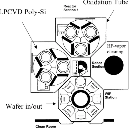
In order to increase the current driving capability and the transconductance of MOSFETs, the thickness of gate oxide must be scaled aggressively. However, as oxide thickness is reduced, oxide integrity becomes an important issue due to the increased direct-tunneling current density and applied electric field. Both intrinsic traps and soft breakdown are observed in ultrathin oxides [1]. Intrinsic traps increase leakage current [2] and soft breakdown limits device reliability [3]. The key issues for the thin oxide are thickness uniformity and interface smoothness [4]. The interface roughness can strongly affect the carrier transport. Unfortunately, the presence of native oxide causes the rough interface and degrades oxide reliability. In addition, as the oxide thickness is scaled down, the ratio of native oxide to total oxide becomes large. Therefore, the removal of the native oxide prior to gate oxidation becomes necessary for thin oxide. The native oxide thickness can reach 5-10Å within 10 minutes in the laboratory ambient. It has been reported in-situ HF-vapor pre-oxidation treatment can effectively strip native oxide by an advance clustered vertical furnace [5]. Gate oxide integrity can be significantly improved in terms of leakage, time-to-breakdown, breakdown field, interface-state-density, stress-induced leakage current, transconductance and driving current with in-situ HF-vapor cleaning [6]. Figure 1-1 shows
the top view of clustered vertical system (ASM-A400) consisting of three modules (HF-vapor cleaning, oxidation, poly-Si deposition). Wafers were processed through these three modules in sequence without exposure to the ambient. Since nMOSFETs performance is significantly improved with HF-vapor treatment [7], we investigated HF-vapor pre-oxidation cleaning for pMOSFETs in this study.
1-2 Hi-Wafer
CZ (Czochralski grown) wafer includes supersaturated oxygen atoms for oxygen precipitation, which are introduced during crystal growth. The oxygen induces many micro defects during heat process [8]. The microdefects, which are induced near surface area, cause various harmful defects such as OSF (Oxidation induced Stacking Fault), pattern edge dislocations, gate oxide breakdown failures and so on. Therefore, we need wafers which have to be free of defects in the device active layer and adequate oxygen precipitates in the bulk region to enable intrinsic gettering for metallic contamination [9]. It has been reported that such wafers can be produced by hydrogen annealing at high temperatures [10-12]. Hydrogen annealed wafers (Hi-wafer) have less oxygen defects than CZ wafers. A high temperature annealing in hydrogen ambient has high efficiency to eject the oxygen atoms
from the surface area. Figure 1-2 shows the oxygen out diffusion profile after annealing in hydrogen or oxygen ambient [8]. It was also reported that nMOSFETs fabricated on Hi-wafer show significant electrical improvement and have reduced donor-like interface trapping densities [13]. However, pMOSFETs on Hi-wafer have not been studied. In this study, we investigated the pMOSFETs fabricated on Hi-wafer.
1-3 Boron Penetration
The p+ poly gate is typically fabricated in a CMOS technology by implanting either B or BF2 into intrinsic polysilicon with subsequent RTA.Boron penetration through thin oxide
is a serious problem as the gate oxide thickness of MOSFETs scales toward 2-nm and below [14]. Various techniques have been proposed to reduce boron penetration through thin gate oxide. Oxynitride has good resistance to boron penetration [15] [16]. The reduction of fluorine incorporation during gate doping is also effective in reducing boron diffusion through the gate oxide [17]. It has been reported that amorphous-silicon film crystallized at 1000°C has the stacked grain structure due to high nucleation rate [18] [19], while the as deposited poly-Si film has the columnar grain structure [20]. The columnar grain structure in as-deposited poly-Si film enhances the dopant diffusion along the grain boundaries while
the stacked grain structure in crystallized α-Si film slows down boron diffusion in the gate [21]. Therefore, we also use the stack gate (α-Si 500Å + poly-Si 1500Å) to compare with conventional poly-Si gate in this study.
1-4 Thesis Organization
This thesis is divided into four chapters as follows:
In chapter 1, general backgrounds of HF-vapor treatment, hydrogen annealed wafer (Hi-wafer), boron penetration are introduced. The organization throughout this dissertation is described here.
In chapter 2, we illustrate the process flow for fabricating p-channel metal oxide semiconductor field effect transistors.
In chapter 3, we demonstrate the characteristics of pMOSFETs with HF-vapor pre-oxidation cleaning on different Si substrates. We also compare pMOSFETs on CZ wafer and Hi wafer. At last, the comparison of stack gate (α-Si 500Å + poly-Si 1500Å) and poly-gate is discussed.
Fig. 1-1 Advanced cluster system: vertical furnace with in-situ HF-Vapor cleaning. Wafers can be processed through these modules in sequence without exposure to the ambient, so as to obtain native-oxide-free MOS capacitors.
Fig.1-2 Oxygen depth profile after anneal at 1200℃ for 1 hour. [ Ref. Y. Matsushita, S.Samata, M.Miyashita and H.Kubota, “Improvement of Thin Oxide Quality by Hydrogen Annealed Wafer,” Tech. Dig. Int. Electron Devices Meet., pp. 321, 1994. ]
Chapter 2
Device fabrication
P-channel MOSFETs were fabricated on 6-in p-type Czochralski-grown (CZ) and Hydrogen-annealed (Hi) silicon wafers with a resistivity of 15-20Ω-cm by a conventional pMOSFETs process. An As+ implantation (E: 120 keV, D: 3×1012 cm-2) was used for the channel stop. Local oxidation of silicon (LOCOS) was used for device isolation. An As+ channel implantation (E: 80 keV, D: 1×1013 cm-2 ) was used for the adjustment of the threshold voltage. Anti-punch-through implantation was also performed to prevent bulk punch-through by phosphorus at 120 keV to a dose of 4×10¹²
cm-2. Before the gate dielectric growth, in-situ HF vapor clean was used to remove native oxide effectively in addition to traditional RCA clean. Then a gate oxide with a thickness of 2-nm was grown in either O2
or N2O ambient by a vertical furnace. Traditional poly-Si gate (200-nm) or stack gate (α-Si
50-nm + poly-Si 150-nm) was deposited in the vertical furnace followed by gate oxidation. Then, poly-Si gate and stack gate were patterned. After sidewall polymer removal, reoxidation is used to improve the oxide quality of the gate edge. Shallow S/D extensions were formed by BF2 implantation at 8 keV to a dose of 1×1015 cm-2. After the formation of a
TEOS sidewall spacer (200-nm), deep source/drain junctions were formed by BF2
implantation at 15 keV to a dose of 5×1015 cm-2. Then a 550-nm TEOS layer was deposited and etched for contact holes. A Ti/TiN/Al-Si-Cu/TiN 4-layer metal was deposited and
patterned to complete contact metallization. Finally, annealing in a H2 / N2 ambient at 400℃
Process Flow Diagram
O2 Oxide, N2O Oxide 2-nm
Well formation
LOCOS formation
Eliminate Kooi effect
Spacer formation
Gate oxide formation
Gate patterning
Poly-Si deposition
N-well P+: E:120keV D:1×1013 cm-2 SiO2 550-nm Poly-Si orα-Si+poly-Si : 200-nm BF2 : E: 15keV D: 5×1015cm-2S/D extension implant
BF2 : E: 8keV D: 1×1015 cm-2Source/Drain implant
Substrate implant
As : E: 40keV D: 5×10¹⁵
Contact hole
Ti/TiN/Al/TiN
TEOS deposition
Activation
Metal
Sintering
RTA : 1000℃, 10s TEOS 550-nm H2 : 400℃, 30minSchematic cross-section of device process flow
z LOCOS formation
1. Oxide 35-nm
2. Nitride 150-nm
3. Define active region
4. Channel stop implantation
5. Field oxide 550-nm
6. Remove nitride
z p-type Si wafer
z Well formation
1. N-well implantation
2. Well drive-in (1100℃, 170-nm)
z Gate
1. HF vaper cleaning
2. Gate oxide: 2.0-nm (N
2O or Dry O
2)
3. Gate: poly-Si or α-Si+poly-Si
z S/D extension implantation
P-substrate N-well P+ P+ FOX FOX P P N+ N+ Poly-Si α-Si TEOS TEOS P-substrate N-well P+ P+ FOX FOX P P N+ N+ Poly-Si α-Si TEOS TEOS
Fig.2-2 Schematic cross-section of device process flow.
z Spacer formation
1. TEOS 200-nm
2. Spacer etching
z S/D implantation
( S:BF
2E:15keV D:5×10
15cm
-2)
z TEOS deposition 550-nm
z Contact hole
1. Contact alignment
2. Contact etching
z Metal
1. Ti/TiN/Al-Si-Cu/TiN
2. Metal alignment
3. Metal etching
z Sintering
( 400℃, 30min )
Chapter 3
Results and Discussion
3-1 HF-vapor cleaning on different silicon substrate
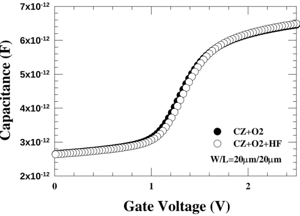
In-situ HF-vapor cleaning has been reported to improve nMOSFETs performance in terms of leakage, time-to-breakdown, breakdown field, interface-state-density, Id and gm [5]. In this study, we used HF-vapor cleaning for pMOSFETs on CZ-wafer and Hi-wafer with O2 or N2O oxide. Figure 3-1-1 shows the C-V characteristics for the samples with and
without HF-vapor cleaning on CZ-wafer with O2 oxide. It shows that HF-vapor cleaning
does not change the C-V curve. The oxide thickness calculated from the capacitance at accumulation region is about 2.1-nm. The hole mobility for the samples with and without HF-vapor cleaning on CZ-wafer with O2 oxide are shown in Fig. 3-1-2. The mobility for
HF-vapor cleaning sample is slightly large than the sample without HF-vapor cleaning. Figure 3-1-3 shows Id-Vd characteristics for the samples with and without HF-vapor cleaning on CZ-wafer with O2 oxide. HF-vapor cleaning increases the drain current in
CZ-wafer with O2 oxide. Figure 3-1-4 shows the charge pumping current for the samples
with and without HF-vapor cleaning on CZ-wafer with O2 oxide. The sample with
HF-vapor cleaning has reduced charge pumping current. It means that HF-vapor cleaning improves SiO2/Si interface quality as the gate dielectric is grown in O2 ambient. Figure
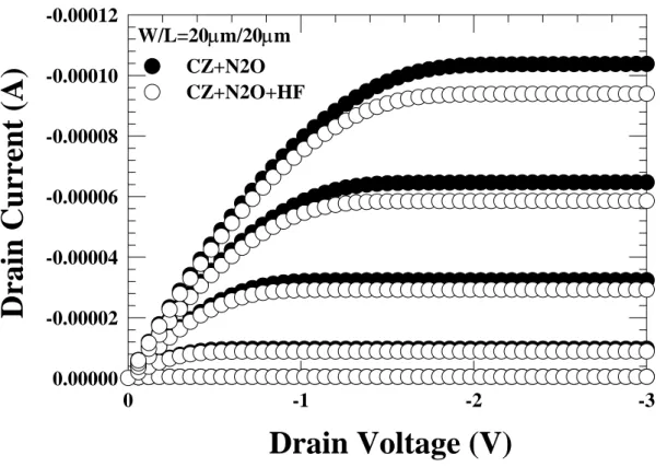
with N2O oxide. We found that HF-vapor cleaning degrades mobility with N2O oxide on
CZ-wafer. However, the Vt of the sample with HF-vapor cleaning is larger than that without HF-vapor cleaning. This means boron penetration for the sample without HF-vapor cleaning is more serious than HF-vapor cleaning sample. Therefore, The difference of mobility between two samples is determined by buried channel level. Figure 3-1-6 shows the Id-Vd characteristics for the samples with and without HF-vapor cleaning on CZ-wafer with N2O
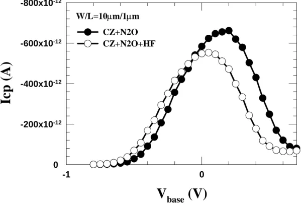
oxide. The devices with HF-vapor cleaning show the smaller drain current due to the smaller mobility. Figure 3-1-7 shows the charge pumping current for the sample with and without HF-vapor cleaning on CZ-wafer with N2O oxide. The sample without HF-vapor
cleaning presents larger charge pumping current than that with HF-vapor cleaning. It is consistent with the difference of Vt. The sample with smaller Vt suffer more serious boron penetration has larger charge pumping current. Figure 3-1-8 shows the hole mobility for the samples with and without HF-vapor cleaning on Hi-wafer with O2 oxide. There is no
difference between two samples. The HF-vapor cleaning didn’t improve the mobility for Hi-wafer with O2 oxide. Figure 3-1-9 shows the Id-Vd characteristics for the samples with
and without HF-vapor cleaning on Hi-wafer with O2 oxide. The result is consistent with the
mobility characteristics. The drain current of two samples are almost the same. Figure 3-1-10 shows the charge pumping current for the sample with and without HF-vapor cleaning on Hi-wafer with O2 oxide. HF-vapor cleaning didn’t improve the interface quality
on Hi-wafer with O2 oxide. Figure 3-1-11 shows the hole mobility for the samples with and
without HF-vapor cleaning on Hi-wafer with O2 oxide. The HF-vapor cleaning sample
shows larger hole mobility. However, this is just caused by the different levels of buried channel. The HF-vapor cleaning sample that has smaller Vt is consistent with its larger mobility. The HF-vapor cleaning sample has larger drain current as shown in Fig. 3-1-12. Figure 3-1-13 shows the charge pumping current for the sample with and without HF-vapor cleaning on Hi-wafer with N2O oxide. The HF-vapor cleaning sample shows larger charge
pumping current. It demonstrates that HF-vapor cleaning sample with smaller Vt suffers more serious boron penetration as we reported above.
W/L=20µm/20µm
Gate Voltage (V)
0 1 2Capacitance (F)
2x10-12 3x10-12 4x10-12 5x10-12 6x10-12 7x10-12 CZ+O2 CZ+O2+HFFig. 3-1-1 C-V characteristics of pMOSFETs with HF-vapor treatment and without HF-vapor treatment on CZ-wafer with O2 oxide.
W/L=50µm/50µm
Vg-Vt (V)
-1 0Mobility (cm
2
/V-sec)
0 20 40 60 80 CZ+O2 CZ+O2+HFFig. 3-1-2 Hole mobility of pMOSFETs with HF-vapor treatment and without HF-vapor treatment on CZ-wafer with O2 oxide.
W/L=20µm/20µm
Drain Voltage (V)
-3 -2 -1 0Drain Current (A)
-0.00012 -0.00010 -0.00008 -0.00006 -0.00004 -0.00002 0.00000 CZ+O2 CZ+O2+HF
Fig. 3-1-3 Id-Vd characteristics of pMOSFETs with HF-vapor treatment and without HF-vapor treatment on CZ-wafer with O2 oxide.
W/L=10µm/1µm
V
base(V)
0 1Icp (A)
-800x10-12 -600x10-12 -400x10-12 -200x10-12 0 CZ+O2 CZ+O2+HFFig. 3-1-4 Charge pumping current for pMOSFETs with HF-vapor treatment and without HF-vapor treatment on CZ-wafer with O2 oxide (1MHZ).
W/L=50µm/50µm
Vg-Vt (V)
-1 0Mobility (cm
2
/V-sec)
0 20 40 60 80 CZ+N2O CZ+N2O+HFFig. 3-1-5 Hole mobility of pMOSFETs with HF-vapor treatment and without HF-vapor treatment on CZ-wafer with N2Ooxide.
W/L=20µm/20µm
Drain Voltage (V)
-3 -2 -1 0Drain Current (A)
-0.00012 -0.00010 -0.00008 -0.00006 -0.00004 -0.00002 0.00000 CZ+N2O CZ+N2O+HF
Fig. 3-1-6 Id-Vd characteristics of pMOSFETs with HF-vapor treatment and without HF-vapor treatment on CZ-wafer with N2O oxide.
W/L=10µm/1µm
V
base(V)
-1 0Icp (A)
-800x10-12 -600x10-12 -400x10-12 -200x10-12 0 CZ+N2O CZ+N2O+HFFig. 3-1-7 Charge pumping current for pMOSFETs with HF-vapor treatment and without HF-vapor treatment on CZ-wafer with O2 oxide (1MHZ).
W/L=50µm/50µm
Vg-Vt (V)
-1 0Mobility (cm
2
/V-sec)
0 20 40 60 80 HI+O2 HI+O2+HFFig. 3-1-8 Hole mobility of pMOSFETs with HF-vapor treatment and without HF-vapor treatment on Hi-wafer with O2 oxide.
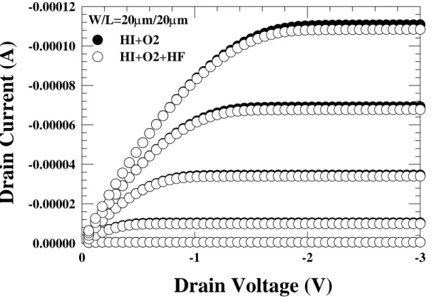
W/L=20µm/20µm
Drain Voltage (V)
-3 -2 -1 0Drain Current (A)
-0.00012 -0.00010 -0.00008 -0.00006 -0.00004 -0.00002 0.00000 HI+O2 HI+O2+HF
Fig. 3-1-9 Id-Vd characteristics of pMOSFETs with HF-vapor treatment and without HF-vapor treatment on Hi-wafer with O2 oxide.
W/L=10µm/1µm
V
base(V)
-1 0Icp (A)
-800x10-12 -600x10-12 -400x10-12 -200x10-12 0 HI+O2 HI+O2+HFFig. 3-1-10 Charge pumping current for pMOSFETs with HF-vapor treatment and without HF-vapor treatment on Hi-wafer with O2 oxide (1MHZ).
W/L=50um/50um
Vg-Vt (V)
-1 0Mobility (cm
2
/V-sec)
0 20 40 60 80 HI+N2O HI+N2O+HFFig. 3-1-11 Hole mobility of pMOSFETs with HF-vapor treatment and without HF-vapor treatment on Hi-wafer with N2O oxide.
W/L=20µm/20µm
Drain Voltage (V)
-3 -2 -1 0Drain Current (A)
-0.00012 -0.00010 -0.00008 -0.00006 -0.00004 -0.00002 0.00000 HI+N2O HI+N2O+HF
Fig. 3-1-12 Id-Vd characteristics of pMOSFETs with HF-vapor treatment and without HF-vapor treatment on Hi-wafer with O2 oxide.
W/L=10µm/1µm
V
base(V)
-1 0Icp (A)
-800x10-12 -600x10-12 -400x10-12 -200x10-12 0 HI+N2O HI+N2O+HFFig. 3-1-13 Charge pumping current for pMOSFETs with HF-vapor treatment and without HF-vapor treatment on Hi-wafer with N2Ooxide (1MHZ).
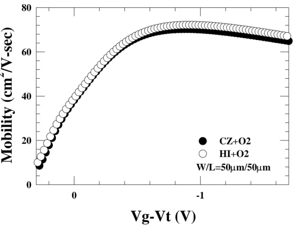
3-2 Comparison of CZ-wafer and Hi-wafer
Gate oxide integrity is strongly dependent on both contamination during oxidation process and silicon wafer surface quality. The contamination can be minimized by controlling the cleaning process, gas purity, oxidation environment and so on. However, it is difficult to improve the wafer surface quality during the oxidation process. The wafer quality is determined by both impurities in the crystal and thermal history during crystal growth. It is reported that high temperature annealing in hydrogen can eject the oxygen atoms from the surface area and improve the wafer surface quality [8]. It is also reported nMOSFETs fabricated on Hi-wafer show significant electrical improvement and have reduced donor-like interface trapping densities [13]. In this study, we investigated the pMOSFETs fabricated on Hi-wafer. Figure 3-2-1 shows hole mobility for CZ-wafer and Hi-wafer with O2 oxide. The mobility for Hi-wafer is slightly larger than CZ-wafer. Charge
pumping current for Hi-wafer is smaller than CZ-wafer as shown in Fig. 3-2-2. This result indicates Hi-wafer has less interface-state-density than CZ-wafer with O2 oxide. Hi-wafer
indeed shows better interface quality. Figure 3-2-3 shows the Id-Vd characteristics for CZ-wafer and Hi-wafer with O2 oxide. Hi-wafer shows larger drain current than CZ-wafer.
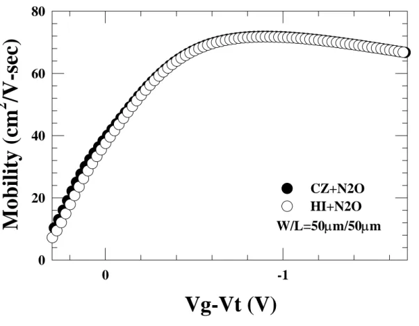
Figure 3-2-4 shows hole mobility for CZ-wafer and Hi-wafer with N2O oxide. The result is
different from the O2 oxide. There is no improvement for Hi-wafer with N2O oxide.
shown in Fig. 3-2-5. Figure 3-2-6 shows the Id-Vd characteristics for CZ-wafer and Hi-wafer with N2O oxide. We found that Hi-wafer shows no improvement for drain current with N2O oxide. It is reported that nitrogen incorporation causes the shallow donor-like
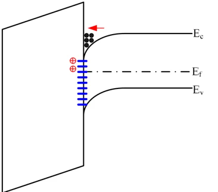
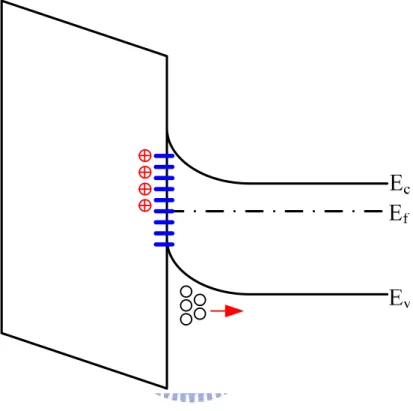
traps that exist at the interface of oxynitride and silicon substrate [22][23]. It is also reported that Hi-wafer has reduced donor-like interface trapping densities due to the less oxygen atoms [13]. The donor-like traps with positive charges may attract the electrons to surface for nMOSFETs as shown in Fig. 3-2-7. Therefore, the reduction of donor-like interface trapping densities can enhance the mobility of nMOSFETs due to less surface scattering. Figure 3-2-8 shows the band diagram of pMOSFET. The donor-like traps with positive charges may repel the holes from interface and holes can move with less surface scattering for pMOSFETs. Therefore, the reduction of donor-like interface trapping densities doesn’t enhance the mobility of pMOSFETs.
W/L=50µm/50µm
Vg-Vt (V)
-1 0Mobility (cm
2
/V-sec)
0 20 40 60 80 CZ+O2 HI+O2W/L=10µm/1µm
V
base(V)
0 1Icp (A)
-800x10-12 -600x10-12 -400x10-12 -200x10-12 0 CZ+O2 HI+O2Fig. 3-2-2 Charge pumping current for CZ-wafer and Hi-wafer with O2 oxide (1MHZ).
W/L=20µm/20µm
Drain Voltage (V)
-3 -2 -1 0Drain Current (A)
-0.00012 -0.00010 -0.00008 -0.00006 -0.00004 -0.00002 0.00000 CZ+O2 HI+O2
W/L=50µm/50µm
Vg-Vt (V)
-1 0Mobility (cm
2
/V-sec)
0 20 40 60 80 CZ+N2O HI+N2OW/L=10µm/1µm
V
base(V)
0 1Icp (A)
-800x10-12 -600x10-12 -400x10-12 -200x10-12 0 CZ+N2O HI+N2OFig. 3-2-5 Charge pumping current for CZ-wafer and Hi-wafer with N2O oxide (1MHZ).
W/L=20µm/20µm
Drain Voltage (V)
-3 -2 -1 0Drain Current (A)
-0.00012 -0.00010 -0.00008 -0.00006 -0.00004 -0.00002 0.00000 CZ+N2O HI+N2O
3-3 Comparison of stack gate and poly gate
P+ poly gate is essentially when pMOSFETs are scaled down to the deep submicrometer regime. However, the penetration of Boron impurity from the p+ poly through the gate oxide into the channel region is a critical issue. In this study, we fabricated the pMOSFETs with stack gate (α-Si 500Å + poly-Si 1500Å) and conventional poly-gate (poly-Si 2000Å) to investigate the boron penetration. The C-V characteristics for stack gate and poly gate on CZ-wafer with O2 oxide are shown in Fig. 3-3-1. The slope of C-V curve
of poly-gate is steeper than that of stack gate. This result implies that the pMOSFETs with poly-gate have become buried-channel devices. A very shallow, fully-depleted p-type layer exists in the silicon substrate close to the SiO2/Si interface due to serious boron penetration
and insufficient threshold voltage adjustment implantation. The existence of p-type layer can make the inversion of holes easier for pMOSFETs as shown in Fig. 3-3-2. However, stack gate pMOSFETs are still surface channel devices and present the resistance of boron penetration. Figure 3-3-3 shows the hole mobility of stack gate and poly gate on CZ-wafer with O2 oxide. The hole mobility of poly gate is larger than stack gate. The larger mobility
of poly gate is due to the buried channel. Carriers transport in the buried channel with less surface scattering than in surface channel. Furthermore, It is reported that this kind of stack gate (α-Si + poly-Si ) causes tensile strain in the channel region and enhance electron mobility [22]. However, the tensile strain degrades hole mobility for pMOSFETs. Therefore,
the smaller mobility of stack gate is result from both surface channel and tensile strain. The Id-Vd characteristics of stack gate and poly gate on CZ-wafer with O2 oxide are shown in
Fig. 3-3-4. The drain current of stack gate is much smaller than poly gate due to smaller hole mobility. Figure 3-3-5 and figure 3-3-6 illustrate the mobility and Id-Vd characteristics of stack gate and poly gate on CZ-wafer with N2O oxide. The pMOSFETs with poly gate
present larger mobility and drain current than stack gate due to the reasons we discussed before. Figure 3-3-7 ~ 3-3-9 show the C-V, mobility and Id-Vd characteristics of stack gate and poly gate on Hi-wafer with O2 oxide. Figure 3-3-10 and figure 3-3-11 show the mobility
and Id-Vd characteristics of stack gate and poly gate on Hi-wafer with N2O oxide. All
results show that pMOSFETs with stack gate are still surface channel devices with less boron penetration whereas pMOSFETs with poly gate become buried channel devices due to serious boron penetration. The sheet resistance of stack gate and poly gate on CZ-wafer and on Hi-wafer are shown in Fig. 3-3-12 and Fig. 3-3-13 respectively. The sheet resistance of poly gate is larger than stack gate no matter on CZ-wafer or on Hi-wafer. This means that there are more dopant in stack gate than in poly gate due to less boron penetration. Figure 3-3-14 and Figure 3-3-15 illustrate the charge pumping current of stack gate and poly gate with O2 oxide on CZ-wafer and Hi-wafer respectively. The charge pumping current of stack
gate is much smaller than poly gate no matter on CZ-wafer or Hi-wafer. This indicates that the interface quality of stack gate is better than poly gate. Boron penetration through gate
oxide will damage the oxide and the SiO2/Si interface. Therefore, the better interface quality
means that the oxides of stack gate pMOSFETs suffer less boron penetration. Figure 3-3-16 and Figure 3-3-17 show Ig-Vg characteristics of stack gate and poly gate with O2 oxide on
CZ-wafer and Hi-wafer respectively. There is a hump at low positive voltage for poly gate whereas stack gate doesn’t have. It may be due to interface states assisted tunneling. The oxides of poly gate pMOSFETs suffer more serious boron penetration and have more interface traps than stack gate due to oxide damage. Electron can tunnel through oxide easily by these traps. Figure 3-3-18 shows the transconductance versus gate length for stack gate and poly gate with O2 oxide on CZ wafer. We can observe that the transconductance of
poly gate is larger than stack gate as the gate length is above 1.5µm and the opposite result as the gate length is under 1.5µm. The same results are found on CZ-wafer and Hi-wafer with O2 oxide and N2O oxide as shown in Fig. 3-3-19 ~ Fig. 3-3-21. Figure 3-3-22 shows
gm × W/L versus gate length for stack gate and poly gate with O2 oxide on CZ-wafer. The
decrease of gm × W/L for poly gate is severer than stack gate as the gate length scales down. The same results are found on CZ-wafer and Hi-wafer with O2 oxide and N2O oxide as
shown in Fig. 3-3-23 ~ Fig. 3-3-25. The severe decrease of gm × W/L indicates that short-channel-effect of poly gate is serious due to the buried channel. However, the pMOSFETs with stack gate show the superior short channel characteristics. Figure 3-3-26 shows Id-Vg characteristics for stack gate and poly gate on CZ-wafer with O2 oxide. It is
obvious that device with poly gate shows larger off-current than stack gate due to buried channel. Figure 3-3-27 shows the threshold voltage versus device location on CZ-wafer with O2 oxide. Figure 3-3-28 indicates that the Vt difference between poly and stack gate is
not caused by gate oxide thickness. It indicates that the threshold voltage variation of devices with stack gate is less than poly gate. All of the results demonstrate that pMOSFETs with stack gate can effectively suppress boron penetration. It may be due to that amorphous-silicon film crystallized at 1000°C has the stacked grain structure due to high nucleation rate [18] [19], while the as deposited poly-Si film has the columnar grain structure [20]. The columnar grain structure in as-deposited poly-Si film enhances the dopant diffusion along the grain boundaries while the stacked grain structure in crystallized α-Si film can slow down boron diffusion in the gate [21].
W/L=20µm/20µm
Gate Voltage (V)
0 1 2Capacitance (F)
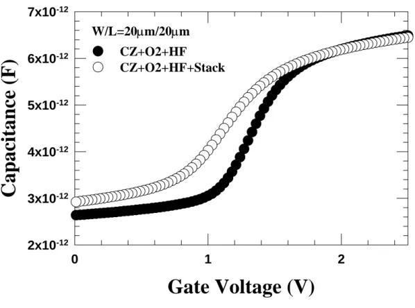
2x10-12 3x10-12 4x10-12 5x10-12 6x10-12 7x10-12 CZ+O2+HF CZ+O2+HF+StackFig. 3-3-1 C-V characteristics for stack-gate and poly-gate on CZ-wafer with O2
E
cE
vE
fW/L=50µm/50µm
Gate Voltage (V)
-2 -1 0Mobility (cm
2
/V-sec)
0 20 40 60 80 CZ+O2+HF CZ+O2+HF+StackFig. 3-3-3 Hole mobility for stack-gate and poly-gate on CZ-wafer with O2
W/L=20µm/20µm
Drain Voltage (V)
-3 -2 -1 0Drain Current (A)
-0.00012 -0.00010 -0.00008 -0.00006 -0.00004 -0.00002 0.00000 CZ+O2+HF+Stack CZ+O2+HF
Fig. 3-3-4 Id-Vd characteristics for stack-gate and poly-gate on CZ-wafer with O2 oxide.
W/L=50µm/50µm
Gate Voltage (V)
-2 -1 0Mobility (cm
2
/V-sec)
0 20 40 60 80 CZ+N2O+HF CZ+N2O+HF+StackFig. 3-3-5 Hole mobility for stack-gate and poly-gate on CZ-wafer with N2O
W/L=20µm/20µm
Drain Voltage (V)
-3 -2 -1 0Drain Current (A)
-0.00012 -0.00010 -0.00008 -0.00006 -0.00004 -0.00002 0.00000 CZ+N2O+HF+Stack CZ+N2O+HF
Fig. 3-3-6 Id-Vd characteristics for stack-gate and poly-gate on CZ-wafer with N2O oxide.
W/L=20µm/20µm
Gate Voltage (V)
0 1 2Capacitance (F)
2x10-12 3x10-12 4x10-12 5x10-12 6x10-12 7x10-12 HI+O2+HF HI+O2+HF+StackFig. 3-3-7 C-V characteristics for stack-gate and poly-gate on Hi-wafer for O2
W/L=50µm/50µm
Gate Voltage (V)
-2 -1 0Mobility (cm
2
/V-sec)
0 20 40 60 80 HI+O2+HF HI+O2+HF+StackW/L=20µm/20µm
Drain Voltage (V)
-3 -2 -1 0Drain Current (A)
-0.00012 -0.00010 -0.00008 -0.00006 -0.00004 -0.00002 0.00000 HI+O2+HF+Stack HI+O2+HF
Fig. 3-3-9 Id-Vd characteristics for stack-gate and poly-gate on Hi-wafer with O2 oxide.
W/L=50µm/50µm
Gate Voltage (V)
-2 -1 0Mobility (cm
2
/V-sec)
0 20 40 60 80 HI+N2O+HF HI+N2O+HF+StackFig. 3-3-10 Hole mobility for stack-gate and poly-gate on Hi-wafer with N2O
W/L=20µm/20µm
Drain Voltage (V)
-3 -2 -1 0Drain Current (A)
-0.00012 -0.00010 -0.00008 -0.00006 -0.00004 -0.00002 0.00000 HI+N2O+HF+Stack HI+N2O+HF
Fig. 3-3-11 Id-Vd characteristics for stack-gate and poly-gate on Hi-wafer with N2O oxide.
Split
CZ+OCZ+O2+HF2+HF+StackCZ+N2O+H
F CZ+N2O+H F+Stack
Sheet Resistance (
Ω
/sq)
1600 1800 2000 2200 2400 2600 2800Split
HI+O2+HF HI+O2+HF+S tack HI+N2O+HF HI+N2O+HF +StackSheet Resistance (
Ω
/sq)
2000 2200 2400 2600 2800 3000 3200 3400 3600W/L=10µm/1µm
V
base(V)
-1 0 1Icp (A)
-600x10-12 -500x10-12 -400x10-12 -300x10-12 -200x10-12 -100x10-12 0 CZ+O2+HF CZ+O2+HF+StackFig. 3-3-14 Charge pumping current for stack-gate and poly-gate on CZ-wafer with O2 oxide (1MHZ).
W/L=10µm/1µm
V
base(V)
-1 0 1Icp (A)
-600x10-12 -500x10-12 -400x10-12 -300x10-12 -200x10-12 -100x10-12 0 HI+O2+HF HI+O2+HF+StackFig. 3-3-15 Charge pumping current for stack-gate and poly-gate on Hi-wafer with O2 oxide (1MHZ).
W/L=20µm/20µm
Gate Voltage (V)
-3 -2 -1 0 1 2 3Ig
1x10-15 10x10-15 100x10-15 1x10-12 10x10-12 100x10-12 1x10⁻⁹ 10x10-9 100x10-9 1x10⁻⁶ 10x10-6 CZ+O2+HF CZ+O2+HF+StackFig. 3-3-16 Gate current versus gate voltage for stack-gate and poly-gate on CZ-wafer with O2 oxide.
W/L=20µm/20µm
Gate Voltage (V)
-3 -2 -1 0 1 2 3Ig
1x10-15 10x10-15 100x10-15 1x10-12 10x10-12 100x10-12 1x10⁻⁹ 10x10-9 100x10-9 1x10⁻⁶ 10x10-6 HI+O2+HF HI+O2+HF+StackFig. 3-3-17 Gate current versus gate voltage for stack-gate and poly-gate on Hi-wafer with O2 oxide.
Gate Length
(
µm)
0 1 2 3 4 5Gm (
µS)
20 40 60 80 100 120 140 160 180 CZ+O2+HF CZ+O2+HF+StackFig. 3-3-18 Gm versus gate length for stack-gate and poly-gate on CZ-wafer with O2 oxide.
Gate Length (
µm)
0 1 2 3 4 5Gm (
µS)
20 40 60 80 100 120 140 160 180 CZ+N2O+HF CZ+N2O+HF+StackFig. 3-3-19 Gm versus gate length for stack-gate and poly-gate on CZ-wafer with N2O oxide.
Gate Length
(
µm)
0 1 2 3 4 5Gm (
µS)
20 40 60 80 100 120 140 160 180 HI+O2+HF HI+O2+HF+StackFig. 3-3-20 Gm versus gate length for stack-gate and poly-gate on Hi-wafer with O2 oxide.
Gate Length (
µm)
0 1 2 3 4 5Gm (
µS)
20 40 60 80 100 120 140 160 180 HI+N2O+HF HI+N2O+HF+StackFig. 3-3-21 Gm versus gate length for stack-gate and poly-gate on Hi-wafer with N2O oxide.
Gate Length
(
µm)
0
1
2
3
4
5
Gm x L/W (
µS)
3
4
5
6
7
CZ+O2+HF
CZ+O2+HF+Stack
Fig. 3-3-22 Gm × L/W versus gate length for stack-gate and poly-gate on CZ-wafer with O2 oxide.
Gate Length (
µm)
0
1
2
3
4
5
Gm x L/W (
µS)
3
4
5
6
7
CZ+N2O+HF
CZ+N2O+HF+Stack
Fig. 3-3-23 Gm × L/W versus gate length for stack-gate and poly-gate on CZ-wafer with N2O oxide.
Gate Length
(
µm)
0
1
2
3
4
5
Gm x L/W (
µS)
3
4
5
6
7
HI+O2+HF
HI+O2+HF+Stack
Fig. 3-3-24 Gm × L/W versus gate length for stack-gate and poly-gate on Hi-wafer with O2 oxide.
Gate Length (
µm)
0
1
2
3
4
5
Gm x L/W (
µS)
3
4
5
6
7
HI+N2O+HF
HI+N2O+HF+Stack
Fig. 3-3-25 Gm × L/W versus gate length for stack-gate and poly-gate on Hi-wafer with N2O oxide.
W/L=20µm/20µm
Gate Voltage (V)
-2 -1 0 1Drain Current (A)
10-13 10-12 10-11 10-10 10-9 10-8 10-7 10-6 10-5 10-4 10-3 CZ+O2+HF CZ+O2+HF+Stack
Fig. 3-3-26 Id-Vg characteristics for stack gate and poly gate on CZ-wafer with O2 oxide.
W/L=20µm/20µm
Position from Center (cm)
-6 -4 -2 0 2 4
Vth (mV)
-600 -500 -400 -300 -200 -100 0 100 200 300 400 500 600 700 CZ+O2+HF CZ+O2+HF+StackFig. 3-3-27 Vth versus device location for stack gate and poly gate on CZ-wafer with O2 oxide.
W/L=20
µm/20µm
Position from Center (cm)
-6
-4
-2
0
2
4
Capacitance (F)
6.0x10
-126.1x10
-126.2x10
-126.3x10
-126.4x10
-126.5x10
-126.6x10
-126.7x10
-126.8x10
-12CZ+O2+HF
CZ+O2+HF+Stack
Fig. 3-3-28 Cox versus device location for stack gate and poly gate on CZ-wafer
Chapter 4
Summary and Conclusion
In-situ HF-vapor cleaning on CZ-wafer with O2 oxide can improve interface quality
and enhance the mobility and drain current for pMOSFETs. However, HF-vapor cleaning on Hi-wafer with O2 oxide shows no improvement. The pMOSFETs on Hi-wafer present lower
interface-state-densities than CZ-wafer. We found that pMOSFETs on Hi-wafer with O2
oxide exhibit improved performance in terms of mobility, drain current and interface-state-densities. However, there is no improvement on Hi-wafer with N2O oxide
due to reduced donor-like interface trapping densities. Finally, the pMOSFETs with stack gate (α-Si 500Å + poly-Si 1500Å) can effectively suppress boron penetration.
Reference
[1] J. M. Lai, W. H. Chieng, B. C. Lin, Albert Chin, and C. Tsai, “The Leakage Current Effect of Thin Gate Oxides with In Situ Native Oxide Desorption,” in Journal of The
Electrochemical Society, pp. 2216-2218, 1999.
[2] C. T. Lui, A. Ghetti, Y. Ma, G. P. Chng, K. P. PHeung, and J. T. Clemens, Tech. Dig. Int.
Electron Devices Meet., pp. 85, 1997.
[3] B. E. Weir, P. J. Silverman, D. Monroe, K. S. Krisch, M. A. Alam, G. B. Alers, Tech.
Dig. Int. Electron Devices Meet., pp. 73, 1997.
[4] Albert Chin, W. J. Chen, T. Chang, R. H. Kao, B. C. Lin, C. Tsai, and J. C. M. Huang, “ Thin Oxides with in situ Native Oxide Removal, ” IEEE Electron Device Letters, Vol. 18, NO. 9, pp. 417-419, 1997.
[5] T. S. Chao, J. L. Chen, C. S. Lai, H. C. Lin, and T. Y. Huang, “High Quality Ultra-Thin (2.4nm) Oxide Prepared by Clustered Vertical Furnace with In-situ HF-Vapor Pre-Gate Oxide Cleaning,“ VLSI Technology, pp. 74-77, June. 1999.
[6] Albert Chin, B. C. Lin, W. J. Chen, Y. B. Lin, and C. Tsai, “The Effect of Native Oxide on Thin Gate Oxide Integrity,” IEEE Electron Device Letters, Vol. 19, NO. 11, pp. 426-428, 1998.
[7] Jiann Heng Chen, Tan Fu Lei, Chia Lin Chen, Tien Sheng Chao, Wen Ying Wen, and Kuag Ting Chen. “High Performance Deep-Submicron n-MOSFETs by Nitrogen
Implantation and In-situ HF Vapor Clean,” International Reliability Physics
Symposium, pp. 180-185, 2000.
[8] Y. Matsushita, S.Samata, M.Miyashita and H.Kubota, “Improvement of Thin Oxide Quality by Hydrogen Annealed Wafer,” Tech. Dig. Int. Electron Devices Meet., pp. 321, 1994.
[9] Koji Izunome, Hiroshi Shirai, Kazuhiko Kashima, Jun Yoshikawa, and Akimichi Hojo, “Oxygen precipitation in Czochralski-grown silicon wafers During hydrogen
annealing,” Appl. Phys. Lett. pp.68, 1996.
[10] Y. Matsushita, M. Wakatuski, and Y. Saito, Extended Abstracts of the 18th Conference on Solid State Devices and Materials.
[11] S. Kurihara, Y. Kirino, Y. Matsushita, and K. Yamabe, Toshiba Rev. 49, pp. 387, 1994. [12] H. Tsuya, Oxygen in Silicon, edited by F. Shimura (Academic, Boston, 1994), pp. 661. [13] T. S. Chao, Y. H. Lin, and W. L. Yang “Mobility Enhancement of MOSFETs on
p-Silicon (111) With In situ HF-Vapor Pre-Gate Oxide Cleaning,” IEEE Electron
Device Letters, Vol. 25, NO.9, pp. 625-627, 2004.
[14] Min Cao, Paul Vande Voorde, Mike Cox, and Wayne Greene, “Boron Diffusion and Penetration with Poly-Si Gate,” IEEE Electron Device Letters, Vol. 19, NO.8, pp. 291-293, 1998.
oxynitride grown in nitric oxide (NO),” in Symp. VLSI Tech., pp. 105-106, 1994. [16] C. T. Liu, E. J. Lloyd, Y. Ma, M. Du, R. L. Opila, and S. J. Hillenius,
”High-performance 0.2-μm CMOS with 25Å gate oxide grown on nitrogen implanted Si substrates,” Tech. Dig. Int. Electron Devices Meet., pp. 499-503, 1996. [17] F. K. Baker, J. P. Pfiester, T. C. Mele, H-H. Tseng, P. J. Tobin, and J. D. Hayden,
“The influence of fluorine on the threshold voltage instabilities in p+ polysilicon
gated p-channel MOSFET’s,” Tech. Dig. Int. Electron Devices Meet., pp. 443-446, 1989.
[18] R. B. Iverson and R. Reif, “Recrystallization of amorphized polycrystalline silicon films on SiO2: Temperature dependence of the crystallization parameters,”
J. Appl. Phys., vol. 62, no. 5, pp. 1675-1681, 1987.
[19] N. G. Nakhodkin and T. V. Rodionova, “The mechanism of secondary grain growth in poly-silicon films,” J. Cryst. Growth, Vol. 171, pp. 50-55, 2000.
[20] T. Kamins, polycrystalline Silicon for Integrated Circuit Applications. Norwell, MA: Kluwer, ch. 2, 1988.
[21] Shye Lin Wu, Chung Len lee, and Tan Fu Lei, “Suppression of the Boron Penetration Induced Dielectric Degradation by Using a Stacked Amorphous Silicon Film as the Gate Structure for pMOSFET,” IEEE Trans. Electron Devices Lett, Vol. 43, NO. 2, pp.
[22] M. Suezawa, K. Sumino, H. Harada, and T. Abe, “Nitrogen-Oxygen Complexes as Shallow Donors in Silicon Crystals,” Jpn. J. of Applied Physic, 25, pp.L859-L861, 1986. [23] A. T. Wu, T. Y. Chan, V. Murali, S. W. Lee, J. Nulman, and M. Garner, “Nitridation Induced Surface Donor Layer in Silicon and Its Impact on the Characteristics of n- and p-Channel MOSFETS,” Tech. Dig. Int. Electron Devices Meet., pp. 271-274, 1989.