Light emission and detection
by
metal oxide silicon tunneling diodes
C. W. Liu,
M. H. Lee, C. F. Lin,
I. C.
Lin, W. T. Liu,
and
H. H. Lin
Department of Electrical Engineering, National Taiwan University, Taipei, TaiwanAbstract
Both NMOS and PMOS light-emitting diodes and photodetectors are demonstrated. For the ultrathin gate oxide, the tunneling gate of metal oxide silicon (MOS) diodes can be utilized as both emitters for light emitting devices and collectors for light detectors. An electron-hole plasma model is used to fit the emission spectra. A surface band bending is responsible for the bandgap reduction in electroluminescence (EL) from the MOS tunneling diode. The dark current of the photodetectors is limited by the thermal generation of minority carrier in the inversion layer. The high growth temperature(l000"C) of the oxide can reduce the dark current to a level as low as 3nAlcm2.
Introduction
It is a long sought goal to integrate ultra large scale integrated circuits(ULS1) with the electro-optics to possibly overcome the speed limitation of electrical interconnects and to reduce the complexity of the back-end process at the same time. Light emitting diodes and detectors are essential devices for this -application. An avalanche diode and a SiGe/Si p-i-n diode have been used as a light emitter to serve this purpose [1,2]. In this paper, a MOS tunneling diode biased at the accumulation region is used as a light emitting device and a MOS tunneling diode biased at the inversion region is used as a photodetector. Both are fully compatible with CMOS technology. The same device structure for emitters and detectors makes it possible to have a duplex mode of optical interconnects. On the other hand, the conventional CCD imager requires a serial readout and thus reduces readout speed. The tunneling gate current from the
MOS
diode biased in the inversion region can be used as a photo signal and can be read in parallel.Fabrication
The ultra thin gate oxide used in the study is grown by rapid thermal oxidation (RTO) at the 900-1000°C. The gas flows are 500 sccm nitrogen and 500 sccm oxygen at a reduced pressure. Before oxidation, the sample was cleaned by a HF dip and an in-situ hydrogen bake. After the growth of the ultra thin oxide, the sample was in-situ annealed in nitrogen for 10 min at 900°C. The thickness is measured by ellipsometer, confirmed by x-ray reflectivity and high frequency C-V measurements. The resistivities of the 100 mm p-type wafer and the lOOmm n-type wafer used in this
study are 1-5 and 1-10 ohm-cm, respectively. The MOS diodes had AI or indium tin oxide(IT0) gate electrodes with various circular areas defined by photolithography.
Light emitting diode
For NMOS diodes, the negative gate voltage will inject electrons from metal to silicon and attract the positive localized holes in the silicodoxide interface (accumulation layer). Fig. 1 shows the I-V curves of an A1/2.3nm oxide/p-Si device with oxide grown at 900 "C. Fig.2 plots the C-V curve of this NMOS diode. The diode area is 3x104 cm'. Using the equivalent circuit inserted in Fig.2, the thickness extracted from the C-V is about 2.6 nm, similar to the 2.3 nm measured by ellipsometer. The
FN
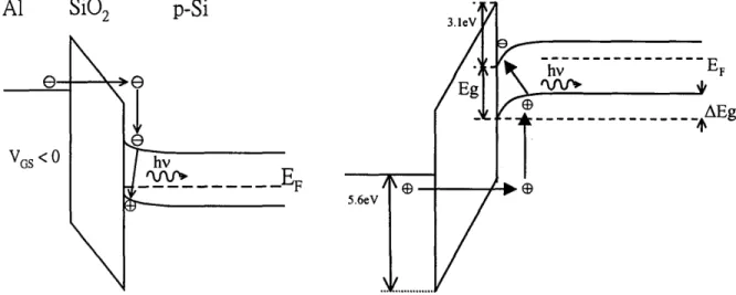
or direct tunneling current of electrons at the negative bias can cause electron hole recombination in the silicodoxide interface as shown in Fig.3. The interface roughness and spread in k-space due to localized holes in the accumulation layer can provide the extra momentum to emit the photons. Luminescence was clearly observed at the negative gate bias under continuous wave operation without cooling. Since the light was blocked by the thick AI gate electrode, only the emission from the diode edge was detected, as observed by IR viewer through a microscope. The photon emission spectra of a NMOS with a area of 4x10-' cm2 (Fig.4) have peaks at around 1.06 eV for gate voltage from negative 2.5 to 4 V, and the intensity increases as the voltage increases. Note that no light comes out from the diodes at positive gate bias.Fig.5 shows the typical I-V curves of a PMOS diode with the oxide thickness of 2.7 nm. When the A1 gate with the area of 3x104 cm2 was under positive bias, the electrons tunnel from the n-type silicon to the AI gate and the holes also tunnel from A1 gate to n-type silicon. As a result, a significant tunneling current was observed in the positive gate bias. However, due to the different barrier heights between electrons (-3.1 eV) and holes (-5.6eV), hole current may be smaller than the electron current (Fig.6). Meanwhile, the positive gate bias also attracts electrons in the silicodoxide interface to form an accumulation layer. Similarly, the localized electrons in the accumulation layer with localized wave functions and the Si/oxide interface roughness may provide extra momentum during the electron-hole radiative recombination. For the PMOS diode, intensive light (Fig.7) is also emitted by PMOS tunneling diode with a peak around 1.05 eV for gate bias from positive 3V to 5V. The emission intensity increases with the positive gate bias. The feature of the emission spectra is the asymmetrical broadening of the
31.3.1
emission peak, where the high-energy part is more broad than the low-energy part. This is very similar to the line shape of electron-hole-plasma (EHP) recombination. To confirm this observation, we fit the EL spectra by the line shape of EHP recombination [3]. Fig.7 also shows the theoretical EHP spectra, indicating an excellent fit to the experimental data. The bandgap obtained from the EHP model is about 1.01 eV to 1.03 eV for the gate voltage from 5V to 3V, lower than the Si bandgap of 1.12 eV at room temperature. This is unlikely due to high junction temperature in Si/oxide interface, since the temperature of 1.01 eV bandgap is about 600K and the EL spectra can not be fitted well using such high temperature. This reduction of bandgap can be understood by the surface band bending in the PMOS band diagram under the accumulation condition as shown in Fig. 6. The tunneling holes from the AI gate electrode injected into the valence band of n-Si will not stop at the interface, can probably reach the neutral region of n-Si, and relaxed to the valence band edge in the neutral region. The recombination of holes in the neutral region with the electrons in the accumulation region can emit photons with energy of the difference between the Si bandgap and the surface band bending. Similar results are also obtained from NMOS (Fig. 4).
Photodetector
When the gate is biased at the positive voltage greater than threshold voltage in a NMOS tunneling diode, an inversion layer of electrons is formed at the oxide/p-silicon interface. As the positive gate bias increases, more and more electrons tunnel from the "incipient" inversion layer to the AI electrode through the thin gate oxide. Finally, the electron current saturates for the gate biased at a large enough voltage (0.3V), since the current is limited by the generation rate of the electrons in the inversion layer (Fig.8). When photons with energy larger than the bandgap illuminate on the diode, the photo-generated electrons in the p-silicon diffuse, and are swept by electric field to the AI electrode by tunneling through the ultra thin gate oxide. The measured detection spectrum has a cut-off wavelength at 1.18 pm (Fig. 9). The absorption below the bandgap may be due to the surface band bending and/or interface states. Metal halide lamps with spectra similar to the sun are used to generate photocurrent. The photocurrent increases with the light intensity and is relatively independent of the positive gate bias (Fig.1). The dark current can be reduced by a factor of
100 by increasing the growth temperature of rapid thermal oxide from 900 to 1000°C (Fig.10). The lowest value of dark current is 3nA/cm2.
PMOS detector was fabricated with a similar dark current level biased at negative bias. The photo-generated holes can tunnel through ultra-thin oxide and represent the photo signal. A large saturation voltage (-2V) is observed in the PMOS due to the large valence band discontinuity, as compared to NMOS. The bias-independent gate current
consists of thermal-generated hole current from n-Si to AI and tunneling electron current from AI to n-Si. The electron current may be larger than the hole current. Since hole concentration (the minority carriers in the n-Si) in the inversion region can not reach the strong inversion, and actually decreases as the magnitude of gate bias increases (due to the increase of the tunneling probability), the oxide voltage is some sort "pinned" with deep depletion region formed in the n-Si. The photon excitation increases the hole concentration in the inversion layer at n-Si/oxide interface, and thus increases the "pinned" oxide voltage, and finally increases the gate current. The similar effect can occur in NMOS, but is not very significant, since the thermal generated electron current from the p-Si to the AI gate is larger than the tunneling hole current from the AI gate to the p-Si.
I T 0 gate
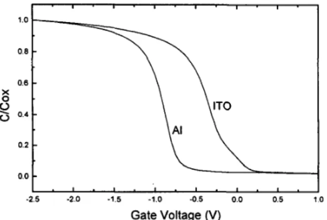
The NMOS diode using transparent electrodes (ITO) has a work function about 0.5 eV lower than AI as measured by C- V (Fig. 11). At the same negative gate bias, the I T 0 gate has a smaller tunneling current with similar IR spectra. The photocurrent of I T 0 detectors increases by a factor of 20 (Fig.
12), as compared to AI devices. The large photocurrent was observed to damage the device by slightly increasing the dark current.
Conclusions
The MOS tunneling diode can serve as both a light emitter and a light detector at a suitable bias. This configuration can be applied in a duplex mode of optical interconnects in ULSI chips as well as the image sensor. The surface band bending is responsible for the bandgap reduction in the sharp emission spectra. High growth temperature of the oxide of the photodetector can reduce the dark current to 3 nA/cm2.
Acknowledgments
This work is supported by National Science Council, Taiwan, R.O.C. under contract numbers: 88-22 18-E-002-004, 88- 22 18-E-002-004, 88-22 15-E-002-02 1 and 88-2 1 12-M-002- 038. The initial support of UMC and TSMC is also highly appreciated.
References
[ l ] K. Misiakos et al., "Monolithic integration of light emitting diodes, detectors, and optical fiber on a silicon wafer: a CMOS compatible optical sensor," IEDM, Tech. Dig. pp.25-28, 1998
[2] Q. Mi et al. "Room-temperature 1.3 pm electro-luminescence from strained SiGelSi quantum wells," Appl. Phys. Lett. 60, pp.3177-3179, 1992. [3] C. W. Liu et al. " Room-temperature electroluminescence from electron-
hole plasmas in the metal oxide silicon tunneling diodes," will submit to Appl. Phys. Lett. 1999.
31.3.2
Gate Voltage (V)
Fig.l. Photo and dark currents of a NMOS tunneling diode. Dark current does not change after light exposure. Device size is 3 ~ 1 0 ~ an2. The photo current was generated by metal halide lamps with spectra similar the sun.
5.0110’0 I
.
,.
I.
,
.
,.
I
--.-measureddataI
at lOOk Hz -0- calibrated data1
-3 -2 1 0 1 2 Gate Voltage (V)Fig. 2. A C-V plot of a NMOS tunneling diode. The thickness measured by ellipsometer is about 2.3nm. The thickness extracted from C-V is 2.6nm. The insert is the equivalent circuit model for extraction.
A1
SiO,
p-Si
Fig. 3. The electron tunneling current and photon emission for NMOS at negative gate bias.
C
’
1 I I h c ‘E-
-4V,6.0Akm2- 3 c -900 1Mx) 1100 1200 x) Energy (meV)Fig. 4. Emission spectra of NMOS tunneling light emitting diodes as well as
theoretical fitting.
-3 1 0 1 2
Gate Voltage 01)
Fig. 5. Photo and dark currents of a PMOS tunneling diode at negative gate bias. Device size is 3x104cm*. Note the large saturation voltage of photo current (- -2V) may be due to large valence band discontinuity ( A E d S e V ) .
Fig. 6. A schematic band diagram to explain the band gap reduction.
31.3.3
I I I I I
900 1000 1100 1200 1300 Energy(meV)
Fig. 7. Emission spectra of PMOS tunneling light emitting diodes as well as
theoretical fitting.
aerec'S
photo current
< < , , A l l ~ = = ~ . 2 e ~ ydark
current
(3Ti"
AEv=4.5eV L - €I 950°C a,-
;
10"9.
1ooo"ch
1tiq3 10"' ".
'.
' * ' * '.
5 Gate Voltage (v)Fig. IO. The dark current of NMOS tunneling light detectors with oxide
grown at different temperature. High growth temperature can decrease the
dark current. The current spike around OV for 1000°C sample may be due to
the tunneling through the interface states.
I " " " " " " '
I T v - I
1 P .
-2.5 -2.0 -1.5 -1.0 -0.5 0.0 0.5
Gate Voltage (V)
Fig. 8. The operation principle for a NMOS tunneling light detector at positive gate bias.
Wavelength (pm) 1.181h
Fig. 9. The detection specbum of a NMOS tunneling detector bias at zero
bias. The tail at 1.1 to 1.18pm may be due to the interface states and surface
band bending.
I
Fig. 11. C-V plots of IT0 gate and AI gate NMOS devices. The work function of IT0 is about 0.5eV lower than AI. This sample is not the same one in Fig. 2. 1E-5
.
,.
,.
,.
,.
,.
,.
,.
1200 mw/cm' after exposure 264 mW/cmzI
-
-150 mW/cm2 before exposure 150 mW/cm2 0 (3 1E-10 dark current before exposure 1E-121
0.0 0.5 1.0 1.5 2.0 2.5 3.0 3.5 4.0 Gate Voltage (V)Fig. 12. Photo and dark currents of a NMOS tunneling diode using a IT0
gate at positive bias. The photo current increases by a factor of 20, compared to the AI gate.