國立交通大學
材料科學與工程研究所
碩士論文
利用閘極掘入方式製作增強型高截止電壓氮化鋁鎵/氮化
鎵/氮化鋁鎵金屬-絕緣體-半導體高電子遷移率電晶體之
研究
Study of Recessed Enhancement-mode AlGaN/GaN/
AlGaN MIS-HEMT with High Threshold Voltage
研究生:
陳奕仲
指導教授
: 張翼 博士
利用閘極掘入方式製作增強型高截止電壓氮化鋁鎵/氮化
鎵/氮化鋁鎵金屬-絕緣體-半導體高電子遷移率電晶體之
研究
Study of Recessed Enhancement-mode
AlGaN/GaN/AlGaN MIS-HEMT with High Threshold
Voltage
研究生 : 陳奕仲 Student: Chen Yi-Chung
指導教授: 張翼博士 Adveisor: Dr. Edward Yi-Chang
國立交通大學
材料科學與工程研究所
碩士論文
A Thesis Submitted to Department of Materials Science and Engineering College of Engineering
National Chiao Tung University In Partial Fulfill of the Requirements
For the Degree of Master of Science
In Material Science and Engineering July 2009
Hsinchu, Taiwan, Republic of China
Contents
Abstract(Chinese) ... VI Abstract(English) ... VIII Acknowledgement ... X Table Captions ... XI Figure Captions ... XII
Chapter 1 Introduction ... 1
Chapter 2 Literature Review ... 4
2-1 The Mechanism of High Electron Mobility Transistor (HEMT) ... 4
2-2 MOS-FET structure ... 6
2-3 Recess techniques ... 7
2-4 Rapid thermal annealing recovery ... 8
2-5 Recessed MIS-HEMT ... 9
Chapter 3 Experiment and Fabrication Process ... 17
3-1 Schottky Diode ... 17
3-1-2 BCl3 Recess ... 18
3-1-3 RTA recovery. ... 18
3-2 Conventional E-mode HEMT structure ... 19
3-2-2 Ohmic Contact Formation ... 19
3-2-3 Mesa Isolation ... 20
3-2-4 Lithography of gate region ... 20
3-2-5 BCl3 Recess ... 20
3-2-6 Gate formation ... 21
3-3 Recessed Enhancement-mode MIS-HEMT Device Fabrication ... 21
3-2-1 Wafer Cleaning ... 21
3-2-2 Ohmic Contact Formation ... 22
3-2-3 Mesa Isolation ... 22
3-2-4 Lithography of 1st gate region ... 22
3-2-5 BCl3 Recess ... 23
3-2-6 RTA recovery ... 23
3-2-7 Si3N4 deposition ... 23
3-2-8 Nitride Via ... 24
3-2-9 Gate formation ... 24
3-4 Depletion mode HEMT fabrication ... 24
Chapter 4 ... 27
Results and Discussion ... 27
4-1-1 Recess etching condition ... 27
4-1-2 Recess Target test for recessed enhancement-mode . ... 28
4-1-3 RTA recess recovery condition test ... 29
4-2 Device performance of conventional E-mode HEMT. ... 30
4-3 Device performance of recessed E-mode MIS-HEMT ... 30
4-4 Device perfromance of D-mode HEMT device. ... 31
Chapter 5 Conclusions ... 39
References……… 40
利用閘極掘入方式製作增強型高截止電壓氮化鋁鎵/氮化
鎵/氮化鋁鎵金屬-絕緣體-半導體高電子遷移率電晶體之
研究
研究生: 陳奕仲 指導教授: 張翼 博士
交通大學材料科學與工程系
摘要
氮化鋁鎵/氮化鎵/氮化鋁鎵增強型高電子遷移率電晶體近幾年來廣 受注目,但由於目前之元件磊晶技術所製作的高電子遷移率電晶體之電流 與電壓接仍偏低,尚無法做商業上之使用。而近年來之研究重點:金-氧-半場效電晶體雖擁有較高的起始電壓,但由於製程上尚未成熟,加上比起 高電子遷移率電晶體其擁有較高的通道電阻,故仍未能通過工業使用標 準。 本研究提出以閘極蝕刻之方式來製作增強型高起始電壓氮化鋁鎵/氮 化鎵/氮化鋁鎵金屬-絕緣體-半導體高電子遷移率電晶體,並建立其標準 化製程。此結構擁有比起金-氧-半場效電晶體較為簡易的製程,並擁有較 低的電阻,同時此結構亦可達到較高之截止電壓。本實驗以蕭特基二極體 做各種製程之參數測試,以找到對元件表現最好的使用條件,並成功建立 金屬-絕緣體-半導體高電子遷移率電晶體之標準製程。此元件擁有2mA/mm 的通道電流,0.8mS/mm 之互導係數,並擁有超過 200V 之崩潰電壓, 更達到了 9V 的高截止電壓。而此結構同時亦可用於製作截止型高電子遷 移率電晶體,擁有 280mA/mm 之電流與 75mS/mm 之電導,同時亦可在高電 壓下操作。
Study of Recessed Enhancement-mode
AlGaN/GaN/AlGaN MIS-HEMT with High Threshold
Voltage
Student: Yi-Chung Chen Advisor: Dr. Edward Yi-Chang
Department of Materials Science and Engineering, National Chiao-Tung University
Abstract
AlGaN/GaN/AlGaN enhancement-mode high electron mobility transistor (HEMT) is extensively studied in recent years. However, there is still no solution to fabricate a HEMT with high threshold voltage, which means that it will cause mis-operation in high voltage operation. For enhancement mode operation (E-mode), metal-oxide-semiconductor field effect transistor (MOS-FET), though it has higher threshold voltage, it is not commercialized due to the immature process techniques and higher on-resistance than HEMT. In this thesis, gate recess technique is used to fabricate E-mode AlGaN/GaN/AlGaN metal-insulator-semiconductor high electron mobility transistor (MIS-HEMT). This structure has simpler process and lower on-resistance in comparison with MOS-FET. Additionally, this structure can achieve very high threshold voltage to avoid the mis-operation of the device.
Schottky diode was used for process parameter evaluation to find out the optimum process condition, and then the recessed E-mode MIS-HEMT standard process was established. The device demonstrated 2 mA/mm, 0.8 mS/mm, and more than 200V for channel current, transconductance, and three-terminal breakdown voltage, respectively. Furthermore, the device shows 9V threshold voltage. The structure can also be applied to conventional D-mode HEMT application with ID = 280mA/mm and Gm = 75
mS/mm. These characteristics indicate that the structure is promising for high voltage electronic applications.
致謝
兩年的日子中,我就在這個實驗室度過了。 從剛來的懵懵懂懂,到現 在的侃侃而談,這之中的轉變不可謂不大。而這些轉變都要歸功於這實驗 室所帶給我的一切。從實驗上的專門知識,為人處事的方法,上台簡報的 技巧,論文寫作的訣竅等,我都學了相當的多。最要感謝的首歸指導教授 張翼老師,從我剛來時就推薦我至台積電實習,讓我先初窺了所謂的製程 技術,後來又在兩年期間對我照顧有加,不吝給予指導,一切令我銘感於 心。再來便是我的指導學長-張家達學長,從我剛來時甚麼都不懂,一步 一步的指點我到可以獨立上台簡報,雖然這之中我重複的問了很多笨問題, 您總是有耐心的給予我指導。而從您身上我也學到了很多為人處事的道理 以及無私的智慧,這些我相信對我未來的生活中有著相當大的幫助,謝謝! 而GaN Group 的阿乾學長、宗育學長、小巴學弟以及前來實習的 David 學弟,感謝您們在實驗和生活中都帶給了我不少色彩,而實驗室的其他人 也給了我相當多的幫助,真的謝謝您們。 除此之外,亦要感謝電子所的鄭兆欽博士,給了我很多專業的建議。更 感謝社團的所有夥伴們,以及許多的朋友,總在我煩悶時給了我許多的歡 笑與依靠。而最重要的,便是我的家人和女友,感謝您們一路支持我,不 離不棄。 今天能成功完成論文,要致謝的人真的太多太多,有您們的祝 福我才能有今天。謝謝!Table Captions
Table.1-1 Property comparison between different materials. ... 3
Table 2-1 E-mode HEMT comparison by different fabrication approach. ... 11
Table 2-2 : MOS-FET performance comparison. ... 12
Table 4-1. Capacitance of the Schottky diode on different recess target. ... 32
Table 4-2. The comparison of leakage current, ideal factor , barrier height at different RTA condition. ... 32
Figure Captions
Fig. 2-1 Energy band-gap of AlGaN/GaN/AlGaN HEMTs. ... 13
Fig 2-2 Device structure of conventional HEMT ... 13
Fig 2-3 Conventional GaN N-MOS structure ... 14
Fig 2-4 The structure of Schottky diode. ... 14
Fig 2-5 Schematic cross section of the proposed AlGaN/GaN/AlGaN recessed MIS- HEMT ... 14
Fig 2-6. Output I–V characteristics of the recessed MIS-HEMT ... 15
Fig 2-7. ID–VG characteristics of the recessed MIS-HEMT at a drain-source voltage of 0.1 V. ... 15
Fig 2-8 Off-state I–V characteristics of the recessed MIS- HEMT measured at a gate bias voltage of 0 V. ... 16
Fig 2-9 Band diagram of the AlGaN/GaN/AlGaN structure ... 16
Fig 3-1. Schematic cross section of the E-mode AlGaN/GaN HEMT device structure. ... 25
Fig 3-2. Schematic cross section of the recessed E-mode AlGaN/ GaN/AlGaN MIS-HEMT device structure. ... 25
Fig 4-1. Leakage current of Schotty diode at different recess time. ... 33
Fig 4-2. Leakage current trend of Schotty diode at different recess time. ... 33
Fig 4-3. C-V curve of the 800s etched Schottky diode. ... 34
Fig 4-4. Leakage current trend on different RTA condtion. ... 34
Fig 4-5. Ideal factor and barrier height trend on different RTA condition ... 35
Fig 4-6. ID-VD curve of the conventional E-mode HEMT device. ... 35
Fig 4-7 ID- VG curve of the conventional E-mode HEMT device. ... 36
Fig 4-8 ID-VD curve of the recessed E-mode MIS-HEMT. ... 36
Fig 4-9. ID-VG curve of recessed E-mode MIS-HEMT. ... 37
Fig. 4-10 Off state breakdown voltage of recessed E-mode MIS-HEMT at Vg= 0V. ... 37
Fig. 4-11. ID-VD curve of D-mode HEMT device. ... 38
Chapter 1
Introduction
In recent years, GaN and the related compounds play more and more important role in power electronics due to its unique properties such as high breakdown voltage ((2×10⁶ V/cm), wide direct band gap (3.4 eV), high saturation velocity (2.2×107cm/s) and large power density compared to other materials as listed in Table 1-1. Due to their superior material properties compared with conventional Si devices, GaN-based electron devices have lately attracted considerable attentions as next-generation devices for power electronic applications such as automobile electronics, satellite, and base station. Among these applications, enhancement-mode (E-mode) devices play a very crucial role. Enhancement mode devices can not only simplify the design of the circuit, but also has lower standby power dissipation and good for fail safety issue.
Several approaches for fabricating E-mode devices have been proposed. For instance, recess techniques [1-2] , which include chlorine based gas to do dry etching beneath the gate region. Other approaches such as p-type gate structure [3–5], thin AlGaN barrier layer [6-8], fluoride-based plasma treatment [9-12], Cat-CVD SiN deposition [13], and p-type gate structure
[14–16], have also been reported. However, the threshold voltage of these devices is not high enough to avoid noise interference for power applications. In hundreds volts operation, a slight noise will cause misoperation of the devices. According to the demand of circuit design for power electronics, a threshold voltage up to 3-5 V is generally required [17].
In order to reach the requirement, metal-oxide-semiconductor field effect transistor (MOS-FET) structure is proposed.[18]-[27]. For GaN-based enhancement -mode MOS-FET, the threshold voltage is generally higher than 3V. However, it has some drawbacks as following: (1) on-resistance is quite lower than high electron mobility transistor (HEMT) since it lacks the two dimension electron gas (2DEG), (2) implant process is required and it means one more processing step than HEMT process is need,(3) there is no mature approach to grow p-type GaN substrate to form n channel. To solve the problems, Sharp Corp. proposed a new structure, recessed MIS-HEMT structure [28]. It owns the advantage of conventional HEMT, which has low on-resistance, and the advantage of MOS-FET, which has high threshold voltage. In this study, standard process of recessed E-mode AlGaN/GaN/AlGaN MIS-HEMT is established and its performance is also characterized.
Table.1-1 Property comparison between different materials.
Property Si GaAs SiC GaN
Energy Gap (eV) 1.11 1.43 3.2 3.4 Critical Breakdown Field (MV/cm) 0.6 0.65 3.5 3.5 Thermal Conductance (W/cm.oK) 1.5 0.5 4.9 1.5 Mobility (cm2/V-s) 1300 6000 600 1500 Power Density (W/mm) ~0.8 ~1.0 2~4 >2 Saturation Velocity (cm/s) 1x10⁷ 1.3x10⁷ 2x10⁷ 2.7x10⁷
Chapter2
Literature Review
2-1 The Mechanism of High Electron Mobility Transistor (HEMT)
Historically, the invention of HEMT is usually attributed to Takashi Mimura (Fujitsu, Japan). However, Ray Dingle and his co-workers in Bell Laboratories also played an important role in the invention of HEMT. It is also called as heterojunction field effect transistor (HFET) or modulation-doped field-effect transistor (MOD-FET). The structure incorporates a junction between two materials with different band gaps (i.e., a heterojunction) as the channel instead of a doped region, as is generally the case for MOS-FETs. It applies two layers to form heterojunction, one is a highly doped wide band gap n-type donor-supply layer (AlGaN in our example) and a non-doped narrow-band gap channel layer with no dopant impurities (GaN in this case). When these two layers are contacted, the original discontinuous band-gap start to bend in order to maintain the same Fermi Level (Ef) and electron affinity.
Therefore, in order to reach the thermal equilibrium, the electrons will flow from wide band-gap AlGaN layer to narrow band-gap GaN layer. The quantum well is formed on the side of GaN layer where the electrons can
move faster.
Since the quantum confinement effect, the two degree electron gas (2DEG) layer is formed. The band-diagram of the HEMT is shown nn Fig. 2-1. This thin layer conducts the electrons with very high concentration, giving the channel very low resistivity. Afterward, the position of the Fermi Level can be modulated by gate voltage (Vg), and the density of the electron in 2DEG is
also changed. That is how AlGaN/GaN HEMT works. Conventional HEMT structure is shown in Fig. 2-2.
There are two working mode of the HEMT devices. One is called the depletion-mode (D-mode), the other is the enhancement-mode (E-mode). The definition of the E-mode device is that there is no current pass between source and drain regions when gate bias equals zero. It also means that the threshold voltage is higher than zero. In HEMT, E-mode is reached when threshold voltage is lower than built-in potential of the material. At this status, the intrinsic depletion region of the gate will block the 2DEG layer and have the device in off states. By applying the positive bias, the depletion region will draw up and hence, the channel is opened. Several E-mode HEMT devices performance are expressed at the Table 2-1.
transconductance (gm). The definition : gm = VI
.
It can be regard as thecapability of the gate to modulate the channel.
2-2 MOS-FET structure
MIS-FET represents for metal-insulator-semiconductor field-effect transistor. When the insulator is oxide layer, it is also can be expressed as MOS (metal-oxide-semiconductor)-FET in particular. The basic principle of the device was first proposed by J.E Lilienfeld in 1925. It is generally used in amplifier or power switch. The device is called NMOS if it has n-channel, on the other hand, it is called PMOS if the channel is p-type. Fig 2-3 shows the conventional structure of GaN NMOS-FET. The MOS-FET is based on the modulation of charge concentration by the capacitance between a body and gate region. The MOS-FET owns two terminals, which have to be highly doped in order to build the channel.. These regions can be either p or n type, but they must be opposite type to the body region. The source and drain are highly doped as signified by a '+' sign after the type of doping. For E-mode NMOS, If VGS> 0, the inversion layer is formed, and a n-channel is formed,
which means the device is turned on.
field effect mobility (µ is required. It expresses the electron mobility in the channel.
Since the
g
m = VID,
for an ideal MOS-FET which worked on the linearregion, according to the formula:
I
D = W µ CL2 V
GSV
TV
DSV
DS]
g
m = W µ CL. V
DSFor the saturation region,
I
D = W µ CLV
GSV
Tgm = W µ CL
. V
GSV
TRecently, GaN MOS-FET is widely studied. Not only the different oxide were applied, such as Sc2O3[18], Ga2O3[19],MgO[20],SiO2 [21-23], HfO2[24],
Al2O3[25-26] , but also the different structure were proposed, such as trench
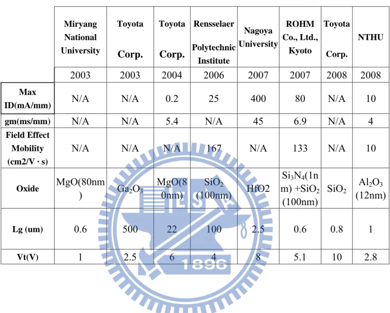
gate structure [27]. A comparison of several MOS-FET performance is shown on Table 2-2.
2-3 Recess techniques
There are two kinds of etching method. For conventional III-V compound semiconductors such as GaAs-based HEMT, it generally uses wet etching method. The main advantage of the wet etching method is it low-damage
characteristic. However, it is hard to find a compatible recipe to etch GaN based devices. Instead, dry etching method is used as the alternative choice. The chloride-based inductive coupled plasma (ICP) reactive ion etching has been employed to etch out the region beneath the gate to increase the transconductance and move the threshold voltage to positive direction since the distance between gate and channel is decreased [29-30], and it has some advantage such as anisotropic etching profile, high aspect ratio etching and it is capable of defining small feature size.
Nevertheless, dry etching will induce damage on the surface since its ion bombardment, which could increase the gate leakage current and decrease the breakdown voltage.
2-4 Rapid thermal annealing recovery
In order to remedy the damage caused by dry etching process, several approaches have been proposed. For example, fluorine-plasma surface treatment method [31] and rapid thermal annealing process [32].
However, the reliability of the fluorine-plasma treatment has not been reported. Therefore, we use RTA method for the experiment in this thesis.
For testing the recess condition and recovery effect, Schottky diode is fabricate to obtain the best performance. Fig 2-4 shows the structure of Schottky diode. The device performance can be well simulated by the condition of Schottky parameters, including the Schottky barrier height ΦB and the ideality factor n. The calculation of the parameters and further performance is expressed as Richardson equation:
I =
I
Sexp
1
I
S= AA
*T
2exp
(-T
)
A
*
= 2qπm
*k
2/h
3where,
IS : Saturation current n : ideal factor A: diode area
A*: effective Richardson constant k: Boltmann’s constant T: absolute temperature
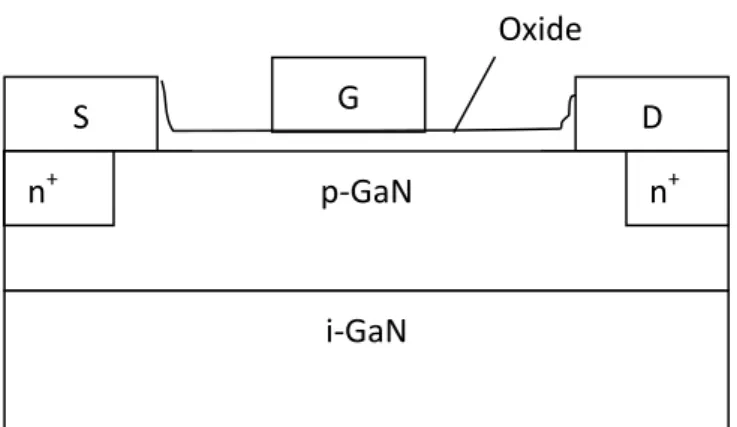
2-5 Recessed MIS-HEMT
The concept of recessed MIS-HEMT is firstly proposed by Sharp Corp [33]. The structure of the device is shown in Fig 2-5. It owns the advantage of high threshold voltage, easier process and lower on-resistance. The epitaxial layer was grown on Si substrate consist of the buffer layer for relaxing the strain. i-GaN layer is the channel layer for 2DEG formation. The AlN above is
for raising the band diagram, and the electrons can be confined better. Al0.25Ga0.75N layer is the barrier layer. And the top GaN layer is the cap layer,
which could suppress the surface state effect.
At the region beneath the gate, cap layer, barrier layer and part of the GaN channel layer are removed. Hence, the 2DEG no longer exist at least on the region under the gate. Therefore, when applied voltage Vgs equal to zero, there is no current can pass from source to drain region. However, when Vgs > 0, the negative polarization charges from the heterojunction below are induced by the positive bias, and form the channel in the region below the gate. Fig 2-6,2-7 and 2-8 shows the device performance.
The mechanism of the device is as the follows: Since the 2DEG region is etched out by recess techniques, current cannot pass when Vg = 0 (Normally-off). When Vg > 0, the polarization-induced negative charges below the gate is attracted and form a channel, the device is turned on accordingly. The band diagram of the structure is shown in Fig. 2-9
Compare to conventional HEMT structure, recessed MIS-HFET owns higher threshold voltage. Furthermore, this structure has lower contact resistance that conventional MOS-FET structure because the 2DEG remains on the region below source and drain region.
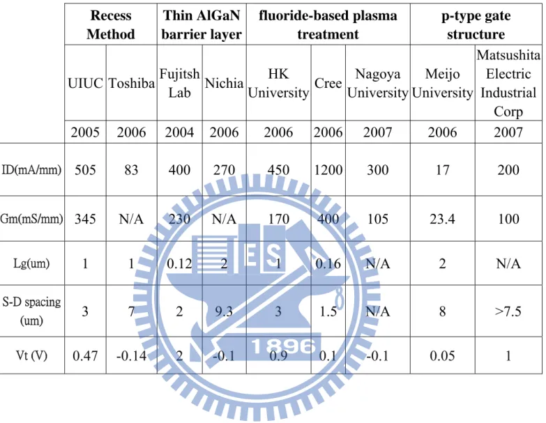
Table 2-1 E-mode HEMT comparison by different fabrication approach. Recess Method Thin AlGaN barrier layer fluoride-based plasma treatment p-type gate structure
UIUC Toshiba Fujitsh
Lab Nichia HK University Cree Nagoya University Meijo University Matsushita Electric Industrial Corp 2005 2006 2004 2006 2006 2006 2007 2006 2007 ID(mA/mm) 505 83 400 270 450 1200 300 17 200 Gm(mS/mm) 345 N/A 230 N/A 170 400 105 23.4 100
Lg(um) 1 1 0.12 2 1 0.16 N/A 2 N/A
S-D spacing
(um) 3 7 2 9.3 3 1.5 N/A 8 >7.5
Table 2-2 : MOS-FET performance comparison.
Miryang National University
Toyota Toyota Rensselaer
Nagoya University ROHM Co., Ltd., Kyoto Toyota NTHU
Corp. Corp. Polytechnic
Institute Corp.
2003 2003 2004 2006 2007 2007 2008 2008
Max
ID(mA/mm) N/A N/A 0.2 25 400 80 N/A 10
gm(ms/mm) N/A N/A 5.4 N/A 45 6.9 N/A 4
Field Effect Mobility (cm2/V · s)
N/A N/A N/A 167 N/A 133 N/A 10
Oxide MgO(80nm ) Ga2O3 MgO(8 0nm) SiO2 (100nm) HfO2 Si3N4(1n m) +SiO2 (100nm) SiO2 (12nm)Al2O3 0.6 500 22 100 2.5 0.6 0.8 1 Lg (um) Vt(V) 1 2.5 6 4 8 5.1 10 2.8
Fig. 2-1 Energy band-gap of AlGaN/GaN/AlGaN HEMTs.
Fig 2-2 Device structure of conventional HEMT
D G
S
Substrate: Sapphire, SiC or Si GaN
Fig 2-3 Conventional GaN N-MOS structure
Fig 2-4 The structure of Schottky diode.
Fig 2-5 Schematic cross section of the proposed AlGaN/GaN/AlGaN recessed MIS-HEMT[28] Oxide G D S n+ n+ p‐GaN i‐GaN Diameter 80μm Schottky Contact Ohmic Contact n+ n+
Fig 2-6. Output I–V characteristics of the recessed MIS-HEMT[28]
Fig 2-7. ID–VG characteristics of the recessed MIS-HEMT
Fig 2-8 Off-state I–V characteristics of the recessed MIS- HEMT measured at a gate bias voltage of 0 V.[28]
Fig 2-9 Band diagram of the AlGaN/GaN/AlGaN structure
Chapter 3
Experiment and Fabrication Process
3-1 Schottky Diode
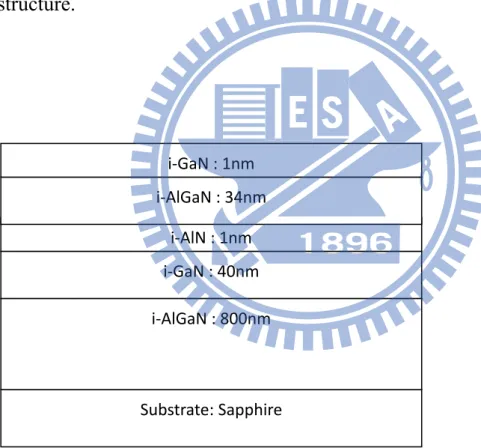
Schottky diode is a good way to indetify the optimized condition of the process. In the experiment, it was tested for recess etching rate, RTA recovery and recess target. The structure of the sample is shown in Fig. 3-1. The AlGaN epitaxial layer was grown on sapphire substrate with buffer layer for relaxing the strain caused by lattice mismatch, an 800 nm thick Al0.05Ga0.95N buffer
layer, a 40-nmthick, GaN channel layer, 34-/1-nm-thick Al0.25Ga0.75N/AlN
barrier layers, and a 1-nm-thick GaN cap layer.
It started from the standard lithography condition and ohmic contact deposition by evaporator afterward. The ohmic contact was composed of Ti(200nm)/Al(120nm)/Ni(25nm)/Au(100nm). Then the wet-solvent lift-off process was carried out to get the ohmic region, followed by a high pressure DI water rinse to remove the residues. After lift-off, the sample was annealed at 800oC for 60 seconds. Then the second lithography was taken to define the gate region.
3-1-2 BCl3 Recess
In order to properly etch out the region below the gate, smooth and stable etching rate was required. In the experiment, ULVAC-NE550 ICP was used to test the etching rate. The etching depth was detected by P-10 analyzer. A slow and steady etch rate was expected to minimize the damage caused by ion-bombardment.
Besides, the optimized recess target was also needed to precisely etch out the 2DEG region. It was followed by gate metal deposition, which was Ni(20nm)/Au(100nm). Several recipes were tested to find the best condition. A C-V curve was tested to find out the best recess target.
3-1-3 RTA recovery.
After recess step, RTA recovery is applied to recover the damage caused by dry etching. We use 400oC as the recovery temperature, and test the performance of samples subjected to different annealing time. RTA-free sample is also fabricated as the comparison. D-C probe and C-V measurement is used to test the devices performance.
3-2 Conventional E-mode HEMT structure
Conventional E-mode HEMT structure was fabricated to confirm the threshold voltage issue and establish standard process. The device structure is shown in Fig. 3-1. The process is as the follows:
3-2-1 Wafer cleaning
The wafer was immersed in ACE and IPA for 5 min, followed by blowing N2 gas. Then the wafer was immersed in BOE:H2O = 1:10 solution for 5
minute and rinsed in D.I water for one minute to etch out the native oxide for the following lithography process.
3-2-2 Ohmic contact formation
An ohmic contact is a low resistance junction formed between a metal and semiconductor. It is formed as the source and drain region electrodes. In order to form a good ohmic contact with low parasitic resistance, Ti(20 nm)/Al(120 nm)/Ni(25 nm)/Au(100 nm) was deposited. After deposition, the wafer was lifted-off in ACE and IPA to remove the unnecessary photoresist. Then the wafer was further immersed in NMD at 80oC for 20 min to clean the residual photoresist. After the lift-off process, the wafer was thermally alloyed at
800oC for 1 min by using RTA to form the ohmic contact.
3-2-3 Mesa isolation
Mesa process was used to isolate each device. We use AZ5214E to define the mesa region. It was carried out by using BCl3 =15 sccm , Cl2 = 25 sccm.
bias RF = 100W , APC = 1.3, PF C= 600 sccm for 150s . Then the wafer was immersed in ACE and IPA followed by D.I water to remove the photoresist. After mesa isolation step, HP4156b Modular DC source/monitor was utilized to measure the ohmic contact resistance and sheet resistance.
3-2-4 Lithography of gate region
Gate region has to be defined for the following recess process. For high frequency and high speed applications, short gate length with low gate resistance is desired. The T-shaped gate structure is the most common approach for obtaining low gate resistance. In order to form a T-gate, Copolymer/PMMA photoresist were used for exposure.
3-2-5 BCl3 recess
After the gate region was defined in the previous step, O2 descum was
the region below the gate. The etching condition was: platen power = 50 W, BCl3 = 10 sccm at 23 mTorr for 350s. After the recess process, the sample was
immersed in ACE and IPA for 10 min to clean the photoresist.
3-2-6 Gate formation
After O2 descum, Ni (20nm)/Au (100nm) was deposited by evaporator to
form the gate region. After deposition, lift-off process was carried out to remove the residual photorresist. D-C probe was used to measure the performance of the conventional E-mode device.
3-3 Recessed Enhancement-mode MIS-HEMT Device Fabrication
The structure is as same as the sample we used in Shcottky diode experiment. Fig 4-2 shows the process flow of the fabrication.
3-2-1 Wafer cleaning
In order to remove the undesirable particles on the surface, the wafer was immersed in ACE and IPA for 5 min, followed by blowing N2 gas. Then the wafer was immersed in BOE:H2O = 1:10 solution for 5 min and rinsed in D.I
water for one minute to etch out the native oxide for the following lithography process.
3-2-2 Ohmic contact formation
As the process in conventional HEMT Structure, Ti (20 nm) /Al (120 nm) /Ni (25 nm)/Au (100 nm) was deposited. After deposition, the wafer is lifted-
off in ACE and IPA to remove the photoresist. Then the wafer is further immersed in NMD at 80oC for 20 min to clean the residual photoresist. After the lift-off process, the wafer is thermally alloyed at 800oC for 1 min by using RTA to form the ohmic contact.
3-2-3 Mesa isolation
AZ5214E is used to define the mesa region. It is carried out by using BCl3
=15 sccm , Cl2 = 25 sccm. RF bias = 100W , APC = 1.3, PFC = 600 sccm for
150s . Then the wafer was immersed in ACE and IPA followed by D.I water to remove the photoresist. After mesa isolation, HP4156b modular DC Source/Monitor is used to measure the ohmic contact resistance and sheet resistance.
3-2-4 Lithography of 1st gate region
Copolymer/PMMA photoresist were used. To overcome the alignment issue, 1μm gate lithography was used here and 3μm gate was used for the 2nd
time gate region.
3-2-5 BCl3 recess
After the gate region was defined in the previous step, O2 descum was
applied for cleaning residual photoresist followed by gate recess to etch out the region below the gate. The conditions are as the follows. The etching condition was: platen power 50 W, BCl3=10 sccm, 23 mTorr for 800s. After
the recess process, the sample was immersed in ACE and IPA for 10minutes to clean the photoresist.
3-2-6 RTA recovery
400oC, 10 min RTA was applied after the gate recess to recover the damage cause by recess. After RTA process, we use P-10 analyzer to confirm the etching depth of the recess region.
3-2-7 Si3N4 deposition
After RTA, the sample was loaded in PECVD to grow Si3N4 as the
insulator layer. The conditions are as follows: Si3H4 is 40 sccm, NH3 =55 sccm
for 2min. n&k analyzer was utilized to evaluate the quality and thickness of Si3N4.
3-2-8 Nitride via
The ohmic contact lithography was applied. Unlike the photoresist in the gate region, AZ5214E was taken for ohmic region formation. After that, the sample was loaded in STS-ICP to etch the oxide layer above the ohmic contact region for the following electrode deposition. Then the sample was rinsed in D.I water for 5min.
3-2-9 Gate formation
The 2nd time gate lithography was utilized. We still use copolymer/ PMMA as the photoresist, and gate length was 3μm for better alignment with the recessed region. After O2 descum, Ni(20 nm)/Au(100 nm) was deposited
by evaporator to form the gate region. After deposition, lift-off process was carried out to remove the residual photorresist.
3-4 Depletion mode HEMT fabrication
The conventional HEMT was also fabricated on the same epitaxial wafer for comparison. The structure of the D-mode HEMT is identical to the recessed MIS- HEMT except for the recessed region and Si3N4 layer. D-mode
Fig 3-1. Schematic cross section of the E-mode AlGaN/GaN HEMT device structure.
Fig 3-2. Schematic cross section of the recessed E-mode AlGaN/GaN/AlGaN MIS-HEMT device structure.
Substrate: Sapphire i‐AlGaN : 800nm i‐GaN : 40nm i‐AlN : 1nm i‐AlGaN : 34nm i‐GaN : 1nm Substrate: Sapphire i‐GaN : 4um i‐AlGaN : 30nm
Fig 3-3 Process flow of the recessed E-mode MIS-HEMT fabrication Ohmic Mesa 1st gate (1um) lithography Recess Recovery Si3N4 Deposition Via Hole 2nd Gate (3um) Measurement
Chapter 4
Results and Discussion
This chapter is divided into four parts. The first part is about the process tuning by Schottky diode, including recess depth, recess target, recovery condition, treatment prior to oxide formation. The second part is about the performance of conventional E-mode HEMT device. Recessed E-mode performance is discussed in the third part. And the last part presents the D-mode HEMT device performance on the same wafer.
4-1 Process condition test by Schottky Diode
4-1-1 Recess etching condition
Schottky diode was fabricated to test the stable etching rate and reliable condition of ICP etching. Since the device performance depends on the etching depth, a slow and stable etching rate is preferred. ULVAC-NE550 was used for this experiment, and the condition is as the following: BCl3 = 20
sccm /platen power = 50 W, Pressure = 3 Pa. By using the P-10 analyzer, it was found that the etching rate is 0.05 nm/s, which is very slow and stable. Additionally, I-V characteristics were also tested to inspect the diode
performance. Fig 4-1 shows the results of Schottky leakage current with etching time. The etching time was increased from 0 to 300s. To clarify the results, Fig. 4-2 plots the leakage current as a function of etching time. The leakage current of the non-etched sample was around 50μA. As etching time was up to 300s, the leakage current was around 3 μA which still remained at the similar current scale with non-etched sample. It could be attributed to the low etching rate which alleviates the surface damage and enhance the reliability of the etching process.
4-1-2 Recess target test for recessed E-mode MIS-HEMT
After the optimum recess etching rate was obtained, the optimized etching depth must be identified. In the experiment, the main purpose of the recess is to etch out the 2DEG channel in the heterojunction layer, therefore, it should have no current at Vg= 0V. Besides, longer time is tested to find out how etching depth correlate to the electron density by C-V test.
After the measurement, we found that at least 700s etching time is required to get the E-mode device. C-V performance as a function of different etching time is shown in Table 5-1. The capacitance of the devices does not show much difference as the etching time increase, which means that all
etching time is applicable as long as it’s longer than 700s. However, from the D-C performance, it is shown that the samples subjected to 1000s and 1200s etching time have high leakage current problem. Based on the leakage current data, 800s etching time was used in this study, which means the 400nm etching depth beneath the gate. Fig. 5-3 shows the C-V curve of the sample with 800s etching. As the voltage increased, the capacitance increased as well since the electrons were accumulated underneath the gate region.
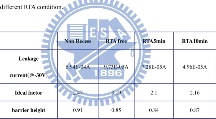
4-1-3 RTA recess recovery condition test
After recess process, the sample was further tested to find out the optimum process condition for damage recovery. Temperature of 400oC was used for 5 min and 10min, and then DC measurement was carried out to identify the trend of leakage current. Furthermore, ideal factor and barrier height were also calculated. Table 4-2 lists the results.
From the comparison between the recessed but RTA-free sample and the sample without recess, it can be found that the leakage current is lower after recess. The result is the same as the results in the leakage current test in section 4-1-1. However, the ideal factor is increased, meaning the forward current performance is worse. After RTA, the 5 min annealed sample posses
ideal factor = 2.1 and the leakage current was 0.728μA. The 10-min annealed sample has ideal factor of 2.16 and leakage current of 0.496μA. The barrier height of all samples are similar. Figs 5-4 and 5-5 shows the trend of the parameters. Therefore, consider both of the leakage current and ideal factor, 10 min RTA was applied in the following experiments.
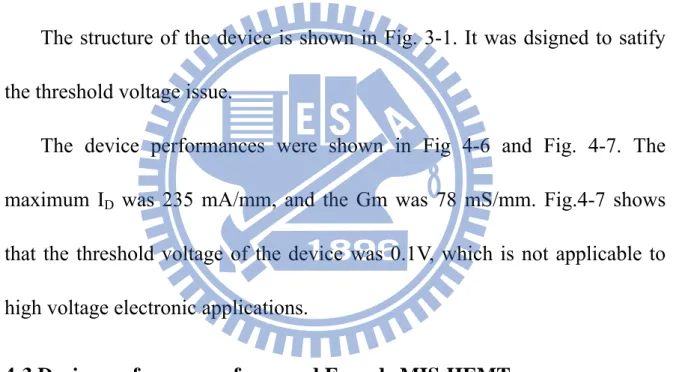
4-2 Device performance of conventional E-mode HEMT.
The structure of the device is shown in Fig. 3-1. It was dsigned to satify the threshold voltage issue.
The device performances were shown in Fig 4-6 and Fig. 4-7. The maximum ID was 235 mA/mm, and the Gm was 78 mS/mm. Fig.4-7 shows
that the threshold voltage of the device was 0.1V, which is not applicable to high voltage electronic applications.
4-3 Device performance of recessed E-mode MIS-HEMT
Figs 4-8,4-9 and 4-10 show the device performances. The maximum ID
was 2 mA/mm, and the transconductance was 0.8 mS/mm. The gm curve didn’t show the highest peak because of the Si3N4 has weak field strength.
Breakdown voltage was larger than 200V, and the threshold voltage was 9V. The result shows that the recessed MIS-gate structure in conjunction with the
polarization-induced negative charges below the gate effectively enhances the threshold voltage of the AlGaN/GaN/AlGaN MIS-HEMT. Compare to Sharp [28], which has ID= 120 mA/mm, the device in the experiment shows lower
forward current. It may due to the different substrate structure. In Sharp’s work, the substrate was Si, however, in this experiment sapphire was used. It is expected that the main current is generated from the heterojunction below, and the different heterojunction condition will cause different electron quantity attracted. The lattice mismatch between the AlGaN with Si and with sapphire is entirely different, hence, the different lattice mismatch will cause the different performance of the devices.
4-4 Device performance of D-mode HEMT device.
The structure is as same as the sample used in recessed E-mode MIS-HEMT. The maximum current achieved was 280 mA/mm, and the gm was 75mS/mm.
Table 4-1. Capacitance of the Schottky diode on different recess target.
Etching time 700s 800s 1000s 1200s
Capacitance(F) 1.6E-12 1.62E-12 1.36E-12 1.5E-12
Table 4-2. The comparison of leakage current, ideal factor , barrier height at different RTA condition.
Non Recess RTA free RTA5min RTA10min
Leakage
current(@-30V)
6.94E-04A 9.73E-05A 7.28E-05A 4.96E-05A
Ideal factor 2.47 3.19 2.1 2.16
Fig 4-1. Leakage current of Schotty diode at different recess time.
Fig 4-2. Leakage current trend of Schotty diode at different recess time.
-30 -25 -20 -15 -10 -5 0 -0.0006 -0.0005 -0.0004 -0.0003 -0.0002 -0.0001 0.0000 0s 40s 60s 80s 120s 150s 250s 300s ID (uA) VD(V) 0 50 100 150 200 250 300 0.0000 0.0001 0.0002 0.0003 0.0004 0.0005 Leakage current(uA) Etching time (s)
Fig 4-3. C-V curve of the 800s etched Schottky diode.
Fig 4-4. Leakage current trend on different RTA condtion.
0 2 4 6 8 10 12 1.10E-012 1.20E-012 1.30E-012 1.40E-012 1.50E-012 1.60E-012 1.70E-012 C(F) V(Volt) 0.00E+00 2.00E‐05 4.00E‐05 6.00E‐05 8.00E‐05 1.00E‐04
RTA free RTA5min RTA10min
Leakage Current(@‐30V)
Fig 4-5. Ideal factor and barrier height trend on different RTA condition
`
Fig 4-6. ID-VD curve of the conventional E-mode HEMT device.
0 0.5 1 1.5 2 2.5 3 3.5
Non Recess RTA free RTA5min RTA10min
Ideal factor barrier height Vg=0V Vg=1V Vg=2V Vg=3V
Fig 4-7 ID- VG curve of the conventional E-mode HEMT device.
Fig 4-8 ID-VD curve of the recessed E-mode MIS-HEMT.
Vt=0.1V Vg=12V Vg=11V Vg=9~10V Vg=13V
Fig 4-9. ID-VG curve of recessed E-mode MIS-HEMT.
Fig. 4-10 Off state breakdown voltage of recessed E-mode MIS-HEMT at Vg= 0V.
Fig. 4-11. ID-VD curve of D-mode HEMT device.
Fig. 4-12. ID-VG curve of D-mode HEMT device.
Vg=‐1V Vg=‐2V
Vg=‐3V Vg=‐4V Vg=0V
Chapter 5
Conclusions
In this study, 0.05 nm/s of recess rate and 400oC RTA for 10 min are the optimized conditions for the recess gate process of enhancement mode device. Conventional E-mode HEMT device was fabricated by recess techniques based on the optimized process conditions are demonstrated. ID= 235 mA/mm
and Gm = 78 mS/mm. Unfortunately, the threshold voltage was 0.1V, which is not suitable for high operational voltage applications. In order to solve the problem, recessed E-mode AlGaN/GaN/AlGaN MIS-HEMT was fabricated. It excibited 2 mA/mm of ID, 0.8 mS/mm of gm, and 9V of threshold voltage. The
process of the E-mode device with high threshold voltage was established. However, the current and transconductance were too low for practical application. D-mode HEMT was also fabricated on the same wafer with the performance of ID = 280mA/mm and gm= 75mS/mm. Further modification on
the device structure is needed to apply the MIS-HEMT technology for E-mode device application.
References
[1]W. B. Lanford, T. Tanaka, Y. Otoki, and I. Adesid, “Recessed-gate enhancement-mode GaN HEMT with high threshold voltage,” Electron. Lett., vol. 41, no. 7, pp. 449–450, Mar. 2005.
[2] W. Saito, Y. Takada, M. Kuraguchi, K. Tsuda, and I. Omura, “Recessedgate structure approach toward normally off high-voltage AlGaN/GaN HEMT for power electronics applications,” IEEE Trans. Electron Devices, vol. 53, no. 2, pp. 356–362, Feb. 2006.
[3] X. Hu, G. Simin, J. Yang, M. Asif Khan, R. Gaska, and M. S. Shur, “Enhancement mode AlGaN/GaN HFET with selectively grown pn junction gate,” Electron. Lett., vol. 36, no. 8, pp. 753–754, Apr. 2000.
[4] N. Tsuyukuchi, K. Nagamatsu, Y. Hirose, M. Iwaya, S. Kamiyama, H. Amano, and I. Akasaki, “Low-leakage-current enhancement-mode AlGaN/GaN heterostructure field-effect transistor using p-type gate contact,” Jpn. J. Appl. Phys., vol. 45, no. 11, pp. L319–L321, Mar. 2006. [5] Y. Uemoto, M. Hikita, H. Ueno, H. Matsuo, H. Ishida, M. Yanagihara, T. Ueda, T. Tanaka, and D. Ueda, “Gate injection transistor (GIT)—A normally-off AlGaN/GaN power transistor using conductivity modulation,”
IEEE Trans. Electron Devices, vol. 54, no. 12, pp. 3393–3399, Dec. 2007.
[6] N. Ikeda, J. Li, and S. Yoshida, “Normally-off operation power AlGaN/GaN HFET,” in Proc. Int. Symp. Power Semicond. Devices ICs, 2004, pp. 369–372.
[7] A. Endoh, Y. Yamashita, K. Ikeda, M. Higashiwaki, K. Hikosaka, T. Matsui, S. Hiyamizu, and T. Mimura, “Non-recessed-gate
enhancement-mode AlGaN/GaN high electron mobility transistors with high RF performance,” Jpn. J. Appl. Phys., vol. 43, no. 4B, pp. 2255–2258, Apr. 2004.
[8]Y. Ohmaki, M. Tanimoto, S. Akamatsu, and T. Mukai, “Enhancementmode AlGaN/AlN/GaN high electron mobility transistor with low on state resistance and high breakdown voltage,” Jpn. J. Appl. Phys., vol. 45, no. 44, pp. L1168–L1170, Nov. 2006.
[9] Y. Cai, Y. Zhou, K. M. Lau, and K. J. Chen, “Control of threshold voltage of AlGaN/GaN HEMTs by fluoride-based plasma treatment: From depletion mode to enhancement mode,” IEEE Trans. Electron Devices, vol. 53,
no. 9, pp. 2207–2215, Sep. 2006.
Chen, “Integration of enhancement and depletion-mode AlGaN/GaN MIS-HFETs by fluoride-based plasma treatment.” Phys. sat. sol. (a) 204, No 6, 2023-2027 (2007)
[11]T. Palacios, Student Member, IEEE, C.-S. Suh, A. Chakraborty, S. Keller, S. P. DenBaars, Senior Member, IEEE, and U. K. Mishra, Fellow, IEEE "High-Performance E-mode AlGaN/GaN HEMTs" IEEE ELECTRON DEVICE LETTERS, VOL. 27, NO. 6, JUNE 2006
[12]H. Mizuno, S. Kishimoto, K. Maezawa, and T. Mizutani, “Quasinormally- off AlGaN/GaN HEMTs fabricated by fluoride-based plasma
treatment,” Phys. Stat. Sol. (C), vol. 4, no. 7, pp. 2732–2735, Jul. 2007.
[13] Masataka Higashiwaki, Takashi Mimura, Fellow, IEEE, and Toshiaki Matsui, Member, IEEE, “Enhancement- Mode AlN/GaN HFETs Using Cat-CVD SiN”, IEEE TRANSANCTIONS ON ELECTRON DEVICES, VOL.54, NO6,JUNE07.
[14] X. Hu, G. Simin, J. Yang, M. Asif Khan, R. Gaska, and M. S. Shur, “Enhancement mode AlGaN/GaN HFET with selectively grown pn junction gate,” Electron. Lett., vol. 36, no. 8, pp. 753–754, Apr. 2000.
[15] N. Tsuyukuchi, K. Nagamatsu, Y. Hirose, M. Iwaya, S. Kamiyama, H. Amano, and I. Akasaki, “Low-leakage-current enhancement-mode
AlGaN/GaN heterostructure field-effect transistor using p-type gate contact,” Jpn. J. Appl. Phys., vol. 45, no. 11, pp. L319–L321, Mar. 2006. [16] Y. Uemoto, M. Hikita, H. Ueno, H. Matsuo, H. Ishida, M. Yanagihara, T. Ueda, T. Tanaka, and D. Ueda, “Gate injection transistor (GIT)—A normally-off AlGaN/GaN power transistor using conductivity modulation,” IEEE Trans. Electron Devices, vol. 54, no. 12, pp. 3393–3399, Dec. 2007 [17]T. Kachi, “GaN power devices for automotive applications,” in Proc. IEEE Compound Semicond. IC Symp. Tech. Dig., 2007, pp. 13–16.
[18]R. Mehandru, B. Luo, J. Kim, and F. Ren"AlGaNÕGaN metal–oxide– semiconductor high electron mobility transistors using Sc2O3 as the gate oxide and surface passivation" APPLIED PHYSICS LETTERS VOLUME 82, NUMBER 15 14 APRIL 2003
[19] Yoshitaka Nakanoa and Tetsu Kachi," Electrical properties of thermally oxidized p-GaN metal–oxide–semiconductor diodes" APPLIED PHYSICS LETTERS VOLUME 82, NUMBER 15 14 APRIL 2003
[20] Y. Irokawa, Y. Nakano, M. Ishiko, and T. Kachi, "MgOÕp-GaN enhancement mode metal-oxide semiconductor field-effect transistors" APPLIED PHYSICS LETTERS VOLUME 84, NUMBER 15 12 APRIL 2004.
[21]Heon-Bok Lee, Hyun-Ick Cho, Kyong-Hum Back, Hyun-Su An, Jung-Hee Lee and Sung-Ho Hahm "Normally-Off GaN n-MOSFET with Schottky-Barrier Source and Drain on a p-GaN on Silicon Substrate." IEEE 2005
[22]Heon-Bok Lee, Hyun-Ick Cho, Hyun-Su An, Young-Ho Bae, Myoung-Bok Lee, Jung-Hee Lee, and Sung-Ho Hahm " A Normally Off GaN n-MOSFET With Schottky-Barrier Source and Drain on a Si-Auto-Doped p-GaN/Si" IEEE ELECTRON DEVICE LETTERS, VOL. 27, NO. 2, FEBRUARY 2006
[23]W. Huang, T. Khan, and T. P. Chow "Enhancement-Mode n-Channel GaN MOSFETs on p and n-GaN/Sapphire Substrates" IEEE ELECTRON DEVICE LETTERS, VOL. 27, NO. 10, OCTOBER 2006
[24] S. Sugiura, S. Kishimoto, T. Mizutani, M. Kuroda, T. Ueda
and T. Tanaka"Enhancement-mode n-channel GaN MOSFETs fabricated on p-GaN using HfO2 as gate oxide" ELECTRONICS LETTERS 16th August 2007 Vol. 43 No. 17
[25] Y.Q. Wu a, P.D. Ye , G.D. Wilk , B. Yang "GaN metal-oxide-semiconductor field-effect-transistor with atomic layer deposited Al2O3 as gate dielectric "Materials Science and Engineering B 135 (2006)
282–284
[26] Y. C. Chang, W. H. Chang, H. C. Chiu, L. T. Tung, C. H. Lee, K. H. Shiu, M. Hong,1,a J. Kwo,J. M. Hong, and C. C. Tsai "Inversion-channel GaN metal-oxide-semiconductor field-effect transistor with atomic-layer-deposited Al2O3 as gate dielectric" APPLIED PHYSICS LETTERS 93, 053504 (2008) [27] Hirotaka OTAKE, Shin EGAMI, Hiroaki OHTA, Yasushi NANISHI1, and Hidemi TAKASU"GaN-Based Trench Gate Metal Oxide Semiconductor Field Effect Transistors with Over 100 cm2/(V s) Channel Mobility"Japanese Journal of Applied Physics Vol. 46, No. 25, 2007, pp. L599–L601
[28] Tohru Oka, Senior Member, IEEE, and Tomohiro Nozawa"AlGaN/GaN Recessed MIS-Gate HFET With High-Threshold-Voltage Normally-Off Operation for Power Electronics Applications" IEEE ELECTRON DEVICE LETTERS, VOL. 29, NO. 7, JULY 2008
[29] Wen-Kai Wang, Po-Chen Lin, Ching-Huao Lin, Cheng-Kuo Lin, Yi-Jen Chan, Senior Member, IEEE, Guan-Ting Chen, and Jen-Inn Chyi, Senior Member, IEEE” Performance Enhancement by Using the n+-GaN Cap Layer and Gate Recess Technology on the AlGaN–GaN HEMT Fabrication” IEEE ELECTRON DEVICE LETTERS, VOL. 26, NO. 1, JANUARY 2005
SELVARAJ and Hiroyasu ISHIKAWA "On the Effects of Gate-Recess Etching in Current-Collapse of Different Cap Layers Grown AlGaN/GaN High-Electron-Mobility Transistors" Japanese Journal of Applied Physics Vol. 45, No. 8, 2006, pp. L220–L223
[31] L. Shen, ―Unpassivated High Power Deeply Recessed GaN HEMTs With Fluorine-Plasma Surface Treatment∥ IEEE Vol. 27, (2006) 214-216. [32] V. Kumar, ―Recessed 0.25um gate AlGaN/GaN HEMTs on SiC with high gate-drain breakdown voltage using ICP-RIE.∥ Electronics Letters Vol.37, (2001) 1483-1485.
[33] Tohru Oka, Senior Member, IEEE, and Tomohiro ozawa"AlGaN/GaN Recessed MIS-Gate HFET With High-Threshold-Voltage Normally-Off Operation for Power Electronics Applications"IEEE ELECTRON DEVICE LETTERS, VOL. 29, NO. 7, JULY 2008

![Fig 2-7. I D –V G characteristics of the recessed MIS-HEMT at a drain–source voltage of 0.1 V.[28]](https://thumb-ap.123doks.com/thumbv2/9libinfo/8255116.171855/28.892.135.701.135.971/fig-characteristics-recessed-mis-hemt-drain-source-voltage.webp)
![Fig 2-8 Off-state I–V characteristics of the recessed MIS- HEMT measured at a gate bias voltage of 0 V.[28]](https://thumb-ap.123doks.com/thumbv2/9libinfo/8255116.171855/29.892.152.628.130.436/fig-state-characteristics-recessed-mis-hemt-measured-voltage.webp)