Low-frequency noise in n-channel metal-oxide-semiconductor field-effect transistors
undergoing soft breakdown
Ming-Jer Chen, Ting-Kuo Kang, Yuan-Hwa Lee, Chuan-Hsi Liu, Yih J. Chang, and Kuan-Yu Fu
Citation: Journal of Applied Physics 89, 648 (2001); doi: 10.1063/1.1333029 View online: http://dx.doi.org/10.1063/1.1333029
View Table of Contents: http://scitation.aip.org/content/aip/journal/jap/89/1?ver=pdfcov Published by the AIP Publishing
Articles you may be interested in
Low-frequency noise characteristics of HfSiON gate-dielectric metal-oxide-semiconductor-field-effect transistors Appl. Phys. Lett. 86, 082102 (2005); 10.1063/1.1866507
Effect of magnetic field on random telegraph noise in the source current of p-channel metal–oxide–semiconductor field-effect transistors
Appl. Phys. Lett. 83, 710 (2003); 10.1063/1.1596381
Low-frequency noise overshoot in ultrathin gate oxide silicon-on-insulator metal–oxide–semiconductor field-effect transistors
Appl. Phys. Lett. 82, 1790 (2003); 10.1063/1.1561575
Origin of microwave noise from an n-channel metal–oxide–semiconductor field effect transistor J. Appl. Phys. 92, 6679 (2002); 10.1063/1.1518763
Random telegraph signals and low-frequency noise in n-metal–oxide–semiconductor field-effect transistors with ultranarrow channels
Appl. Phys. Lett. 76, 3259 (2000); 10.1063/1.126600
Low-frequency noise in
n
-channel metal-oxide-semiconductor field-effect
transistors undergoing soft breakdown
Ming-Jer Chen,a) Ting-Kuo Kang, and Yuan-Hwa Lee
Department of Electronics Engineering, National Chiao-Tung University, Hsin-Chu, Taiwan, Republic of China
Chuan-Hsi Liu, Yih J. Chang, and Kuan-Yu Fu
United Microelectronics Corporation, Science-Based Industrial Park, Hsin-Chu, Taiwan, Republic of China 共Received 11 July 2000; accepted for publication 22 October 2000兲
For 3.3-nm thick gate oxide n-channel metal-oxide-semiconductor field-effect transistors subject to a stress gate voltage of 5.5 V, three distinct events are encountered in the time evolution of the gate current: stress-induced leakage current共SILC兲, soft breakdown 共SBD兲, and hard breakdown 共HBD兲. The localization of SBD and HBD paths, as well as their developments with the time, is determined electrically, showing random distribution in nature. At several stress times, we interrupt the stressing to measure the drain current low-frequency noise power Sid. As expected, Sid follows up the spontaneous changes at the onset of SBD and HBD. The Sid spectra measured in fresh and SILC mode are reproduced by a literature model accounting for the carrier number and surface mobility fluctuations in the channel, and, as a result, both preexisting and newly generated trap densities are assessed. The post-SBD Siddoes originate from current fluctuations in the SBD percolation paths, which can couple indirectly to drain via underlying channel in series, or directly to drain if the SBD path is formed close to drain extension. In particular, a fluctuation in Sid itself in the whole SBD duration is observed. This phenomenon is very striking since it indeed evidences the dynamic percolation origin concerning the trapping–detrapping processes in and around the SBD paths. The subsequent HBD duration remarkably features a flat Sid, indicating the set-up of a complete conductive path prevailing over the trapping–detrapping processes. © 2001 American Institute of Physics. 关DOI: 10.1063/1.1333029兴
I. INTRODUCTION
Soft breakdown 共SBD兲, also called B-mode stress-induced leakage current 共SILC兲 共Ref. 1兲 and quasibreakdown,2 is currently a highly challenging issue in metal-oxide-semiconductor field-effect transistors
共MOSFETs兲 having ultrathin 共⬍5 nm兲 gate oxides.1–7
Cur-rent or voltage fluctuations, as described earlier in Refs. 8 and 9, are a primary highlight of the SBD phenomena re-ported so far.4,5,10,11 The trapping–detrapping processes in and around certain SBD percolation paths as the origin of the fluctuation mode are well recognized.4,5,8–11In particular, the dynamic percolation model12 advances in-depth understandings.13 Among many conventional schemes, the low-frequency noise of gate current exhibits the ability of very sensitively detecting the spontaneous changes due to SBD.5 On the other hand, the drain current low-frequency noise power Sid, a measure of the fluctuation of the drain current in the frequency domain, traditionally serves as monitor of the hot carrier robustness and probe of the oxide traps.14–17The associated mechanism is well defined in terms of the carrier number and surface mobility fluctuations and a unified, analytic model is built up.17However, no extension to the case of soft breakdown is carried out yet. A coupling theory5is recently proposed by relating post-SBD Sidto cur-rent fluctuations in the SBD percolation paths; however,
ex-perimental evidence is lacking and the effect of the SBD-path location is not fully clarified. Very recently, the fundamental differences and similarities between SBD and HBD attract much attention;18–21 however, no comparisons on low-frequency noise are performed.
The aim of this study is to explore the merits of Sid characterization while undergoing soft breakdown, with which current understandings concerning the origins of SILC, SBD, and HBD can all be substantially improved. First of all, the localized SBD and HBD paths each are de-termined electrically. This is essential prior to analyzing Sid data. Second, the measured Sid indeed follows up the spon-taneous changes at the onset of SBD and HBD. Third, both preexisting and newly generated trap densities are extracted using pre-SBD Siddata. Fourth, the amount of post-SBD Sid depends strongly upon the location of the SBD path, con-firming the mentioned coupling theory. Fifth, in the whole SBD duration a fluctuation in Sid is observed for the first time. This striking phenomenon evidences the so-called dy-namic percolation origin. Eventually, a quite flat Sid is no-ticed in the whole HBD duration, significantly different from SBD.
II. EXPERIMENTS
The n-channel MOSFETs under study were fabricated in a 0.18m process. In this process, the gate oxide was ther-mally grown in a dilute oxygen ambient, and the polysilicon
a兲Electronic mail: [email protected]
JOURNAL OF APPLIED PHYSICS VOLUME 89, NUMBER 1 1 JANUARY 2001
648
0021-8979/2001/89(1)/648/6/$18.00 © 2001 American Institute of Physics
gate was arsenic implanted at 50 keV and 2⫻1015cm⫺2, followed by N2 and O2annealing. The gate oxide size drawn
was 10⫻10 m2, and the physical oxide thickness was 3.3 nm as determined by a C – V method accounting for polysili-con depletion and quantum mechanical effects. A polysili-constant gate voltage of 5.5 V was adopted to stress gate oxide, with source, drain, and substrate tied to ground. The high-field stressing was interrupted several times for characterization of the threshold voltage Vth, the transconductance gm, and the low-frequency noise power spectrum of drain current. The bias conditions used were共i兲 VD⫽0.1 V for drain current vs gate voltage characteristics, from which Vth and gm were extracted above threshold; and 共ii兲 VD⫽0.1 V and VG⫽1 V for Sidin channel inversion. Figure 1 illustrates the measure-ment set-up, comprising a HP 35665A dynamic signal ana-lyzer, BTA 9603 FET noise anaana-lyzer, and HP 4156B semi-conductor parameter analyzer. The measurement frequency ranged from 1 Hz to 1 kHz. Three noise filters were used to eliminate the residual noise in all bias sources. In our work the Sid data were the average of the total 20 measurements for each frequency. It was found that Siddiffers significantly sample by sample.
III. DETAILED RESULTS A. Sample #1
The evolution of the gate current IG during constant voltage stressing is depicted in Fig. 2, showing the sponta-neous changes as denoted by three critical time points: the time to first SBD TSBD1共⬇20 s), the time to secondary SBD TSBD2共⬇100 s), and the time to HBD THBD共⬇230 s). The gate current following each of the SBD events exhibits fluc-tuations as partially magnified in Fig. 3 for TSBD1⬍t
⬍TSBD2, while relatively few fluctuations were found not
only in the SILC duration共i.e., 0⬍t⬍TSBD1) but also in the
HBD duration (t⬎THBD). The current fluctuations in Fig. 3
arise from the trapping–detrapping processes in and around the SBD paths. An analysis of such fluctuations by following the treatments13led to the behavior of a non-Gaussian
statis-tical distribution. Also plotted in Fig. 2 are the other terminal currents simultaneously measured, with which the percola-tion paths can be identified. First of all, the drain current ID is comparable to the source current ISin the first SBD dura-tion, indicating that the first-SBD percolation path is located around midchannel, far from source/drain. As to the second-ary SBD, a sudden increase is noticed in IS while ID is al-most unchanged. This suggests that the secondary SBD path appear over the source corner. Eventually, a HBD path is formed close to drain extension as reflected by sudden in-crease in ID and unchanged IS in Fig. 2 for t⬎THBD. The corresponding percolation paths are schematically plotted in Fig. 4, where the spheres represent the traps generated during the stress. These paths are drawn based on the recent research21on the same oxide thickness; the critical trap num-ber per cell nBDis three for SBD path, while in HBD path
nBD is four. In the HBD percolation, the traps spans the
FIG. 1. Schematic diagram of the drain current noise measurement system. FIG. 2. Measured terminal currents versus stress time under constant volt-age stressing for sample #1. The constant voltvolt-age of VG⫽5.5 V is for
Fowler–Nordheim共F–N兲 tunneling stress. There may be a third SBD event quickly following TSBD2due to sudden current change.
FIG. 3. Detailed evolution of the gate current corresponding to Fig. 2 after the occurrence of the first SBD.
649
J. Appl. Phys., Vol. 89, No. 1, 1 January 2001 Chenet al.
whole oxide to connect one plate to the other one, while for the SBD path such plate-to-plate connection is incomplete as characterized by the remaining oxide thickness over the lo-calized physically damaged region 共like the shaded spheres in Fig. 4兲 according to the theory.2
The above time to breakdown parameters were defined in terms of sudden increase in gate current. This definition is adequate since it was found that after TSBD1 or TSBD2 the
poststress gate current vs gate voltage characteristic curves resembled the direct tunneling one of the fresh oxide with thinner thickness, whereas it became Ohmic after THBD.
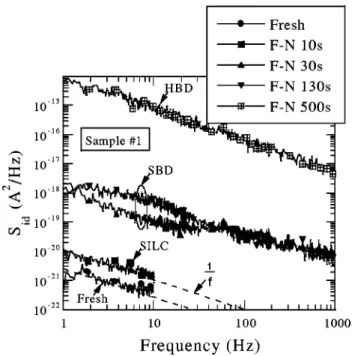
Fig-ure 5 shows the drain current IDvs gate voltage characteris-tics monitored at VD⫽0.1 V for several stress times. These curves seem to shift toward the positive gate voltage direc-tion with increasing stress time until the catastrophic hard breakdown occurs. This proves the fact that part of the tun-neling electrons are trapped in the oxide and the trap number increases with the time. It was found that regardless of SBD, both Vthand gmdegradations showed weak dependencies, in agreement with the citation.5 Figure 6 shows the measured drain current noise power spectrum for different stress times. A view of this figure reveals that Sid in the SILC mode increases, then experiencing orders of magnitude increase at the onset of the SBD, again followed by another order of magnitude increase at the onset of the HBD. The post-Sid data in some frequency range may be able to fit the 1/f␥ relationship with the power exponent ␥ very close to unity; however, significant deviations occur for the remaining fre-quency range. This indicates the existence of the typical Lorentzian spectrum as validated by the aforementioned non-Gaussian distributions deduced from current fluctuations in Fig. 3.
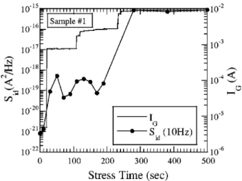
Figure 7 shows the normalization of noise power (⫽Sid/ID
2) vs the gate current I
Gat the same bias condition as the noise measurement. This figure is highly valuable since it exhibits a significant correlation with which Sid can be ad-equately traced to gate current. On the other hand, the Sidfor a certain measurement frequency can readily follow up the spontaneous changes in gate current during the stressing, as together plotted in Fig. 8. Particularly, two phenomena of concern can be drawn herein. One is the Sidfluctuation in the whole SBD duration, looking like a damped sinusoidal waveform. This is the case with high confidence since we have repeated measurements considerably to ensure a smooth and stationary noise spectra. The other is a quite flat Sid in the subsequent HBD duration, significantly different FIG. 4. Schematic cross-section view of the first sample, which shows the
SILC mode, the localized SBD paths, and the HBD path, all corresponding to Fig. 2.
FIG. 5. Measured drain current ID vs gate voltage VG curves with VD
⫽0.1 V for several stress times.
FIG. 6. Measured drain current noise spectra (Sid) with VD⫽0.1 V and
VG⫽1 V for several stress times.
650 J. Appl. Phys., Vol. 89, No. 1, 1 January 2001 Chenet al.
from SBD. This is consistent with the set-up of a complete conductive path prevailing over the trapping–detrapping pro-cesses.
B. Sample #2
Figure 9 shows the evolution of the gate current under the same stress condition for another sample labeled #2, showing the SBD events followed by HBD. The SBD and HBD paths are located accordingly and the results are de-picted in Fig. 10. It is argued that the first SBD and the final HBD paths are formed near drain due to sudden rise in drain current, whereas the second SBD path is formed close to source due to sudden rise in source current. Figure 11 shows the measured Sidfor the first SBD and final HBD along with those from the first sample. It can be seen that the first SBD event of the second sample produces Sidabout two orders of magnitude larger than the first sample.
IV. ORIGINS OFSid
A. Carrier number and surface mobility fluctuations
The power exponent␥of⬇1 for pre-SBD noise data in Fig. 6 indicates that the traps are spatially uniformly distrib-uted within the oxide. The density of the traps responsible, NTin cm⫺3eV⫺1, comprises the pre-existing one N0and the
newly generated one. Since the latter empirically obeys a power law dependency on the stress time,22–24we get explic-itly
NT⫽N0⫹K⫻t0.5, 共1兲
FIG. 7. A correlation plot between normalized drain current noise at 10 Hz frequency and gate current, all from the same bias condition of VD⫽0.1 V
and VG⫽1 V.
FIG. 8. Measured stress time dependencies of drain current noise at 10 Hz frequency and gate current for comparison. Here the gate current was moni-tored at VG⫽5.5 V during the stressing.
FIG. 9. Measured terminal currents vs stress time under constant voltage stressing for another sample #2.
FIG. 10. Cross-section diagrams showing the SILC mode and the localized SBD and HBD paths for another sample #2.
651
J. Appl. Phys., Vol. 89, No. 1, 1 January 2001 Chenet al.
where K is a constant to be fitted. Under the same situation
共i.e., uniform distribution for the traps兲, a unified, analytic
model17dealing with the carrier number and surface mobility fluctuations can be exactly cited,
Sid⫽ kTID2 ␥0f WL
冉
1 N⫹␣兲
2⫻N T, 共2兲where q is the electron charge; N is the number of channel carriers per unit area;␣is the scattering coefficient;is the carrier mobility; ␥0(⫽1.29⫻108cm⫺1) 共Ref. 17兲 is the
at-tenuation coefficient of the electron wave function in the oxide; and W and L are the channel width and length, respec-tively. We now demonstrate how to extract N0 and K from
fresh and SILC noise data. First of all, the device parameters at t⫽0 as drawn from fresh I – V at VD⫽0.1 V in Fig. 5 are ID⫽2.0⫻10⫺5A, gm⫽3.0⫻10⫺5S, and Vth⫽0.32 V.and
N can be straightforward calculated using the formula, ⫽gmL/(Cox⫻VD⫻W) and N⫽(Cox/q)(VG⫺Vth⫺VD), where Coxis the gate capacitance per unit area. As a result, a
fitting to fresh Sid data in Fig. 6 produces N0⫽5.0
⫻1016cm⫺3eV⫺1 for ␣⫽2.0⫻10⫺15V s. The extracted N 0
respective to used ␣is reasonable as compared with the re-ported dependencies.17In a similar way, constant K was ex-tracted to be 6.6⫻1016cm⫺3eV⫺1s⫺0.5based on Sid data at t⫽10 s.
With known K and N0, the drain current noise solely
due to the carrier number and surface mobility fluctuations can readily be assessed using Eqs.共1兲 and 共2兲. The amount of the traps increases with the stress until a critical number triggering soft breakdown is encountered. The corresponding traps constitute a percolation path. We assume that outside of the percolation paths, the traps still continue increasing in number with time after SDB events according to Eq. 共1兲. This is valid in nature since essentially the time to soft break-down parameters such as TSBD1 and TSBD2 are statistically
independent of each other.18–21The calculated drain current noise 共the input parameters like ID, Vth, and gm were all from Fig. 5兲 was found to be negligible respective to SBD
data in Fig. 6. This figures out the origin of post-SBD Sidfar away from the conventional carrier number and surface mo-bility fluctuations.
B. Current fluctuations in SBD percolation paths
In view of several supporting evidences, we favor gate current fluctuations 共see Fig. 3兲 in the localized SBD perco-lation paths as the origin of the post-SBD drain current noise; that is, current fluctuations can couple from certain SBD paths through the underlying channel in series, thus bringing noise to the drain. The first evidence is a fluctuation mode in Sidin Fig. 8. This phenomenon is possible to eluci-date only based on the dynamic percolation model12,13or the dynamic trapping–detrapping processes in and around the SBD percolation paths. Also found in Fig. 8 is the second evidence in terms of a flat Sidin HBD duration, which can in turn strengthen the first evidence. This is because if the Sid fluctuation were not absent in HBD duration, the dynamic percolation origin would not be suitable in SBD duration.
The first SBD Siddiffers significantly sample by sample as revealed in Fig. 11. This can essentially be traced to the different locations of that SBD path, or equivalently to the presence and absence of the underlying channel in series, respectively. This new finding serves as the third evidence. Two plausible interpretations are presented here. First, in sample #1 the first SBD path is farther from drain and, as a result, the underlying channel in series is resistant to the coupling action, effectively lowering the coupling efficiency. The so-called coupling action is that the trapping and detrap-ping processes can modulate directly or indirectly the under-lying channel potential according to the equivalent circuit published elsewhere.5The correlation plot in Fig. 7 can serve as a supporting evidence of this theory. Second, the series channel is bypassed in sample #2 since the first SBD path formed is close to the drain extension, making possible the coupling to affect in a direct manner. No such dramatic dif-ferences are found in HBD duration, as expected since the percolation paths responsible are all formed close to the drain.
V. SUMMARY
The localized SBD and HBD paths have been located electrically for n-channel MOSFETs undergoing soft break-down. This enables efficient analyses of Siddata. As a result, current understandings concerning the origins of SILC, SBD, and HBD have all been substantially improved. What we have achieved saliently are共i兲 the Sid indeed follows up the spontaneous changes at the onset of SBD and HBD;共ii兲 the Sid data in fresh and SILC mode contain information about the preexisting and newly generated trap densities; 共iii兲 the effect of the SBD-path location is significantly clarified, thus confirming the coupling theory; 共iv兲 a Sid fluctuation in the whole SBD duration evidences the dynamic percolation ori-gin; and 共v兲 eventually a quite flat Sid in the whole HBD duration points out a complete conductive path dominating. FIG. 11. Comparisons of the measured Sidunder the bias condition of VD
⫽0.1 V and VG⫽1 V in the first SBD and the final HBD for two samples.
652 J. Appl. Phys., Vol. 89, No. 1, 1 January 2001 Chenet al.
ACKNOWLEDGMENTS
The authors would like to thank M. J. Chang for per-forming C – V fitting, and Dr. H. T. Huang and K. N. Yang, Reliability Physics Laboratory, for their stimulating discus-sions. This work was supported by the National Science Council under Contract No. 89-2215-009-049.
1
K. Okada, S. Kawasaki, and Y. Hirofuji, Extended Abstracts of 1994 International Conference on Solid State Devices and Materials共SSDM兲, 1994, p. 565.
2S. H. Lee, B. J. Cho, J. C. Kim, and S. H. Choi, International Electron
Devices Meeting共IEDM兲, Tech. Dig., 1994, p. 605.
3
T. Yoshida, S. Miyazaki, and M. Hirose, Extended Abstracts of 1996 International Conference on Solid State Devices and Materials共SSDM兲, 1996, p. 539.
4M. Depas, T. Nigam, and M. M. Heyns, IEEE Trans. Electron Devices 43,
1499共1996兲.
5B. E. Weir, P. J. Silverman, D. Monroe, K. S. Krisch, M. A. Alam, G. B.
Alers, T. W. Sorsch, G. L. Timp, F. Baumann, C. T. Liu, Y. Ma, and D. Hwang, International Electron Devices Meeting 共IEDM兲, Tech. Dig., 1997, p. 73.
6
E. Miranda, J. Sun˜e´, R. Rodriguez, M. Nafria, and X. Aymerich, Appl. Phys. Lett. 73, 490共1998兲.
7T. Sakura, H. Utsunomiya, Y. Kamakura, and K. Taniguchi, International
Electron Devices Meeting共IEDM兲, Tech. Dig., 1998, p. 183.
8
B. Neri, P. Olivo, and B. Ricco, Appl. Phys. Lett. 51, 2167共1987兲.
9
K. R. Farmer, R. Saletti, and R. A. Buhrman, Appl. Phys. Lett. 52, 1749
共1988兲.
10T. Tomita, H. Utsunomiya, T. Sakura, Y. Kamakura, and K. Taniguchi,
IEEE Trans. Electron Devices 46, 159共1999兲.
11
F. Crupi, R. Degraeve, G. Groeseneken, T. Nigam, and H. E. Maes, IEEE Trans. Electron Devices 45, 2329共1998兲.
12
L. M. Lust and J. Kakalios, Phys. Rev. Lett. 75, 2192共1995兲.
13N. Vandewalle, M. Ausloos, M. Houssa, P. W. Mertens, and M. M.
Heyns, Appl. Phys. Lett. 74, 1579共1999兲.
14S. T. Martin, G. P. Li, E. Worley, and J. White, Appl. Phys. Lett. 67, 2860
共1995兲.
15J. P. Xu, P. T. Lai, and Y. C. Cheng, J. Appl. Phys. 86, 5203共1999兲. 16R. Jayaraman and C. G. Sodini, IEEE Trans. Electron Devices 37, 305
共1990兲.
17K. K. Hung, P. K. Ko, C. Hu, and Y. C. Cheng, IEEE Trans. Electron
Devices 37, 654共1990兲.
18
S. Bruyere, D. Roy, E. Vincent, and G. Ghibaudo, Microelectron. Reliab.
39, 815共1999兲.
19E. Wu, E. Nowak, J. Aitken, W. Abadeer, L. K. Han, and S. Lo,
Interna-tional Electron Devices Meeting共IEDM兲, Tech. Dig., 1998, p. 187.
20J. Sun˜e´, G. Mura, and E. Miranda, IEEE Electron Device Lett. 21, 167
共2000兲.
21M. J. Chen, T. K. Kang, C. H. Liu, Y. J. Chang, and K. Y. Fu, Appl. Phys.
Lett. 77, 555共2000兲.
22D. J. Dumin, J. R. Maddux, R. S. Scott, and R. Subramoniam, IEEE
Trans. Electron Devices 41, 1570共1994兲.
23
R. Degraeve, G. Groeseneken, R. Bellens, M. Depas, and H. E. Maes, International Electron Devices Meeting共IEDM兲, Tech. Dig., 1995, p. 863.
24
M. J. Chen, T. K. Kang, H. T. Huang, C. H. Liu, Y. J. Chang, and K. Y. Fu, IEEE Trans. Electron Devices 47, 1682共2000兲.
653
J. Appl. Phys., Vol. 89, No. 1, 1 January 2001 Chenet al.