國
立
交
通
大
學
電子工程學系電子研究所
碩
士
論
文
Piranha Clean 製程技術於金-金熱壓式鍵結接面清潔度之研
究及其應用於低溫熱壓鍵結技術之探討
The Invesitgation of Bonding Interface Clean using Piranha Clean
Process for Low Temperature Au-Au Thermal Compressive Bond
研 究 生:梁家瑋
指導教授:鄭裕庭 教授
Piranha Clean 製程技術於金-金熱壓式鍵結接面清潔度之研究及其應用於
低溫熱壓鍵結技術之探討
The Invesitgation of Bonding Interface Clean using Piranha Clean Process for
Low Temperature Au-Au Thermal Compressive Bond
研 究 生:梁家瑋 Student:CHIA-WEI LIANG 指導教授:鄭裕庭 Advisor:Yu-Ting Cheng 國 立 交 通 大 學 電子工程學系電子研究所 碩 士 論 文 A Thesis
Submitted to Department of Electronics Engineering & Institute of Electronics College of Electrical Engineering and Computer Engineering
National Chiao Tung University in partial Fulfillment of the Requirements
for the Degree of Master
in
Electronics Engineering January 2008
Hsinchu, Taiwan, Republic of China
i Piranha Clean 製程技術於金-金熱壓式鍵結接面清潔度之研究及其應用於低溫熱壓鍵結技術之探討 學生:梁家瑋 指導教授:鄭裕庭 教授 國立交通大學電子工程學系暨電子研究所碩士班 摘要 本論文利用 Piranha 潔淨技術清潔金表面有機氧化物等污染,並可降低金表面 的接觸角,提升表面自由能,將此技術應用於金-金熱壓式鍵結接面以達到低溫 可熱壓鍵結技術之探討。經由實驗驗證於Piranha 潔淨技術,可將原本傳統熱壓 式接合所需溫度300 度,經由本潔淨技術在壓力為 100MPa,接合時間 180 秒之 接合條件下將結合溫度降低為160 度,此技術將可應用在需要低溫接合之晶片封 裝而不須花費高額的費用。
ii
The Investigation of Localized Magnetic Effect on the Growth of In-vitro Hela and PC-12 Cells Using On-glass Spiral Inductor
student:Chia-Wei Liang Advisors:Dr. Yu-Ting Cheng
Department of Electronics Engineering & Institute of Electronics National Chiao Tung University
ABSTRACT
Typical solder bonding process for flip chip assembly is performed above 200°C. The bond usually comes with thermal stress, misalignment, structural damage resulting in the reliability problem of packaging assembly. Besides, the pitch size of electrical input/output (I/O) is usually limited by the size of solder ball that further restricts the flip chip bonding technique for high density interconnecting application. Therefore, it is critical to develop the chip assembly technique with low processing temperature and small bump size. In this paper, piranha cleaning process combined with a conventional under bump metallization (UBM) process have been developed for realizing low temperature Au-Au thermally compressive bond (<200 C) and it has shown the potential for the applications of fine-pitch interconnect and System-on-a-Packaging (SOP). Experimental results show that the gold content in the bonding surface can be increase 33.7% after a 240 seconds piranha cleaning to realize a Au-Au thermally compressive bond with a contact resistance of 45mΩat the conditions of 160℃ and 100MPa applied pressure.
誌
謝
學習生涯在此告一段落,我將步出校園邁入社會,首先感謝我偉大的父母從 小到大呵護備至的栽培,以及精神上經濟上完全給我支持,讓我能無後顧之憂的 將生活重心放在學業上,我將從交大電子系畢業的榮譽獻給我深愛的父母。兩位 姑姑與姑丈視如己出的疼愛,每次回高雄總有收不完的糧食及水果。我的指導教 授鄭裕庭老師在碩士兩年半的合作中,給我在研究上的指導總讓我在萬無頭緒的 困境中找到一條有光明的曲折小路,雖然坎坷難行,但對我而言卻是磨練與成 長,在此獻上最高的敬意。MIL 的所有成員中的大師兄子元,我在撰寫論文的過 程中你總不厭其煩的幫我解答各總奇形怪狀的問題,給我的建議在實驗中相當受 用。健章一年沒見你幾次,有超過一半的時間是在吃吃喝喝,您的巧克力已經放 在桌上,請盡情享用。我從碩一進 MIL,有一半的原因是因為筱筑,記得剛來找 教授的時候,看到實驗室裡面有一位這麼美麗的學姐,就決定待在這裡了。喔! 這樣好像太狗腿了。阿姐照顧個衛的生活起居還要當保母接送,陪著大家吃吃喝 喝唱歌,可是碩二就突然消失不見了,害我好傷心。同屆的好夥伴茄子阿昌韋廷 一起修課熬夜拼期末考的日子我永遠不會忘記。謝謝各位學弟在我口試的時候所 給的所有支援,欣富與倫豪幫忙買咖啡與小點心,小碩一的幫忙 setup 口試場 地,在我趕著 powerpoint 來不及的時候給我最大的幫忙。 最後祝福子元健章阿昌以及各位學弟在研究上能夠順利! iii
Content
中文摘要 ……… i Abstract ……… ii 誌謝 ……… iii Content ……… iv Figure caption ……… v Table caption ……… vi Chapter 1 Introduction...1Chapter 2 Experimental procedure...6
2.1 Test sample structure design...6
2.2 Test sample fabrication...7
2.3 Clean process... ...8
2.4 Flip chip bonding process...9
Chapter 3 Result and discussion...10
3.1 HDXPS Analysis...10
3.2 Bonding pressure condition...11
3.3 Au-Au bonding adhesion test...12
3.4 Cross section... ... ...13
3.5 AFM analysis... ...14
3.6 Contact resistance measurement...15
Chapter 4 Conclusion and Future Work ...17
4.1 Conclusion... ... ...17
4.2 Future Work... ...17
v
Figure Caption
Chapter 1
Figure 1.1 3DIC, TSV, and Wafer Level Process...2
Figure. 1.2 A scheme of UBM with solder bump...3
Figure 1.3 A scheme of UBM electroless Ni/Au bump...3
Chapter 2
Figure 2.1: Structure of chip(a), carrier(b), and Line pattern(c) use for de-embedding (c). Chip and carrier bonded together and bonding pad were designed diameter of 40um(d)...7Figure 2.2: Test sample fabrication process...8
Chapter 3
Figure 3.1: XPS Content analysis of bonding surface by Sulfuric Acid and Hydrogen Peroxide mixed treatment and compared with SAB process[9]...11Figure 3.3: SEM picture of chip and carrier separated by external force...13
Figure 3.4: SEM picture of cross section of Au circular bonding interconnection...14
Figure 3.5: AFM roughness measurement...15
Figure 3.6:Contact resistance measurement for different Sulfuric Acid and Hydrogen Peroxide mixed treating time...16
vi
Table Caption
Chapter 3
Chapter 1 Introduction
3D-IC or Si-Based System-on-Package (SOP) scheme have been proposed for microsystem fabrication in recent years shown in Fig 1.1. Instead of building everything on a single chip, discrete components are designed, fabricated in separate chips, and then fully integrated by stacking together or assembling onto a silicon substrate via through substrate via and flip chip bonding technologies to form a microsystem. Without having any material and process limitations, a compact microsystem can be realized with more design flexibility for better performance. Nevertheless, the needs for a complex microsystem with more functionality but higher processing speed would never be stopped and it is foreseeable that high-end microprocessor combined with storage, graphic, communication, and sensor chips would become the next generation personal portable electronic device. Therefore, in terms of the progress of assembly and package technology, it is inevitable to have high density interconnects occurring in the chip and package. In fact, 2007 ITRS roadmap has disclosed that the need for the fine pitch ball grid array (FBGA) packages with 100um area array pitch by the year 2014 that requires much finer lines and vias than the current micro-vias of 50um diameter and lines and spaces of 25um [1].
1
2 Figur wide elec reac CMO subs sold inter effec inter appr Fig. exis meta laye adhe barr re 1.1 3DIC Previous ely for m trical inte ctance char OS circuit strate. Th der ball tha
rconnectin ct origin rconnectin roaches, d 1.3 has b tence and al layer u er of Au esion to th rier to pr C, TSV, and sly, flip-ch microelectr erconnects racteristic t chip on w he scheme at further ng applica nated from ng scheme directly ut become th d simplici nderneath in the UB he I/O pad event the Wafer Leve hip bondin ronic pac s between cs. [2]. F which sold e shows th restricts t ation. H m the s es have be tilizing UB he most e ity [4]. U h the solde BM is uti d and the la e solder t el Process. ng techni kaging ap n chips to Fig. 1.2 sho der ball is hat the pitc the flip ch owever, i solder, se een propo BM layer economic UBM, Un er, which ilized for ayer of Ni to form a que has b pplication have hig ows the sc put for fl ch size is hip bondin in order t everal m sed and d as the bo process f nder Bum is typical adhesion i or CoW alloy with been deve n because gh density cheme of a ip chip bo usually lim ng techniq to further micro bum demonstrat onding ma for manuf mp Metall lly Au/Ni n enhancem is function h the int eloped an it can e y and low a typical I onding to a mited by t que for hig
eliminate mp and ted [3,4]. aterial as facturing d ization, m or Au/Co ment of t ned as the terconnect d utilized nable the w parasitic I/O pad of a package the size of gh density e the size bumpless In these shown in due to its means the oW. The the solder e diffusion t material d e c f e f y e s e n s e e r n l
3 unde Au l the p Au stab proc Au occu erneath. layer mus passivatio is chemic le in stro cess to rem surface w urring to C Thus, for st be the l on layer sh cal inert a ong acids, move orga without h CMOS chi r the schem ast layer o hown in F and the pa , the pira anic and in having an ips. me using U on the top Fig. 1.2 an assivation anha clean norganic re ny proces UBM as th p of CMO nd 1.3 bef such as S n process, esidue, ca ss limitat he layer fo OS circuit fore the bo Si3N4 can , a standa an be utiliz tion and or flip chip chip in ad onding. n also be ard wafer zed for cle
detrimen p bonding ddition to Since the chemical r cleaning eaning the tal effect g, o e l g e t Figur Figur facto temp re. 1.2 A sch re 1.3 A sch Meanwh or which c perature c heme of UB heme of UB hile, for A could grea could resu BM with sol BM electrole Au-Au bon atly affect ult in larg lder bump
ess Ni/Au bump
nding, the the reliab ge thermal bonding t bility of ch l stress in temperatu hip assemb nduced by ure is also bly. High y the coef a critical h bonding fficient of l g f
thermal expansion coefficient (CTE) mismatch between the substrate and bonding materials, large misalignment due to the thermal expansion of alignment mark, and material incompatibility to the material with low melting point. Previously, Saito et al. has utilized the surface activated bonding (SAB) to realize high-density bumpless interconnection from Si chip to a polyimide substrate. Besides, in 2006, the same group also demonstrated Si to Si bumpless ultrafine pitch interconnects using Cu SAB technique in which about 0.1um bump height and less than 10um pitch can be succeeded [5]. Since the SAB mechanism is based on the adhesive force formed by two atomically clean surfaces produced using CMP and Ar-FAB in ultra high vacuum environment or Ar plasma irradiation to have intimate surface contact, low process uniformity toleration, long activation time (~30min), and special customized tool requirement will make this technique hard to be implemented in mass production. In addition to the SAB, Fiedler et al. [6] has demonstrated nano lawn structures for microelectronic packaging application in which bonding temperature and strength could be greatly enhanced due to the recrystallzation of Au-Au nanowire-contact. However, process complexity including the employment of anodic aluminum oxide or nanoporous polymer as plating template also makes the technique quite impractical for the proposed integration application.
Previous research has shown that high pressures are required for interatomic attraction to overcome surface asperities in metals if the bonding is formed at room temperature [7]. The asperities can be further removed via the aforementioned surface cleaning processes. Therefore, piranha cleaning process combined with a conventional UBM process [8] is proposed and
4
investigated to explore the feasibility for realizing low temperature Au-Au thermally compressive bond (<200℃) for fine-pitch interconnecting and SOP application. Such a surface cleaning technique is simple without the needs of complex tools to achieve the Au-Au bond with reasonable electrical contact resistance. In the study, Au-Au thermally compressive bonds will be formed in a flip-chip matter with Daisy chain design. Via the electrical and mechanical characterizations using I-V measurement, X-ray Photoelectron Spectroscopy (XPS), Atomic Force Microscope (AFM) and Scanning Electronic Microscopy (SEM), the correlations within bonding conditions, interface cleanness, bonding strength, and electrical contact resistance of the Au-Au bond have been identified for future process optimization for related applications [9].
5
Chapter 2 Experimental procedure
2.1 Test sample structure design
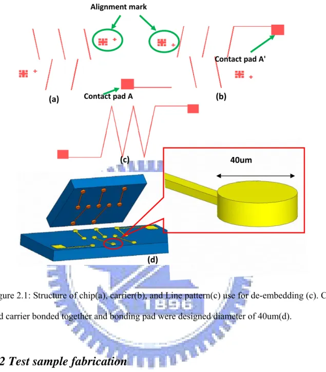
The structure of bonding test sample is shown in Fig. 2.1, respectively. Ten corresponding bonding pads with complementary conducting lines are both designed on two separated carrier Fig. 2.1(a) and chip Fig. 2.1(b). Two alignment marks are set both on carrier and chip for flip chip bonding system during the bonding alignment. The bonding pads, wires and contact pads are fabricated by electro plating copper for 5um and covered with electroless plating 1um Ni and 0.4um Au. The bonding pads for circular bonding interconnection and the diameter of bonding pad is 40um as
shown in Fig. 2.1(d) can be calculated for required bonding pressure. Total length of wires is about 1100um which were designed appropriately for convenience of electrical resistance measurement. Thus, the total contact resistance can be obtained by subtracting the resistance of line pattern (Fig. 2.1(c)) from the resistance measured from two contact pads, A and A’, once carrier and chip are bonded.
6
Alignment mark
Figure 2.1: Structure of chip(a), carrier(b), and Line pattern(c) use for de-embedding (c). Chip and carrier bonded together and bonding pad were designed diameter of 40um(d).
2.2 Test sample fabrication
The fabrication process of test sample is depicted in Fig. 2.2. First, a 0.7um thick SiO2 was deposited onto a P-type (100) silicon substrate by wet oxidation as shown in Fig. 2.2(a). Secondly DC sputtered Ti/Cu 300A/1200A onto oxide as seed layer as shown in Fig. 2.2(b). Then patterned AZ 4620 photo resist to define the region of copper wires and bonding pads as shown in Fig. 2.2(c). The wires and contact pads were fabricated by copper electroplating for 5um as shown in Fig. 2.2(d) and remove photo resist as shown in Fig. 2.2(d). 7
40um Contact pad A (a) (b) (c) Contact pad A' (d) 7
8 um s Fina in F patte Sulf Hyd inor gold spin coate ally, remov Fig. 2.2(g) erned cop furic Acid drogen Pe rganic con d surface, ed AZ 462 ve the pho ). Finally pper layer, d and Hy eroxide s ntamination strong rin 20 PR agai oto resist a electroles , which is ydrogen P solution f n from the se in DI w in to defin and seed l ss plating s to protec Peroxide for severa e gold sur water is req ne bonding layer by A Ni/Au 1 ct all the mixture c al minute face. To p quired afte g pad as sh Acetone an um/0.4um copper w cleaning p es to rem prevent any er this clea hown in F nd CR-7T m to cover ires and p process. A move org y ion rema aning step Fig. 2.2(e). as shown r all the pads from Acid and ganic and ain on the p. . n e m d d e Figur
2.3
Sulf rema re 2.2: TestClean pr
The Au furic Acid ains at 80sample fabbrication proocess.
rocess
surface c d and Hydr which ℃ cleaning p rogen Per is in the f process is roxide in t first step o accompli the ratio of RCA cl ished by u 3:1 and h lean, is co using a m heating the ompatible mixture of e solution to CMOS f n S
MEMs technology. Then dip the wafer into mixed Sulfuric Acid and Hydrogen Peroxide solution for several minutes to remove organic and inorganic contamination from the gold surface. To prevent any ion remain on the gold surface, strong rinse in DI water is required after this cleaning step.
2.4 Flip chip bonding process
A carrier on the sample tray is picked up and set onto the heat stage, then a selected chip flipped over so that the backside surface can be held by upper heater. The two-sight camera is inserted between the chip and carrier. Move and rotate the stage to fit the alignment mark on both side were overlapped. Retract the camera as long as the alignment operation is complete. The upper stage heated at set temperature and move down to exert specific pressure. Usually, bonding time is set within 180 seconds. As the clean process performed on Au bonding pads thermal compressive bonding process should be performed in few minutes due to gold surface may absorb organic substance when exposed to the atmosphere.
9
Chapter 3 Result and discussion
Test sample was fabricated by steps as above, several measurements were set up and done. XPS analysis to identify Au content on bonding pads after cleaning, bonding pressure condition to find minimum pressure requirement, SEM picture of Au-Au bonding adhesion test and cross section are included, contact resistance measurement and AFM analysis shown as below.
3.1 HDXPS Analysis
Au surface contamination is always concerned in thermocompression bonding process. It is believe that the higher surface cleanness improved, the higher bonding strength can be achieved. Since there is not formed significant oxide film on gold at room temperature, and solubility of oxygen, carbon, and hydrogen in gold are all negligibly small, it is believed that gold absorbed organic substance when exposed to the atmosphere [10]. To examine the effectiveness of surface cleaning by Sulfuric Acid and Hydrogen Peroxide mixed solution, XPS analysis was performed on Au surface is shown in Fig. 3.1. It can be seen that after 240 seconds dipping into Sulfuric Acid and Hydrogen Peroxide mixed solution, the content of Au increase from 41.9% to 75.6% and organic contamination, such as carbon or oxygen decrease from Au surface. Compare with cleaning by Ar/H2 plasma after 1 minuite treatment, surface content of Au increased from 37.5% to 80.5% [9].
10
0 5 10 15 20 25 30 35 40 0 10 20 30 40 50 60 70 80 90 0 100 200 300 400 500 C‐PC O‐PC Au‐PC C‐SAB O‐SAB Au‐SAB
Piranha Clean time (s) SAB Clean Time (min)
Surface
Content(%)
Figure 3.1: XPS Content analysis of bonding surface by Sulfuric Acid and Hydrogen Peroxide mixed treatment and compared with SAB process[9].
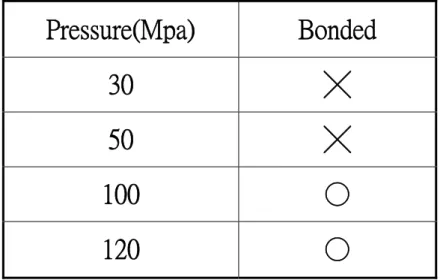
3.2 Bonding pressure condition
XPS analysis shows that Sulfuric Acid and Hydrogen Peroxide mixed cleaned after 240 seconds, Au contents rise up to 70%, which we chose as our typical clean time. To examine the failure mode of 40um Au bump, the test were carried out after bonding under the condition of different pressure. It was found that higher pressure bonding pressure lead chip to be bond after cleaning. In Tab. 3.2, chip and carrier bonded at 160℃, the minimum pressure requirement in this experiment is 100Mpa.
11
Pressure(Mpa)
Bonded
30
╳
50
╳
100
○
120
○
Table 3.2: Pressure condition (○-bonded, ╳-fail)
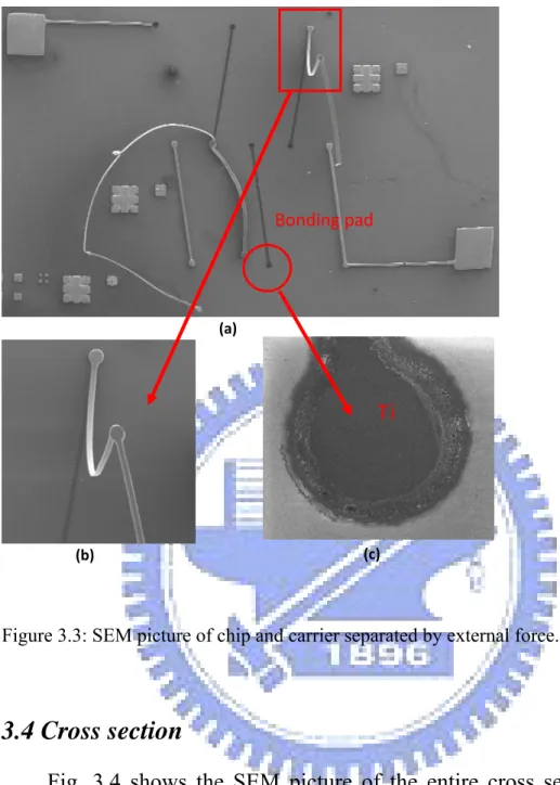
3.3 Au-Au bonding adhesion test
Fig. 3.3 shows the SEM picture of chip and carrier forcefully separated bonding transition structure in the bonding condition of 160 100Mpa for℃ 180 seconds. We know that failure occurs at the weakest region of bonded interface. In Fig. 3.3(a), copper wires and bonding pads on carrier were lifted by exerting external force as the carrier and chip are bonded together. Bonding pads were bonded tightly enough to lift off copper wire from carrier as the detail part of SEM picture shown in Fig. 3.3(b). In Fig. 3.3(c), shows the detail SEM image of lifted off bonding pad. By using EDX analysis, sputtered Ti seed layer adhere on carrier after separation. As the result, we found out that the sputtered Ti/Cu interface is the weakest region to be broken. We have discovered that by using mixture of Sulfuric Acid and Hydrogen Peroxide clean, bonding strength is strong enough to break the interface between Cu and Ti.
12
Figure 3.3: SEM picture of chip and carrier separated by external force.
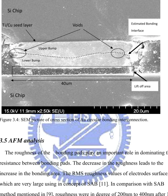
3.4 Cross section
Fig. 3.4 shows the SEM picture of the entire cross section image of the bonding area in the condition of 160 , 100Mpa, 180 secon℃ ds. The upper and lower bump were connect together with high accuracy and no damage was found at interface. There is a lift off area between Si carrier and lower bump, was filled with broken pieces during polish process without unferfilling. As shown in figure, Several voids are found at both right and left ends of the bonding interface as the result of bump deformation under high pressure. These voids may cause contact resistance increases.
(a) Ti Bonding pad (c) (b) 13
Figure 3.4: SEM picture of cross section of Au circular bonding interconnection.
3.5 AFM analysis
The roughness of the bonding pads play an important role in dominating the resistance between bonding pads. The decrease in the roughness leads to the increase in the bonding area. The RMS roughness values of electrodes surface, which are very large using in concept of SAB [11]. In comparison with SAB method mentioned in [9], roughness were in degree of 200nm to 400nm after 10 minutes treatment, By using mixture of Sulfuric Acid and Hydrogen Peroxide clean, RMS roughness was measured at 50nm as shown in Fig 3.5, would supply a good bonding surface to bond with lower contact resistance.
Upper Bump Lower Bump Si Chip Si Chip Voids Estimated Bonding Interface Ti/Cu seed layer 40um Lift off area 14
Figure 3.5: AFM roughness measurement.
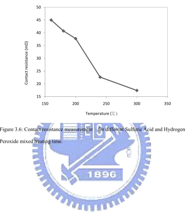
3.6 Contact resistance measurement
The contact resistance of each bonding pad can be derived by dividing the total resistance by the total number of bonding pads. The effect of different bonding temperature on electrical resistance is shown in Fig 3.6. Under the bonding condition of 100MPa, cleaned for 240 seconds, bonding temperature increased from 160℃ to 300℃, the contact resistance decreased from 45 to 17mΩ. The higher temperature applied on the contact area during the bonding process, the more Au surface can be welded, and contact area between the electrodes is greatly increased, the more resistance is decreased.
15
15 20 25 30 35 40 45 50 150 200 250 300 350 Temperature (℃) Contact resistance (m Ω )
Figure 3.6: Contact resistance measurement for different Sulfuric Acid and Hydrogen Peroxide mixed treating time.
16
Chapter 4 Conclusion and Future Work
4.1 Conclusion
We successfully demonstrate a cheaper Au surface clean process for Low temperature thermocompression bonding technology. By piranha clean for 240 seconds interconnection can be bonded in condition of 160℃, 100Mpa.
4.2 Future Work
How to improve piranha clean reliability is the main issue in this work. There is a super piranha clean mentioned in [12]. By using super piranha clean can lower the contact angle on Au surface and reach higher surface energy.
17
References
[1] International Technology Roadmap of Semiconductor,
http://www.itrs.net/Links/2008ITRS/Home2008.htm
[2] Pascariu, G.; Cronin, P.; Crowley, D., "Next generation electronics packaging utilizing flip chip technology," Electronics Manufacturing Technology Symposium, 2003. IEMT 2003. IEEE/CPMT/SEMI 28th International , vol., no., pp. 423-426, 16-18 July 2003
[3] Wu, J.D.; Lee, C.W.; Zheng, P.J.; Li, S., "Effects of substrate metallization on the degradation of flip chip interconnects under electromigration," Advanced Packaging Materials: Processes, Properties and Interfaces, 2004. Proceedings. 9th International Symposium on , vol., no., pp. 25-30, 2004 [4] Ruhmer, K.; Laine, E.; Hauck, K.; Manessis, D.; Ostmann, A.; Toepper,
M., "Low Cost UBM for Lead Free Solder Bumping with C4NP," High Density packaging and Microsystem Integration, 2007. HDP '07. International Symposium on , vol., no., pp.1-7, 26-28 June 2007
[5] Shigetou, A.; Itoh, T.; Matsuo, M.; Hayasaka, N.; Okumura, K.; Suga, T., "Bumpless interconnect through ultrafine Cu electrodes by means of surface-activated bonding (SAB) method," Advanced Packaging, IEEE Transactions on , vol.29, no.2, pp. 218-226, May 2006
[6] Fiedler, S.; Zwanzig, M.; Schmidt, R.; Auerswald, E.; Klein, M.; Scheel, W.; Reichl, H., "Evaluation of Metallic Nano-Lawn Structures for Application in Microelectronic Packaging," Electronics Systemintegration Technology Conference, 2006. 1st , vol.2, no., pp.886-891, Sept. 2006 [7] R, F. Tylecote, The Solid Phase Welding of Materials. New York: St.
Martin's 1968
18
[8] Jae-Woong Nah; Kyung-Wook Paik, "Investigation of flip chip under bump metallization systems of Cu pads," Components and Packaging Technologies, IEEE Transactions on , vol.25, no.1, pp.32-37, Mar 2002 [9] Su-Tsai Lu “A New Approach to Low-Temperature Bonding for Fine
Pitch Chip-on-Flex Technology”, IEEE, Electronics Packaging Technology Conference, pp. 426-432. 2004.
[10] Jellison, James L., "Effect of Surface Contamination on the Thermocompression Bondability of Gold", IEEE Transactions on Parts, Hybrids, and Packaging, Vol. 11, No.3(1975), pp. 206-211.
[11] Takagi, H., Maeda, R., Hisida, N., and Suga, T., “Effect of Surface Roughness on Room-Temperature Wafer Bonding by Ar Beam Surface Activation”, Japan J. Appl. Phys., 1998, p4197-4203.
[12] Hyegeun Min, Ji-Won Park, Hyun Kyong Shon , Dae Won Moon, Tae Geol Lee,“ToF-SIMS study on the cleaning methods of Au surface and their effects on the reproducibility of self-assembled monolayers” Applied surface Science 255 (2008) 1025-1028. 2008.
19
20
![Figure 3.1: XPS Content analysis of bonding surface by Sulfuric Acid and Hydrogen Peroxide mixed treatment and compared with SAB process[9]](https://thumb-ap.123doks.com/thumbv2/9libinfo/7759689.149322/19.892.132.798.118.857/figure-content-analysis-sulfuric-hydrogen-peroxide-treatment-compared.webp)