Optical and electrical transport properties of facing-target sputtered Al doped ZnO
transparent film
Z. Q. Li, D. X. Zhang, and J. J. Lin
Citation: Journal of Applied Physics 99, 124906 (2006); doi: 10.1063/1.2204827 View online: http://dx.doi.org/10.1063/1.2204827
View Table of Contents: http://scitation.aip.org/content/aip/journal/jap/99/12?ver=pdfcov Published by the AIP Publishing
Articles you may be interested in
High-temperature stability of postgrowth-annealed Al-doped MgxZn1-xO films without the phase separation effect
J. Vac. Sci. Technol. B 30, 061201 (2012); 10.1116/1.4754813
Growth morphology and electrical/optical properties of Al-doped ZnO thin films grown by atomic layer deposition J. Vac. Sci. Technol. A 30, 021202 (2012); 10.1116/1.3687939
Effect of substrate temperature on the properties of transparent conductive ZnO:Al thin films prepared by RF sputtering
J. Vac. Sci. Technol. A 29, 051506 (2011); 10.1116/1.3610175
Improved optical and electrical properties of rf sputtered Al doped ZnO films on polymer substrates by low-damage processesa)
J. Vac. Sci. Technol. A 27, 352 (2009); 10.1116/1.3081966
Structural, electrical, and optical properties of transparent conductive oxide ZnO:Al films prepared by dc magnetron reactive sputtering
J. Vac. Sci. Technol. A 19, 963 (2001); 10.1116/1.1368836
Optical and electrical transport properties of facing-target sputtered
Al doped ZnO transparent film
Z. Q. Lia兲
Institute of Advanced Materials Physics, Faculty of Science, Tianjin University, Tianjin 300072, People’s Republic of China
D. X. Zhang
College of Information Technical Science, Nankai University, Tianjin 300071, People’s Republic of China
J. J. Lin
Institute of Physics, National Chiao Tung University, Hsinchu 30010, Taiwan and Department of Electrophysics, National Chiao Tung University, Hsinchu 30010, Taiwan
共Received 29 December 2005; accepted 15 April 2006; published online 22 June 2006兲
Al doped zinc oxide thin film was prepared by dc facing-target sputtering method and its structural, optical, and electrical transport properties have been investigated. The average transmittance of the films is greater than 90% in the wavelength region of 450– 700 nm while the resistivity is as high as 3⫻10−3 ⍀ cm. The band gap energy derived from the transmission data is 3.76 eV, which is higher than that of pure ZnO thin film. This band gap growth phenomenon cannot be explained in terms of the Burstein-Moss effect. The resistivity and Hall effect measurements suggest that the interaction between the charge carriers and phonons plays a key role in the electrical transport properties of the film between 60 and 300 K. The film exhibits negative magnetoresistance at low temperatures, which can be well described by a semiempirical expression that takes into account the third order s-d exchange Hamiltonians describing a negative part and a two-band model for positive contribution. © 2006 American Institute of Physics.关DOI:10.1063/1.2204827兴
I. INTRODUCTION
There has been great interest in zinc oxide semiconduc-tor materials lately, as seen from a surge of a good number of relevant publications.1,2 The interest in ZnO is aroused not only by the transparent conducting characteristics of doped ZnO films but also by the prospects in optoelectronic appli-cations due to a direct wide energy gap共Eg= 3.3 eV at room
temperature兲 in this material. Doping of small amounts of IIIA elements, such as Al, Ga, and In, to ZnO results in a marked decrease in the electrical resistivity while, on the other hand, the optical transparency in the visible range of light spectrum remains high. Hence it is important to clarify the conduction mechanisms in the materials, especially in doped ZnO. The temperature dependence of the resistivity and Hall coefficient represents a key element for the under-standing of the conduction mechanisms in the materials. Sur-prisingly, there have been few reports on the temperature behavior of these transport properties in doped ZnO in the literature.3In the present paper, we have prepared several Al doped ZnO films with high optical transparency by a facing-target sputtering method. Systematic electronic transport measurements, including resistivity, magnetoresistance, and Hall effect, were carried out against the temperature in wide temperature ranges.
II. EXPERIMENT
The Al doped ZnO共or ZnO:Al兲 thin films were depos-ited on glass substrate by the standard dc facing-target sput-tering method. Two Al2O3 doped zinc oxide targets were used as the sputtering source. The weight ratio of Al2O3 to ZnO共both were 99.99% pure兲 was 5%. The base pressure of the chamber was better than 3⫻10−6torr and the sputtering was carried out in an argon 共99.999%兲 atmosphere of 3 ⫻10−2 torr. The sample holder was located at a place outside the plasma zone in our dc facing-target sputtering system. Consequently, the substrate was not directly bombarded by the plasma and thus maintained at a relative low temperature during the sputtering process.共The substrate temperature in-creased by about 50 K during sputtering, which was far lower than the increase occurred in the usual dc or rf sput-tering systems.兲 Hence the dc facing-target sputtering method is a better way to deposit transparent conducting oxide films on polymer substrate. The film thickness, deter-mined by a surface profiler 共Dektak, 6 m兲, was 430 nm. Crystal structure and phase characterization were determined by x-ray diffraction 共XRD兲 using Cu K␣ radiation at room temperature. The optical transmittance of the ZnO:Al film was measured in the wavelength range of 300– 800 nm by using an UV-VIS-NIR 共near infrared兲 scanning spectropho-tometer 共Uv-3101 PC, SHIMADZU兲. The resistivity was measured by a standard four-probe ac technique, and the Hall coefficient was measured by the five-contact method. The temperature dependences of the resistivity and magnetoresis-tance were measured using a physical property measurement
a兲Electronic mail: [email protected]
0021-8979/2006/99共12兲/124906/4/$23.00 99, 124906-1 © 2006 American Institute of Physics [This article is copyrighted as indicated in the article. Reuse of AIP content is subject to the terms at: http://scitation.aip.org/termsconditions. Downloaded to ] IP:
system共PPMS-6000, Quantum Design兲. To confirm our data, all measurements were performed on three pieces of samples prepared at different times but under similar deposition con-ditions. We found that the results on all three films were identical within our uncertainties. Thus, in this report we focus our discussion on one film.
III. RESULTS AND DISCUSSION
Figure 1 shows the XRD pattern of the ZnO:Al film. In the 2 range from 20° to 80°, we observed only two peaks located at 34.18° and 72.04°, respectively. Hence the film was single phased with a hexagonal structure characteristic to that of undoped ZnO 共powder-diffraction file No. 80-0074兲. The two peaks at 34.18° and 72.04° correspond to the 共0002兲 and 共0004兲 planes, respectively, of ZnO. The XRD pattern also indicated that the c axis was the preferred orien-tation of the film.
Figure 2 shows the total transmission properties of the ZnO:Al film. The transmittance of the sample varies from 78.7% to 83% in the wavelength region of 400– 800 nm, and the average transmittance is greater than 90% between 450 and 700 nm. This indicates the excellent optical transparency in the visible range of light spectrum for our thin film, which is of crucial importance for optoelectronic applications. Gen-erally, the optical absorption coefficient␣ is defined as4
I = I0exp共−␣d兲, 共1兲
where I is the intensity of transmitted light, I0is the intensity of incident light, and d is the thickness of the thin film. Since the transmittance TR is defined as I / I0, we obtain ␣ from Eq.共1兲,5
␣= −ln TR
d . 共2兲
According to Tauc et al.,6for a given transition,␣and pho-ton energy hcan be related by the expression
␣=A共hv − Eg兲
m/2
h , 共3兲
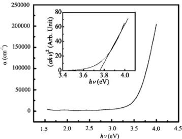
where m = 1 for a direct transition and m = 4 for a indirect transition, Eg is the band gap, and A is a constant. Figure 3
plots the共␣hv兲2against h, from which we obtain the value of the band gap Eg= 3.76 eV, which is higher than that of
pure ZnO thin film 共3.25–3.28 eV兲. Some other authors7 have also observed the band gap growth phenomenon in the Al doped ZnO, but the physical origins causing such an in-crease are still not clarified. It is generally believed that the Burstein-Moss effect7plays a key role in this phenomenon: ZnO is a natural n-type material and the Fermi level would move into the conduction band when it is doped with Al. Since the states below Fermi level in the conduction band are filled, the absorption edge should shift to higher energies. If the Fermi level indeed shifts into the conduction band, the Al doped ZnO should reveal metallic characteristics as that in Sn-doped indium oxide.8 Recently, Imai et al.9 have calcu-lated the electronic band structure of doped and undoped ZnO using density functional theory under the local density approximation. They found that the shape of the density of states curve and the band structure of doped and undoped ZnO are similar to each other, i.e., a semiconductor-to-metal transition does not occur in this system with increasing dop-ing concentration of Al. Experimentally, Gabás et al.10have measured the valence-band spectra of pure ZnO and Al doped 共1% and 3% Al concentrations兲 ZnO films, but they found no samples revealing any density of states around the Fermi level. Hence the Fermi level of the Al doped ZnO does not locate inside the conduction band. Physically, the band gap growth effect in the Al doped ZnO system may originate from the change in the nature and the strength of the inter-action potentials between donors and the host crystals.
FIG. 1. X-ray diffraction pattern of the sample at room temperature.
FIG. 2. Room temperature optical transmission spectra of the Al doped ZnO thin film on glass substrate.
FIG. 3. Plot of absorption coefficient␣with photon energy hfor the Al doped ZnO thin film. Inset: plot of共␣h兲2against photon energy h.
124906-2 Li, Zhang, and Lin J. Appl. Phys. 99, 124906共2006兲
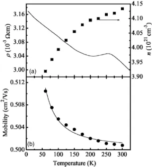
Figure 4 shows a plot of the variations of the resistivity
, charge carrier concentration n, and carrier mobilitywith temperature for the ZnO:Al film. The charge carrier concen-tration is deduced from
RH= −
1
ne, 共4兲
where RHis the Hall coefficient and e is the absolute value of
the electron charge. In our sample, the Hall coefficient is negative at all measuring temperatures, which confirms the
n-type characteristic of the Al doped ZnO film. The carrier
mobility was determined using the relation
= 1
ne. 共5兲
Generally, two scattering mechanisms should be considered in a semiconductor, i.e., scattering by phonons and by ion-ized impurities. At higher temperatures, the interaction be-tween the charge carriers and phonons dominates and the temperature behavior of the carrier mobility共related to lattice scattering兲 can be written as3
L= ALT−3/2, 共6兲
where AL is a coefficient related to the effective mass of
charge carrier. We have performed least-squares fits of our experimental data with the form =0+L, where 0 is a constant. Our best fit关the solid curve in Fig. 4共b兲兴 is obtained with the values for the adjusting parameters 0 = 0.5003 cm2/ V s and A
L= 4.976 cm2K3/2/ V s. The good
agreement between the experiment and theory suggests that the collisions of the conduction electrons with lattice phonons are the dominant scattering process in our sample between 60 and 300 K. The temperature dependence of re-sistivity, shown in Fig. 4共a兲, does not reveal any metallic characteristic, which strongly implies that the Fermi level of
the Al doped ZnO does not locate inside the conduction band. Another important feature of our sample is the small variation in the magnitude of resistivity between the wide temperature range of 2 – 325 K, which should benefit the de-vice fabrication for applications.
Figure 5 shows the magnetic field dependence of the magnetoresistance,⌬/0, at several temperatures between 5 and 30 K. This figure clearly indicates that the magnetore-sistance is negative and its absolute value decreases with increasing temperature at a given magnetic field. Generally, two effects can lead to negative magnetoresistance in non-magnetic materials. The first one is the weak-localization effect11 which originates from coherent backscattering of two, time-reversed, partial electron wave amplitudes, which traverse a closed loop and returned to the origin within a timescale of. The second effect originates from localized magnetic moment.12 It has been proposed that some elec-trons could be localized at the donor sites giving rise to a localized magnetic moment due to statistical fluctuations in donor density and the correlation effects.12 If the weak-localization effect plays a key role in our film, the dephasing timecan be extracted by fitting the low-field magnetore-sistance data with three-dimensional weak-localization theo-retical predictions. However, we found that the weak-localization theory11 cannot describe our magnetoresistance data. On the other hand, our data can be fitted with the semi-empirical expression proposed by Khosla and Fischer:12
⌬/0= − a2ln共1 + b2B2兲 + c2B2/共1 + d2B2兲. 共7兲 The first term in Eq. 共7兲 was obtained by considering the third order of the s-d exchange Hamiltonian. Here the pa-rameters a and b are given by
a2= A1JF关S共S + 1兲 + 具M2典兴 共8兲 and b2=
冋
1 + 4S22冉
2J g冊
4册
g22 共␣kT兲2, 共9兲where J is the exchange integral,Fis the density of states at
the Fermi energy, g is the g factor,具M典 is the average mag-netization, S is the spin of the localized magnetic moment, and␣is a numerical constant. A1is regarded to be a measure of spin based scattering. The second term in Eq.共7兲 describes
FIG. 4.共a兲 Resistivity 共兲 and charge carrier concentration 共n兲 as a function of temperature;共b兲 temperature dependence of carrier mobility 共兲 between 50 and 300 K. The solid line is the least-squares fit to Eq.共6兲.
FIG. 5. 共Color online兲 Magnetoresistance as a function of magnetic field at several temperatures as indicated. The solid lines are the least-squares fits to Eq.共7兲.
a positive component of the magnetoresistance, and it can be deduced from a two-band model by solving the Boltzmann equation.13The parameters c and d are related to the conduc-tivity and relaxation time of each group of carriers. The solid lines in Fig. 5 are the least-squares fits to our magnetoresis-tance共MR兲 data using Eq. 共7兲. This figure clearly indicates that our experimental data are well described by Eq. 共7兲, implying that the negative MR can be explained by the lo-calized magnetic moment model when the third order of the
s-d exchange Hamiltonian is considered. Table I lists the
values of the fitting parameters at different measurement temperatures. As expected, the parameter a shows tempera-ture independent characteristic and b is nearly linear with
T−1, which is consistent with the model. Since the parameters
c and d are related to the magnitude of the positive MR, their
decrease with increasing temperature is reasonable.12
IV. SUMMARY
We have measured the optical and electrical transport properties of an Al doped zinc oxide thin film fabricated by dc facing-target sputtering method. Our film shows excellent optical transparency in the visible range of light spectrum and its resistivity varies weakly with temperature over a wide temperature range of 5 – 330 K. We found that the band gap
energy of the Al doped zinc oxide thin film is greater than that of pure ZnO thin film. This growth in band gap is as-cribed to the change in the nature and strength of the inter-action potentials between donors and the host crystals. The resistivity and Hall effect measurements indicate that the in-teraction between the charge carriers and phonons plays a key role in the electrical transport properties of the film be-tween 60 and 300 K. We have also observed negative mag-netoresistance in the sample at low temperatures and ex-plained the behavior with a semiempirical expression which takes into account the third order s-d exchange Hamiltonians describing a negative part and a two-band model for the positive contribution.
ACKNOWLEDGMENTS
This work is supported by the Natural Science Founda-tion of Tianjin City 共Contract No. 04360211 兲 and National Natural Science Foundation of China 共Nos. 10504024 and 50401002兲.
1Ü. Özgür et al., J. Appl. Phys. 98, 041301共2005兲.
2S. J. Pearton, D. P. Norton, K. Ip, Y. W. Heo, and T. Steiner, Prog. Mater.
Sci. 50, 293共2005兲.
3C. Calderón, G. Gordillo, and J. Olarte, Phys. Status Solidi B 242, 1915
共2005兲.
4K. H. Kim, K. C. Park, and D. Y. Ma, J. Appl. Phys. 81, 7764共1997兲. 5G. K. Paul and S. K. Sen, Mater. Lett. 57, 959共2002兲.
6J. Tauc, R. Grigorvici, and Y. Yanca, Phys. Status Solidi 15, 627共1966兲. 7F. K. Shan and Y. S. Yu, J. Eur. Ceram. Soc. 24, 1869共2004兲. 8Z. Q. Li and J. J. Lin, J. Appl. Phys. 96, 5918共2004兲.
9Y. Imai, A. Watanabe, and I. Shimono, J. Mater. Sci.: Mater. Electron. 14,
149共2003兲.
10M. Gabás, S. Gota, J. R. Ramos-Barrado, M. Sánchez, N. T. Barrett, J.
Avila, and M. Sacchi, Appl. Phys. Lett. 86, 042104共2005兲.
11C. Y. Wu and J. J. Lin, Phys. Rev. B 50, 385共1994兲. 12R. P. Khosla and J. R. Fischer, Phys. Rev. B 2, 4084共1970兲.
13E. H. Sondheimer and A. H. Wilson, Proc. R. Soc. London, Ser. A 190,
435共1947兲. TABLE I. Values of the parameters a, b, c, and d obtained from
least-squares fits to the experimental data.
T共K兲 a b c d 5 0.029 43 8.015 31 0.119 45 3.110 24 10 0.029 46 5.787 99 0.097 23 2.580 46 15 0.028 79 4.351 36 0.079 08 2.247 86 20 0.029 57 2.807 01 0.053 89 1.569 17 25 0.028 92 2.225 02 0.042 19 1.326 42
124906-4 Li, Zhang, and Lin J. Appl. Phys. 99, 124906共2006兲