國 立 交 通 大 學
電子工程學系 電子研究所
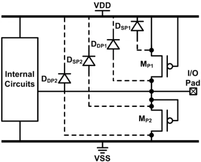
博 士 論 文
射頻電路與高速輸入輸出界面電路
之靜電放電防護設計
ON-CHIP ESD PROTECTION DESIGNS FOR
RADIO-FREQUENCY INTEGRATED
CIRCUITS AND HIGH-SPEED I/O INTERFACE
CIRCUITS
研 究 生:蕭 淵 文 (Yuan-Wen Hsiao)
指導教授:柯 明 道 (Ming-Dou Ker)
射頻電路與高速輸入輸出界面電路
之靜電放電防護設計
ON-CHIP ESD PROTECTION DESIGNS FOR
RADIO-FREQUENCY INTEGRATED
CIRCUITS AND HIGH-SPEED I/O INTERFACE
CIRCUITS
研 究 生:蕭淵文
Student: Yuan-Wen Hsiao
指導教授:柯明道
Advisor: Ming-Dou Ker
國 立 交 通 大 學
電子工程學系 電子研究所
博 士 論 文
A Dissertation
Submitted to Department of Electronics Engineering
and Institute of Electronics
College of Electrical and Computer Engineering
National Chiao Tung University
in Partial Fulfillment of the Requirements
for the Degree of Doctor of Philosophy
in
Electronic Engineering
September 2008
Hsinchu, Taiwan, Republic of China
射頻電路與高速輸入輸出界面電路
之靜電放電防護設計
研究生:蕭淵文
指導教授:柯明道 博士
國立交通大學電子工程學系電子研究所
摘要
隨著近年來通訊技術與積體電路製程的持續演進,無線與有線通訊裝置已經成為生 活中不可或缺的重要設備。藉由無線通訊傳輸資料,使用者可更機動地收發各種訊息, 此演進大幅提昇了資料傳輸的方便性。有線傳輸技術的發展,加速無線接取點與伺服器 間的資料傳輸速度。積體電路製程技術的發展,降低了無線與有線通訊裝置的製造成 本,更激起使用者對通訊裝置的需求與使用意願。 所有電子產品,包含積體電路產品,必須於量產時符合可靠度的規範,以便讓使用 者用得安心,並提供該產品足夠的耐用年限。靜電放電(Electrostatic Discharge, ESD)是 積體電路可靠度中最重要的一環,大多數電子產品的故障與損壞均與遭受靜電放電轟擊 有關。為對積體電路提供有效的靜電放電防護,所有積體電路與外界接觸的銲墊(Pad) 皆須搭配靜電放電防護設計,包含電源銲墊與輸入輸出銲墊,而輸入輸出銲墊上的靜電 放電防護電路會在訊號路徑上產生寄生效應。無線通訊裝置中的射頻(Radio- Frequency, RF)前端電路,亦需要搭配靜電放電防護設計,因為他們連接射頻收發機與外接之濾波 器或天線。由於射頻電路的工作頻段高達數GHz 至數十 GHz,如此高頻的工作頻率對 於訊號路徑上的寄生效應有極嚴格的限制,若訊號路徑上的寄生效應過大,將導致射頻 電路性能的嚴重衰減。除了無線通訊之前端電路,有線傳輸系統中的前端電路,近年來 也在新型傳輸標準中提昇其傳輸速率,故有線傳輸系統中的輸入輸出界面電路對訊號路 徑上的寄生效應要求也日趨嚴格。以上情況引發射頻電路與高速輸入輸出界面電路之靜ii -電放電防護設計的挑戰:如何在最低程度性能衰減的前提下達成最高的靜電放電耐受 度,亦即如何將靜電放電防護元件的寄生效應最小化。 除此之外,互補式金氧半製程的演進,更進一步提昇靜電放電防護設計的困難度。 對核心電路性能而言,使用先進的積體電路製程,電晶體的工作頻率可以提昇,並可降 低元件的雜訊、功率損耗。隨著積體電路製程的進步,電晶體的元件尺寸可以大幅微縮, 故可整合更多電路功能於單一晶片內,此舉開啟了系統單晶片(System on Chip, SoC)的 應用。然而靜電放電轟擊的強度並未隨著積體電路元件微縮而降低,隨著積體電路製程 的演進,電晶體閘極氧化層的崩潰電壓逐漸降低,使電晶體愈容易遭受靜電放電轟擊而 損壞,因此另一個挑戰隨之產生:如何在先進製程中降低靜電放電轟擊時於靜電放電防 護元件上產生的跨壓,以有效保護內部電路。上述兩個挑戰為本論文的研究動機,本論 文由積體電路周圍的銲墊設計開始,循序漸進至積體電路內部的全晶片靜電放電防護設 計與射頻前端電路設計;由單一晶片的電路設計,延伸至整個電子系統的電路板層級元 件充電模式(Board-Level Charged Device Model)靜電放電防護探討。本論文的研究方向 包括:(1)分析目前已發表的射頻電路與高速輸入輸出界面電路之靜電放電防護設計相 關文獻、(2)超低寄生電容的銲墊設計、(3)寬頻分散式放大器之靜電放電防護設計、(4) 搭配全晶片靜電放電防護設計之差動式低雜訊放大器(Low-Noise Amplifier, LNA)、(5) 高速輸入輸出界面電路之靜電放電防護設計、(6)電路板層級元件充電模式靜電放電 (Board-Level Charged-Device-Model ESD)對積體電路產品之影響。
本論文第二章針對目前已發表的射頻電路與高速輸入輸出界面電路之靜電放電防 護設計進行分析,將各種設計分門別類,並歸納各種設計的優缺點與成效。本章首先以 量測結果說明靜電放電防護元件的寄生效應,並闡述靜電放電防護元件對電路性能造成 之負面影響。除寄生效應外,靜電放電防護元件於積體電路遭受靜電放電轟擊時的元件 特性亦相當重要,因為這關係該積體電路的靜電放電耐受度。本章將目前已發表的射頻 電路與高速輸入輸出界面電路之靜電放電防護設計分為三種方式,第一種為使用電路技 巧降低靜電放電防護元件寄生效應的設計方式,使用電路技巧,可將靜電放電防護元件 的寄生效應透過阻抗匹配或阻抗隔絕的方式大幅降低,但額外的元件可能提高晶片面積 或製作成本。第二種方式藉由改變元件佈局以降低靜電放電防護元件的寄生效應,雖然 寄生效應的改善幅度較使用電路技巧的方式小,但由於不需外加元件,故晶片面積與製 作成本亦小於使用電路技巧的方式。第三種方式藉由改變製程降低靜電放電防護元件的 寄生效應,改變半導體的摻雜濃度,可改變接面的寄生電容值,此法雖可以最直觀的方
式降低靜電放電防護元件的寄生效應,但改變製程的可能性在一般應用中並不常見。本 章後段比較各種設計的複雜度、改善後之寄生效應、靜電放電耐受度、與面積使用效率。 除了靜電放電防護元件以外,銲墊也會在訊號路徑上對射頻訊號造成負面影響,為 了提昇射頻電路之性能,銲墊的寄生電容值也必須盡量降低。本論文第三章提出一種新 型具有超低電容值的銲墊架構,可於一般互補式金氧半製程中實現,不需修改製程。在 此新型銲墊架構中藉由使用電感,可抵銷銲墊本身的寄生電容值,以大幅降低整個銲墊 的等效寄生電容值。本研究於130 奈米互補式金氧半製程中實現三種新型設計,分別在 傳統銲墊的區域中,以一層、三層、五層金屬實現三種電感,故此新型設計不需增加銲 墊面積。藉由不同電感值,可產生不同共振頻率,也可達成不同程度的銲墊電容改善量。 實驗結果顯示,藉由銲墊下方電感產生的共振效應,等效銲墊電容可於特定頻段內大幅 降低。以五層金屬實現電感的銲墊架構,在4.3 GHz 至 4.8 GHz 的頻段內,等效銲墊電 容值可降低至接近0 fF。利用此新型銲墊架構,將可降低因傳統銲墊電容造成的訊號延 遲與訊號損耗,進而提昇射頻電路性能。 本論文第四章提出新型分散式靜電放電防護架構,並將其應用於寬頻分散式放大 器,且以0.25 微米互補式金氧半製程實現。當所有靜電放電防護元件的總電容為 300 fF 時,搭配傳統等尺寸式分散式靜電放電防護架構的分散式放大器,其人體放電模式 (Human Body Model, HBM)與機械放電模式(Machine Model, MM)靜電放電耐受度分別 為5.5 kV 與 325 V,且於 1 GHz 至 10 GHz 的頻段內擁有 4.7 ± 1 dB 的增益;搭配新型 遞減尺寸式分散式靜電放電防護架構的分散式放大器,人體放電模式與機械放電模式靜 電放電耐受度可大幅提昇至8 kV 與 575 V,且於 1 GHz 至 9.2 GHz 的頻段內擁有 4.9 ± 1.1 dB 的增益。這兩種分散式靜電放電防護架構均可與分散式放大器共同設計,以達成符 合要求的射頻性能與靜電放電耐受度。 除了搭配靜電放電防護設計的寬頻射頻前端電路外,本論文第五章提出窄頻射頻前 端電路與靜電放電防護電路的共同設計。本章使用130 奈米互補式金氧半製程設計一個 工作於 5 GHz 的差動式低雜訊放大器,並將數種新型靜電放電防護架構應用至該差動 式低雜訊放大器。本研究為目前相關研究中,率先探討差動式低雜訊放大器接點對接點 (Pin to Pin)靜電放電耐受度的研究。所有差動式低雜訊放大器的功率消耗皆為 10.3 mW。沒有搭配靜電放電防護設計的差動式低雜訊放大器,在 5 GHz 的功率增益與雜訊 指數分別為16.2 dB 與 2.16 dB。本章亦實現傳統雙二極體(Double Diode)靜電放電防護 架構的差動式低雜訊放大器,此設計於各輸入銲墊至電源線與接地線間分別放置靜電放
iv -電防護二極體,其人體放電模式與機械放電模式靜電放電耐受度分別為 2.5 kV 與 200 V,在 5 GHz 的功率增益與雜訊指數分別為 17.9 dB 與 2.43 dB。第一個新提出的靜電放 電防護設計使用雙矽控整流器(Silicon-Controlled Rectifier, SCR),此設計於各輸入銲墊 至電源線與接地線間分別放置矽控整流器提供靜電放電防護功能,其人體放電模式與機 械放電模式靜電放電耐受度分別為6.5 kV 與 500 V,搭配此設計的差動式低雜訊放大器 在5 GHz 的功率增益與雜訊指數分別為 17.9 dB 與 2.54 dB。第二個新提出的靜電放電 防護設計於兩個差動輸入銲墊間插入靜電放電匯流排(ESD Bus),藉此於兩個差動輸入 銲墊間提供有效的靜電放電路徑,其人體放電模式與機械放電模式靜電放電耐受度分別 為3 kV 與 100 V,搭配此設計的差動式低雜訊放大器在 5 GHz 的功率增益與雜訊指數 分別為18 dB 與 2.62 dB。第三個新提出的靜電放電防護設計於兩個差動輸入銲墊間使 用交叉耦合(Cross Couple)的矽控整流器,除了可提供單一輸入銲墊至電源線與接地線的 靜電放電防護外,更可在不增加元件的情況下,額外提供兩個差動輸入銲墊間的接點對 接點模式靜電放電防護功能,其此設計的人體放電模式與機械放電模式靜電放電耐受度 分別為1.5 kV 與 150 V,搭配此設計的差動式低雜訊放大器在 5 GHz 的功率增益與雜訊 指數分別為19.2 dB 與 3.21 dB。另一個靜電放電防護設計搭配雙二極體與交叉耦合矽控 整流器,可達成4 kV 人體放電模式與 300 V 機械放電模式的靜電放電耐受度,搭配此 設計的差動式低雜訊放大器在5 GHz 的功率增益與雜訊指數分別為 19.1 dB 與 3.05 dB。 除了比較靜電放電耐受度外,搭配各種靜電放電防護設計的差動式低雜訊放大器之射頻 性能,亦於第五章內比較與討論。 本論文第六章提出高速輸入輸出界面電路之靜電放電防護設計。首先量測在 130 奈米互補式金氧半製程中P 型擴散區與 N 井接面(P+/N-well)及 N 型擴散區與 P 井接面 (N+/P-well)兩種二極體在不同尺寸下的靜電放電耐受度與寄生電容值。為了確保能提供 一般商用規範的2 kV 人體放電模式靜電放電耐受度,靜電放電防護二極體需使用 40 微
米以上的周長實現。接著利用仿製接收級電晶體(Dummy Receiver NMOS)架構,將電晶 體的閘極連接至輸入銲墊,並將電晶體的汲極、源極、基底接地,搭配選定之靜電放電 防護二極體尺寸與電源箝制靜電放電防護電路,可量測此仿製接收級電晶體的靜電放電 耐受度。由於仿製接收級電晶體的連接方式近似於一般接收級內電晶體的連接方式,故 可由仿製電晶體的靜電放電耐受度推估一般接收級的靜電放電耐受度。此靜電放電防護 設計亦應用至2.5 GHz 的高速接收級界面電路,在 250 fF 寄生電容的限制下,此靜電放 電防護設計可達成3 kV 的人體放電模式靜電放電耐受度。此外本論文第六章提出一種
新型設計,將原本置於輸入銲墊與接地線間的 N 型擴散區與 P 井接面(N+/P-well)二極 體置換為矽控整流器,藉由與電源箝制靜電放電防護電路共用靜電放電偵測電路,輸入 輸出接點的寄生電容可有效降低,並可藉由使用矽控整流器提昇靜電放電耐受度。本研 究將靜電放電防護元件與部分靜電放電偵測電路置於輸入銲墊下方,可節省晶片面積, 並降低訊號路徑上的寄生電容值。 完成單一積體電路晶片的靜電放電防護設計後,每個晶片皆須安裝至電子產品的模 組內並進行功能測試,此時可能引發電路板層級元件充電模式靜電放電,導致晶片損 毀。本論文第七章探討電路板層級元件充電模式靜電放電對積體電路產品造成的威脅, 首先簡介晶片層級與電路板層級元件充電模式靜電放電的成因,並說明數個積體電路晶 片遭受電路板層級元件充電模式靜電放電損壞的實例。由於電路板層級元件充電模式靜 電放電的電流峰值與電子模組中的電路板尺寸有密切關係,第七章第二部分量測不同電 路板尺寸所產生的電路板層級元件充電模式靜電放電電流波形,實驗結果顯示較大的電 路板尺寸或將電路板充電至較高電壓,將導致較大的電路板層級元件充電模式靜電放電 電流峰值,為了降低此電流峰值,以免損壞模組內的積體電路晶片,在放電路徑上可放 置串聯電阻,實驗結果顯示此舉可大幅降低電路板層級元件充電模式靜電放電的電流峰 值。第七章亦對數個以互補式金氧半製程製作的測試元件與測試電路進行晶片層級與電 路板層級元件充電模式靜電放電測試,測試結果發現電路板層級元件充電模式靜電放電 耐受度較低,且造成較嚴重的損壞情形,故電路板層級元件充電模式靜電放電對積體電 路晶片的威脅比晶片層級元件充電模式靜電放電更為嚴重。 第八章總結本論文的研究成果,並提出數個接續本論文研究方向的研究題目。由於 目前對電路板層級的靜電放電測試方式尚未有明確規範,本論文於附錄提出「積體電路 之電路板層級元件充電模式靜電放電測試標準」提案,提案中詳細定義電路板層級靜電 放電測試的各項測試條件與量測方式。 本論文所提出的各項新型設計,均搭配實驗晶片量測結果以驗證設計之理論,且有 相對應的國際期刊與國際研討會論文發表。本論文中數個創新設計已提出專利申請。
-ON-CHIP ESD PROTECTION DESIGNS FOR
RADIO-FREQUENCY INTEGRATED CIRCUITS AND
HIGH-SPEED I/O INTERFACE CIRCUITS
Student: Yuan-Wen Hsiao Advisor: Dr. Ming-Dou Ker
Department of Electronics Engineering and Institute of Electronics
National Chiao-Tung University
Abstract
With the continuous evolution of communication technology and integrated circuit (IC) process, wireless and wireline communication devices had become essential in daily life. By using the wireless communication devices to transmit data, users can access any information more conveniently. Advance wireline communication technology speedups the data transmission rate between the access points (AP) and the server. The continuous scaling of IC process technology further stimulates the demand for communication devices.
All microelectronic products, including IC products, must meet the reliability specifications during mass production in order to be safely used and provide moderate life time. Electrostatic discharge (ESD), which has become one of the most important reliability issues in IC products, must be taken into consideration during the design phase of all IC products. Most of the failures and damages found in ICs were demonstrated to be related to ESD. To provide effective ESD protection for the IC, all pads which connect the IC and the external world need to be equipped with ESD protection circuits, including the input/output (I/O) pads, VDD pads, and VSS pads. However, the ESD protection devices at the I/O pads inevitably cause parasitic effects on the signal path. The radio-frequency (RF) front-end circuits in wireless communication devices need ESD protection design as well because they connect the RF transceiver to the external antenna or band-select filter. Since the RF
front-end circuits operate in the frequency band ranging from several gigahertzes to tens of gigahertz, such a high operating frequency leads to strict limitations for the parasitic effects on the signal path. If the parasitic effects on the signal path are too large, RF circuit performance will be seriously degraded. Besides RF front-end circuits, the data rates of recent wireline communication standards also increase, so the parasitic effects on the signal paths of high-speed I/O interface circuits in wireline communication systems also need to be watched. The situation introduces the challenge in ESD protection design for RF circuits and high-speed I/O interface circuits, which is to achieve the highest ESD robustness with the smallest performance degradation. In other words, the parasitic effects of the ESD protection devices need to be minimized.
Furthermore, the evolution of CMOS process increases the difficulty of ESD protection design. Advanced CMOS technologies not only increase the operating frequency of transistors but also reduce the noise of active devices and power consumption. With the continuous scaling of CMOS technology, the dimensions of CMOS devices are reduced, so more function blocks can be integrated into a single chip. This is the application of system on chip (SoC). However, ESD was not scaled down with the CMOS technology. MOS transistors fabricated in advanced CMOS processes have thinner gate oxide and thus lower gate-oxide breakdown voltage, so they are more vulnerable to ESD. Here comes the other design challenge, which is to reduce the voltage across the ESD protection devices under ESD stresses in advanced CMOS processes. The two aforementioned design challenges form the motivation of this dissertation. This dissertation begins at the design in the periphery of the IC, which is the bond pad, and enters the co-design of RF front-end and ESD protection circuits. Besides, this dissertation covers the whole-chip ESD protection design within a single chip and the investigation of board-level charged-device-model (CDM) ESD issue in IC products. The research topics including: (1) overview of previous works on ESD protection design for RF and high-speed I/O interface circuits, (2) ultra low-capacitance bond pad design, (3) ESD protection design for wideband distributed amplifier, (4) differential low-noise amplifier (LNA) with whole-chip ESD protection design, (5) ESD protection design for high-speed I/O interface circuits, and (6) investigation on board-level CDM ESD issue in IC products.
In chapter 2, the published ESD protection designs for RF front-end circuits and high-speed interface circuits are overviewed. The designs are categorized with their individual advantages and disadvantages clearly analyzed. The RF performance degradation caused by ESD protection devices are illustrated with measured results. Besides, the
characteristics of ESD protection devices under ESD stress conditions are quite important, because it determines the ESD robustness. The designs are categorized into three groups, which are the circuit solution, layout solution, and process solution. With the circuit technique, the impacts of parasitic effects caused by ESD protection devices on circuit performance can be significantly mitigated by impedance matching or impedance isolation. However, the increased chip area due to the extra components increases the fabrication cost. With the layout modification, the parasitic effects and dimensions of ESD protection devices can be moderately reduced. Since no extra component is used, the fabrication cost is lower than that with circuit technique. The third group is process modification. By modifying the doping concentration, the junction capacitance can be adjusted to reduce the parasitic effects of ESD protection devices. However, process modification is uncommon in general IC products. The design complexity, improved parasitic effect, ESD robustness, and area efficiency of all reported designs are compared in this chapter.
Besides ESD protection devices, bond pads also cause impacts on circuit performance because of their parasitic capacitance. To mitigate the performance degradation, bond-pad capacitance needs to be minimized as well. A new low-capacitance bond pad structure in CMOS technology for RF applications is proposed in chapter 3. Three kinds of inductors stacked under the pad are used in the proposed bond pad structure. Experimental results in a 130-nm CMOS process have verified that the bond-pad capacitance is reduced due to the cancellation effect provided by the inductor embedded in the proposed bond pad structure. The bond-pad capacitance is reduced to almost 0 fF from 4.3 to 4.8 GHz. The proposed bond pad structure is fully compatible to general CMOS processes without any extra process modification.
In chapter 4, two distributed ESD protection schemes are proposed and applied to protect distributed amplifiers against ESD stresses. Fabricated in a 0.25-μm CMOS process, the distributed amplifier with the first protection scheme of the equal-sized distributed ESD (ES-DESD) protection scheme, contributing an extra 300 fF parasitic capacitance to the circuit, can sustain the human-body model (HBM) ESD level of 5.5 kV and machine-model (MM) ESD level of 325 V, while exhibits the flat-gain of 4.7 ± 1 dB from1 to 10 GHz. With the same total parasitic capacitance, the distributed amplifier with the second protection scheme of the decreasing-sized distributed ESD (DS-DESD) protection scheme achieves better ESD robustness, where the HBM ESD level is over 8 kV and MM ESD level is 575 V, and has the flat-gain of 4.9 ± 1.1 dB over the 1 to 9.2-GHz band. With these two proposed ESD protection schemes, the wideband RF performances and high ESD robustness of the
distributed amplifier can be successfully co-designed to meet the application specifications. Besides ESD protection design for wideband RF frond-end circuits, co-design of narrow band LNA and ESD protection circuit is proposed in chapter 5. A 5-GHz differential LNA is implemented in a 130-nm CMOS process, and several new ESD protection schemes are applied to this differential LNA. This is the first work which investigates the pin-to-pin ESD robustness of differential LNAs. All of the fabricated differential LNAs consume 10.3 mW from the 1.2-V power supply. The reference differential LNA without ESD protection has 16.2-dB power gain and 2.16-dB noise figure at 5 GHz. The conventional double-diode ESD protection scheme is realized for the differential LNA, which has 2.5-kV HBM and 200-V MM ESD robustness. The differential LNA with the double-diode ESD protection scheme has 17.9-dB power gain and 2.43-dB noise figure at 5 GHz. With the proposed double silicon-controlled rectifier (SCR) ESD protection scheme, the HBM and MM ESD levels are significantly improved to 6.5 kV and 500 V, respectively. Besides, the differential LNA with the double-SCR ESD protection has 17.9-dB power gain, and 2.54-dB noise figure at 5 GHz. Another proposed design uses an ESD bus between the differential input pads, which has 3-kV HBM and 100-V MM ESD robustness. The differential LNA with the proposed ESD bus has 18-dB power gain and 2.62-dB noise figure at 5 GHz. The ESD protection design using cross-coupled SCR devices between the differential input pads is also proposed. Besides providing ESD protection for a single input pad, pin-to-pin ESD protection is also achieved without adding any extra devices. This ESD protection scheme achieves 1.5-kV HBM and 150-V MM ESD levels, respectively. The power gain and noise figure of this differential LNA are 19.2 dB and 3.2 dB, respectively. By using other diodes beside the cross-coupled SCR devices, the turn-on efficiency of ESD protection devices can be enhanced. With the double diodes and the cross-coupled SCR devices, the ESD-protected differential LNA achieves 4-kV HBM and 300-V MM ESD robustness, and exhibits 19.1-dB power gain and 3-dB noise figure at 5 GHz.
Chapter 6 presents the ESD protection design for high-speed I/O interface circuits. The ESD levels and parasitic capacitances of P+/N-well and N+/P-well ESD protection diodes with different dimensions are characterized in the beginning. Then the double-diode ESD protection scheme is applied to the dummy receiver NMOS and the dummy transmitter NMOS. Since the connection of the dummy receiver NMOS (dummy transmitter NMOS) is similar to that of the NMOS transistor in a receiver (transmitter) interface circuit, the ESD robustness of the dummy receiver NMOS (dummy transmitter NMOS) can be used to predict the ESD robustness of the high-speed interface circuit with this ESD protection scheme. This
whole-chip ESD protection scheme is also applied to a 2.5-Gb/s high-speed I/O interface circuit, and the ESD robustness is larger than 3 kV in HBM with the parasitic capacitance of less than 250 fF. Moreover, a new ESD protection scheme is proposed in chapter 6. By replacing the N+/P-well diode between the input pad and VSS with the SCR, the ESD robustness can be further improved. In the ESD protection schemes in chapter 6, the ESD protection devices and part of the ESD detection circuit is placed under the I/O pad to reduce the chip area and the parasitic capacitance on the signal path.
After finishing ESD protection design for a single chip, the chip needs to be installed in a module and module function test will be performed. At this time, board-level CDM ESD events may occur to damage the ICs. In chapter 7, the impacts caused by board-level CDM ESD events on IC products are investigated. The mechanism of board-level CDM ESD event is introduced first. Based on this mechanism, an experiment has been performed to investigate the board-level CDM ESD current waveforms under different sizes of printed circuit boards (PCBs), different charged voltages, and different series resistances in the discharging path. Experimental results have shown that the discharging current strongly depends on the PCB size, charged voltage, and series resistance. Moreover, chip-level and board-level CDM ESD levels of several test devices and test circuits fabricated in CMOS processes have been characterized and compared. Test results have shown that the board-level CDM ESD level of the test circuit is lower than the chip-level CDM ESD level, which demonstrates that the board-level CDM ESD event is more critical than the chip-level CDM ESD event. In addition, failure analysis reveals that the failure on the test circuit under the board-level CDM ESD test is much severer than that under the chip-level CDM ESD test.
Chapter concludes the achievement in this dissertation, and suggests several future works in this field. Since the standard for the board-level CDM ESD test is not established so far, the proposal of the “Test standard for board-level charged-device-model electrostatic discharge robustness of integrated circuits” (in Chinese) is presented in the appendix. In the proposal, the test methodology and test conditions are clearly defined.
In this dissertation, several novel designs have been proposed in the aforementioned research topics. Measured results of fabricated test chips have demonstrated the performance improvement. The achievements of this dissertation have been published in several international journal and conference papers. Several innovative designs have been applied for patents.
Acknowledgment
在交通大學電子研究所的碩博士班生涯中,首先感謝恩師柯明道教授四
年多年來的耐心指導與鼓勵,讓我順利完成博士學業。除了專業領域上的
訓練,柯教授認真且積極的研究態度與明快且嚴謹的處事原則,讓我學得
如何快速解決問題、有效率地處理各項事務、並交出高水準成果的正確態
度與方式。作研究的過程雖然辛苦且伴隨無數大小挫折,但培養的能力將
造就無可取代的價值。柯教授為研究群同學爭取的許多福利,更讓人感念
在心。
感 謝 交 通 大 學 吳 重 雨 校 長 、 美 國 伊 利 諾 大 學 香 檳 校 區 的
Elyse
Rosenbaum 教授、晶焱科技姜信欽博士、中山大學王朝欽教授、閎康科技
謝詠芬博士、臺灣大學王暉教授、交通大學蘇朝琴教授在百忙之中抽空擔
任我的口試委員,並給予珍貴的指導與建議,讓此博士論文更加完整。
感謝任職於聯華電子的唐天浩先生、王暢資先生,與任職於智原科技的
曾玉光博士、蔡富義博士、黃俊先生鼎力協助實驗晶片下線與研究工作進
行,也感謝任職於閎康科技的黃志國先生協助靜電放電耐受度量測,使本
論文的研究成果得以成功驗證,並順利發表於國際期刊與國際研討會。
感謝李健銘學長與郭秉捷學長開創射頻電路之靜電放電防護設計的研
究領域,傳承過去的研究成果,大幅縮短摸索的時間,也加速本研究的順
利進行。感謝實驗室的前輩施育全博士、徐國鈞博士、林昆賢博士、陳世
倫博士、許勝福博士、陳榮昇博士、張瑋仁博士、羅文裕學長、王文傑學
長、陳世宏學長、顏承正學長、陳穩義學長、吳偉琳學姊
、陳志豪學長、
黃鈞正學長、黃祖德學長、陳勝豪學長、陳旻珓
學長、
盧台祐學長、
與賴
泰翔、王資閔、林群祐、莊介堯、邱柏硯等同學與學弟們在研究與生活上
的協助與扶持。此外,感謝實驗室助理卓慧貞小姐在行政事務上的許多協
助。
由衷感謝敬愛的父親蕭國順先生、母親呂禎鈴女士、姊姊蕭淑仁小姐、
哥哥蕭淵云先生。感謝親人的支持、陪伴與照顧,讓我順利完成學業。感
謝女友陳香菱小姐,一路走來無悔的相伴。感謝所有幫助我、陪伴我一同
成長的師長、朋友、學長姊、同學、學弟妹們,願大家平安喜樂。
蕭 淵 文
誌於竹塹交大
九十七年 夏
Contents
Abstract (Chinese)
i
Abstract (English)
vii
Acknowledgment
xiii
Contents
xv
Table Captions
xxi
Figure Captions
xxiii
1. Introduction
1
1.1. Background of ESD Protection Design for High-Frequency I/O Interfaces 1
1.1.1. Standards of Commercial Wireless and Wireline Communications 6
1.1.2. Considerations of ESD Protection Design for Radio-Frequency (RF) Front-End Circuits and High-Speed I/O Interface Circuits 7
1.2. Board-Level Charged-Device-Model (CDM) ESD Issue 11
1.3. Organization of This Dissertation 13
2. Overview on ESD Protection Design for Radio-Frequency/High-Speed
I/O Interfaces
17
2.1. Trade-Off Between ESD Robustness and High-Frequency Circuit Performance 17
2.2. ESD Protection Designs by Circuit Solutions 19
2.2.1. Stacked ESD Protection Devices 19
2.2.2. Impedance Cancellation Technique 20
2.2.3. Impedance Isolation Technique 23
2.2.4. Series LC Resonator 24
2.2.5. Impedance Matching 26
2.2.6. Inductive ESD Protection 29
2.2.7. T-Coil 30
2.2.8. Distributed ESD Protection 32
2.2.10. Substrate-Triggering Technique 37
2.3. ESD Protection Designs by Layout Solutions 40
2.3.1. Low-Capacitance Layout Structure for MOSFET 40 2.3.2. Low-Capacitance Layout Structure for SCR 41 2.3.3. Waffle Layout Structure 44 2.3.4. ESD Protection Device Under I/O Pad 45
2.4. ESD Protection Designs by Process Solutions 48
2.4.1. Symmetrical SCR Structure 48
2.4.2. Low-Capacitance MOSFET 49
2.5. Discussion and Comparison 50 2.6. Summary 52
3. Ultra Low-Capacitance Bond Pad for Radio-Frequency Applications in
CMOS Technology
53
3.1. Background 53 3.2. Proposed Ultra Low-Capacitance Bond Pad 54 3.3. Equivalent Circuit Model for the Proposed Bond Pad 57 3.4. Experimental Results and Discussion 58
3.4.1. Extracted Bond-Pad Capacitance 59 3.4.2. Extracted Bond-Pad Insertion Loss 60 3.4.3. Comparison Among Simulated and Measured Results 63
3.5. Summary 64
4. ESD Protection Design for 1-to-10 GHz Distributed Amplifier in CMOS
Technology
65
4.1. Background 65 4.2. Distributed Amplifier Design 67
4.2.1. Basic Distributed Amplifier Structure 67
4.2.2. Ideal Distributed Amplifier 69
4.2.3. Inductor Modeling 70
4.2.4. Optimized Distributed Amplifier 72
4.3. ESD Protection Design for Distributed Amplifier 74
4.3.2. Proposed Distributed ESD Protection Schemes 75 4.3.3. Simulated RF Performance of Distributed Amplifier Without
and With ESD Protection 76
4.4. Experimental Results 80
4.4.1. Measured Wideband RF Performance 81
4.4.2. ESD Robustness 85
4.4.3. Failure Analysis 86
4.5. Summary 87
5. 5-GHz Differential Low-Noise Amplifier With High Pin-to-Pin ESD
Robustness in CMOS Technology
89
5.1. Background 90 5.2. Differential LNA Design 92 5.3. ESD Protection Design for Differential LNA 95
5.3.1. Substrate-Triggered Silicon-Controlled Rectifier (SCR) 95 5.3.2. Power-Rail ESD Clamp Circuit With SCR 98 5.3.3. Conventional Double-Diode ESD Protection Scheme 99 5.3.4. Proposed Double-SCR ESD Protection Scheme 100 5.3.5. Proposed ESD Protection Design With ESD Bus 101 5.3.6. Proposed ESD Protection Design With Cross-Coupled SCR 102 5.3.7. Simulated RF Performance of LNA Without and With ESD Protection 105
5.4. Experimental Results 108 5.4.1 Measured RF Performance 108
5.4.2 ESD Robustness 113
5.4.3 Failure Analysis 117
5.5. Discussions and Design Guidelines 118
5.6. Summary 120
6. ESD Protection Design for High-Speed I/O Interface Circuits in CMOS
Technology
121
6.1. Background 121 6.2. ESD Protection Diodes 122 6.3. Whole-Chip ESD Protection Design 127
6.3.1. ESD Protection Design With Dummy Receiver NMOS 129 6.3.2. ESD Protection Design With Dummy Transmitter NMOS 130 6.3.3. ESD Levels of Dummy Receiver NMOS
and Dummy Transmitter NMOS 131
6.4. ESD-Protected 2.5-Gb/s High-Speed I/O Interface Circuit 132 6.5. Discussions and Design Guidelines 137
6.6. Summary 137
7. Investigation on Board-Level Charged-Device-Model ESD Issue in IC
Products
139
7.1. Background 139 7.2. CDM ESD Events 140
7.2.1. Chip-Level CDM ESD Event 141
7.2.2. Case Study on Chip-Level CDM ESD Damage 142
7.2.3. Board-Level CDM ESD Event 144
7.3. Dependence of Current Waveforms on the Board Size in Board-Level CDM ESD Event 148
7.3.1. Discharging Without Series Resistor 148 7.3.2. Discharging With Series Resistor 151
7.4. Verifications With Test Devices and Test Circuits 152
7.4.1. Test With Gate-Grounded NMOS 154 7.4.2. Test With Dummy Receiver NMOS 155 7.4.3. Test With 2.5-GHz High-Speed Receiver Interface Circuit 156
7.5. Summary 157
8. Conclusions
and
Future
Works
161
8.1 Main Results of This Dissertation 161 8.2 Future Works 164
Appendix: Proposal of “Test Standard for Board-Level Charged-Device-
References
173
Vita
185
Table Captions
Chapter 1
Table 1.1. Allocated Frequency Bands of the Wireless Communication Standards 6 Table 1.2. Data Rates of the Wireline Communication Standards 7
Chapter 2
Table 2.1. Comparison Among the ESD Protection Designs for RF Front-End Circuits and High-Speed I/O Interface Circuits 51
Chapter 3
Table 3.1 Dimensions of Passive Components Used in the Bond-Pad Model With 5-Layer
Stacked Inductor 63
Chapter 4
Table 4.1 Parasitic Capacitance in Each ESD Protection Section of the ESD-Protected
Distributed Amplifiers 77
Table 4.2 HBM and MM ESD Robustness of the Distributed Amplifiers 85 Table 4.3 Comparison With Prior CMOS Distributed Amplifiers 86
Chapter 5
Table 5.1 ESD Protection Scheme of Each Differential LNA 100 Table 5.2 HBM and MM ESD Robustness of the Differential LNAs 114 Table 5.3 Comparison With Prior CMOS Differential LNAs 118
Chapter 6
Table 6.1 Characteristics of ESD Protection Diodes in a 130-nm CMOS Process 125 Table 6.2 ESD Robustness of Dummy Receiver NMOS (RX_NMOS) and Dummy
Transmitter NMOS (TX_NMOS) With Different Dimensions of ESD Protection
Diodes 132
Table 6.3 ESD Protection Design of Each High-Speed Receiver Interface Circuit 133 Table 6.4 HBM ESD Robustness of the High-Speed Receiver Interface Circuits 136
Chapter 7
Table 7.1 Measured Results on Chip-Level CDM and Board-Level CDM ESD Robustness of Dummy Receiver NMOS (RX_NMOS) 156 Table 7.2 Measured Chip-Level CDM ESD Robustness of 2.5-Gb/s High-Speed Receiver
Interface Circuit 158
Table 7.3 Measured Board-Level CDM ESD Robustness of 2.5-Gb/s High-Speed receiver
Figure Captions
Chapter 1
Fig. 1.1. Equivalent circuits of (a) HBM and (b) MM ESD tests. 2 Fig. 1.2. Whole-chip ESD protection scheme for ICs 2 Fig. 1.3. Four ESD-test pin combinations for the IC products: (a) positive-to-VSS mode (PS-mode), (b) negative-to-VSS mode (NS-mode), (c) positive-to-VDD (PD-mode), and (d) negative-to-VDD (ND-mode). 3 Fig. 1.4. Pin combinations in pin-to-pin ESD tests: (a) positive mode, and (b) negative
mode. 3
Fig. 1.5. Pin combinations in VDD-to-VSS ESD tests: (a) positive mode, and (b) negative
mode. 4
Fig. 1.6. Typical double-diode ESD protection scheme. 4 Fig. 1.7. ESD current paths in the typical double-diode ESD protection scheme under (a) PS-mode ESD stresses, (b) ND-mode ESD stresses, and (c) pin-to-pin ESD
stresses. 5
Fig. 1.8. IC chip with ESD protection devices at the input and output pads. 9 Fig. 1.9. Block diagram of an ESD-protected RF receiver. 10 Fig. 1.10. Block diagram of an LNA with ESD protection circuit. VS, RS, and RL denote the
source voltage, source resistance, and load resistance, respectively. 10 Fig. 1.11. Equivalent circuit of CDM ESD test. 12
Chapter 2
Fig. 2.1. Measured (a) power gains (S21-parameters) and (b) noise figures of STI diodes
with different device dimensions in a 0.25-μm CMOS process. 18 Fig. 2.2. ESD protection design with stacked ESD diodes to reduce the capacitance from I/O pad to ac ground nodes. 20 Fig. 2.3. Simulated S21-parameter of an ideal parallel LC resonator under different
frequencies. 21
Fig. 2.4. ESD protection design with the parallel LC resonator. 22 Fig. 2.5. ESD protection circuit using the impedance-cancellation technique. The inductor LP cancels the parasitic capacitance from ESD protection device and provides
Fig. 2.6. ESD protection design with LC-tanks. 23 Fig. 2.7. ESD protection design with stacked LC-tanks. 24 Fig. 2.8. Simulated S21-parameter of an ideal series LC resonator under different
frequencies. 25
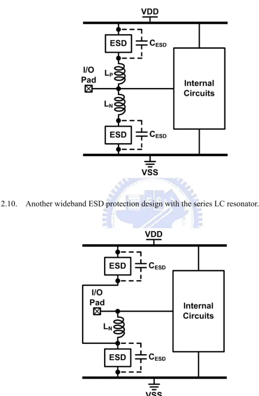
Fig. 2.9. Wideband ESD protection design with the series LC resonator. 25 Fig. 2.10. Another wideband ESD protection design with the series LC resonator. 26 Fig. 2.11. Modified wideband ESD protection design with the series LC resonator. Only an inductor is connected in series with two ESD protection devices. 26 Fig. 2.12. ESD protection design with shunt and series components to achieve impedance
matching. 27
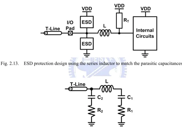
Fig. 2.13. ESD protection design using the series inductor to match the parasitic
capacitances. 28
Fig. 2.14. Small-signal equivalent circuit model of the high-speed I/O interface circuit
shown in Fig. 2.15. 28
Fig. 2.15. ESD protection design with a balun and the impedance matching network. 29 Fig. 2.16. Inductor-based ESD protection design for LNA. 30 Fig. 2.17. Transformer-based ESD protection design for LNA. 30 Fig. 2.18. Wideband ESD protection design with T-coil. 31 Fig. 2.19. Wideband ESD protection with T-diode. 31 Fig. 2.20. Distribute ESD protection scheme. 32 Fig. 2.21. Equal-size distributed ESD (ES-DESD) protection scheme. 33 Fig. 2.22. Decreasing-size distributed ESD (DS-DESD) protection scheme. 33 Fig. 2.23. π-model distributed ESD (π-DESD) protection scheme. 34 Fig. 2.24. Matching loci of (a) ES-DESD, (b) DS-DESD, and (c) π-DESD protection
schemes in the Smith chart. 35
Fig. 2.25. Traditional ESD protection circuit with GDPMOS and GGNMOS. 36 Fig. 2.26. ESD protection circuit with increased reverse-bias voltage to reduce the parasitic
PN-junction capacitance. 36
Fig. 2.27. ESD protection circuit utilizing the unity-gain amplifier to keep the voltage across the parasitic capacitance to zero. 37 Fig. 2.28. ESD protection design with the substrate-triggering circuit to turn on the ESD
protection device. 38
Fig. 2.29. Whole-chip ESD protection scheme with the substrate-triggered SCRs and series
Fig. 2.30. Equivalent circuit of the whole-chip ESD protection scheme of Fig. 2.31. 39 Fig. 2.31. Layout top view of the low-capacitance NMOS transistor. 40 Fig. 2.32. Cross-sectional view of the low-capacitance NMOS transistor. 40 Fig. 2.33. Low-capacitance SCR: (a) Layout top view and (b) cross-sectional view. 42 Fig. 2.34. Cross-sectional view of the modified low-capacitance SCR with STI. 42 Fig. 2.35. ESD protection design with a parasitic SCR: (a) Circuit schematic and (b)
cross-sectional view. 43
Fig. 2.36. P+/N-well waffle diode: (a) Layout top view, and (b) cross-sectional view. 44 Fig. 2.37. Waffle SCR: (a) Layout top view, and (b) cross-sectional view. 45 Fig. 2.38. ESD protection device under the I/O pad proposed in [82]: (a) Layout top view, and (b) schematic circuit diagram. 46 Fig. 2.39. ESD protection device under the I/O pad proposed in [83]: (a) Layout top view, and (b) schematic circuit diagram. 47 Fig. 2.40. ESD protection device with symmetrical SCR: (a) Cross-sectional view, and (b)
schematic circuit diagram. 49
Fig. 2.41. Cross-sectional view of the low-capacitance PMOS proposed in [85]. 50
Chapter 3
Fig. 3.1. (a) Reference bond pad. (b) Proposed bond pad with the 1-layer inductor. (c) Proposed bond pad with the 3-layer stacked inductor. (d) Proposed bond pad with the 5-layer stacked inductor. 55 Fig. 3.2. Basic circuit schematic to illustrate the idea of bond-pad capacitance cancellation.
57 Fig. 3.3. Layout top view of the test pattern to extract the bond-pad capacitance. 57 Fig. 3.4. Equivalent circuit model of the proposed bond pad. 58 Fig. 3.5. Two-port S-parameter measurement setup. 59 Fig. 3.6. Extracted bond-pad capacitances among the fabricated bond pads under different
frequencies. 60
Fig. 3.7. Diagram to shown the bond-pad insertion loss. 61 Fig. 3.8. Two-port network represented by the ABCD matrix. 62 Fig. 3.9. The basic two-port network used to extract the bond-pad insertion loss. 62 Fig. 3.10. Extracted insertion losses of the fabricated bond pads under different frequencies.
62 Fig. 3.11. Comparison of the simulated and extracted bond-pad capacitance. 63
Chapter 4
Fig. 4.1. Basic distributed amplifier. 67
Fig. 4.2. Normalized gain response of the distributed amplifier with different staggering factors. r = 1 corresponds the unstaggered case. 68 Fig. 4.3. Low-pass m-derived half section. 69 Fig. 4.4. Modified distributed amplifier with staggering technique and m-derived half
section. 69
Fig. 4.5. Ideal distributed amplifier according to the design theorems. 70 Fig. 4.6. Simulated S-parameters of the ideal distributed amplifier shown in Fig. 4.5. 70 Fig. 4.7. Simulated phase shift of S21-parameter of the ideal distributed amplifier shown in
Fig. 4.5. 71
Fig. 4.8. Frequency-dependent π-model for on-chip inductors. 71 Fig. 4.9. Comparison of inductance between the lumped π-model and the simulated spiral
inductor. 72
Fig. 4.10. Arbitrarily optimized distributed amplifier. 72
Fig. 4.11. Feasible distributed amplifier. 73
Fig. 4.12. Comparison of S21-parameters among the feasible distributed amplifier, the
arbitrarily optimized distributed amplifier, and the distributed amplifier with ideal
inductors. 74
Fig. 4.13. Distributed amplifier with distributed ESD protection scheme. 75 Fig. 4.14. Resistive ladder model of the distributed ESD protection scheme during ESD
stresses. 76
Fig. 4.15. Simulated S21-parameters of the distributed amplifiers without and with
distributed ESD protection schemes. The total parasitic capacitance of ESD protection devices are 300 fF. 78 Fig. 4.16. Simulated phase shifts of the distributed amplifiers without and with distributed ESD protection schemes. The total parasitic capacitance of ESD protection
devices are 300 fF. 78
Fig. 4.17. Simulated S21-parameters of the distributed amplifiers without and with
distributed ESD protection schemes. The total parasitic capacitance of ESD protection devices are 600 fF. 79 Fig. 4.18. Simulated phase shifts of the distributed amplifiers without and with distributed ESD protection schemes. The total parasitic capacitance of ESD protection
Fig. 4.19. Chip micrograph of the fabricated distributed amplifiers in a 0.25-μm CMOS
process. 80
Fig. 4.20. Measured and simulated S21-parameter of the reference distributed amplifier
without ESD protection (DA0). 81 Fig. 4.21. Measured S21-parameters of the distributed amplifiers with and without ESD
protection. 82
Fig. 4.22. (a) S11-parameters, (b) S22-parameters, and (c) S12-parameters among the
simulated and fabricated distributed amplifiers without ESD protection (DA0), distributed amplifier with the ES-DESD protection scheme (DA1), and distributed amplifier with the DS-DESD protection scheme (DA2). 83 Fig. 4.23. Phase shifts among the simulated and fabricated distributed amplifiers without
ESD protection (DA0), distributed amplifier with the ES-DESD protection scheme (DA1), and distributed amplifier with the DS-DESD protection scheme
(DA2). 84
Fig. 4.24. Noise figures among the simulated and fabricated distributed amplifiers without ESD protection (DA0), distributed amplifier with the ES-DESD protection scheme (DA1), and distributed amplifier with the DS-DESD protection scheme
(DA2). 84
Fig. 4.25. EMMI pictures to show the failure location of ESD damage in the distributed amplifier with the DS-DESD protection scheme (DA2) after PS-mode 575-V MM ESD test. (a) Whole view of DA2. (b) Zoomed-in view of the damaged location at the P+/N-well P-diode1 in the first ESD protection section. 87
Chapter 5
Fig. 5.1. Reference differential LNA (LNA0) without ESD protection. 92 Fig. 5.2. (a) Input network of the ESD-protected LNA. (b) Equivalent input network of the ESD-protected LNA at the operating frequency. 93 Fig. 5.3. (a) Cross-sectional view of P-type substrate-triggered silicon-controlled rectifier (P-STSCR). (b) Equivalent circuit of P-STSCR. 96 Fig. 5.4. (a) Cross-sectional view of N-type substrate-triggered silicon-controlled rectifier
(N-STSCR). (b) Equivalent circuit of N-STSCR. 97 Fig. 5.5. Measured dc I–V curves of the stand-alone SCR device in a 130-nm CMOS process under different temperatures. 98 Fig. 5.6. Power-rail ESD clamp circuit realized with P-STSCR. 99
Fig. 5.7. Differential LNA (LNA1) with the conventional double-diode ESD protection
scheme. 100
Fig. 5.8. Differential LNA (LNA2) with the proposed double-SCR ESD protection scheme. 101 Fig. 5.9. Differential LNA (LNA3) with the proposed ESD bus. 102 Fig. 5.10. Establishing the SCR path between the differential input pads by putting the
P-diode for one input pad and the N-diode for the other input pad together. 103 Fig. 5.11. Differential LNA (LNA4) with the proposed cross-coupled SCR devices. 104 Fig. 5.12. Differential LNA (LNA5) with the proposed cross-coupled SCR devices. 104 Fig. 5.13. Simulated S21-parameters (power gain) of the reference differential LNA (LNA0)
and the five ESD-protected differential LNAs (LNA1–LNA5). 106 Fig. 5.14. Simulated S11-parameters (input reflection) of the reference differential LNA
(LNA0) without ESD protection and the five ESD-protected differential LNAs
(LNA1–LNA5). 106
Fig. 5.15. Simulated S22-parameters (output reflection) of the reference differential LNA
(LNA0) without ESD protection and the five ESD-protected differential LNAs
(LNA1–LNA5). 107
Fig. 5.16. Simulated S12-parameters (reverse isolation) of the reference differential LNA
(LNA0) without ESD protection and the five ESD-protected differential LNAs
(LNA1–LNA5). 107
Fig. 5.17. Simulated noise figures of the reference differential LNA (LNA0) without ESD protection and the five ESD-protected differential LNAs (LNA1–LNA5). 108 Fig. 5.18. Chip micrographs of (a) the reference differential LNA (LNA0) without ESD
protection, and (b) the differential LNA (LNA2) with the proposed double-SCR
ESD protection scheme. 109
Fig. 5.19. Chip micrographs of the reference differential LNA (LNA0) without ESD protection and the five ESD-protected differential LNAs (LNA1–LNA5). 109 Fig. 5.20. Measured S21-parameters (power gain) of the reference differential LNA (LNA0)
and the five ESD-protected differential LNAs (LNA1–LNA5). 110 Fig. 5.21. Measured S11-parameters (input reflection) of the reference differential LNA
(LNA0) without ESD protection and the five ESD-protected differential LNAs
(LNA1–LNA5). 111
Fig. 5.22. Measured S22-parameters (output reflection) of the reference differential LNA
(LNA1–LNA5). 111 Fig. 5.23. Measured S12-parameters (reverse isolation) of the reference differential LNA
(LNA0) without ESD protection and the five ESD-protected differential LNAs
(LNA1–LNA5). 112
Fig. 5.24. Measured noise figures of the reference differential LNA (LNA0) without ESD protection and the five ESD-protected differential LNAs (LNA1–LNA5). 112 Fig. 5.25. ESD current paths under pin-to-pin ESD stress in (a) LNA1 with the conventional double-diode ESD protection scheme, (b) LNA2 with the proposed double-SCR ESD protection scheme, (c) LNA3 with the proposed ESD bus, (d) LNA4 with the proposed cross-coupled SCR, and (e) LNA5 with the double diodes and the
proposed cross-coupled SCR. 116
Fig. 5.26. SEM pictures at the failure points of (a) LNA1 with the double-diode ESD protection scheme after 3-kV HBM pin-to-pin ESD test, and (b) LNA2 with the double-SCR ESD protection scheme after 7-kV HBM PS-mode ESD test. The failure locations are all located at the gate oxide of input NMOS M1. 119
Chapter 6
Fig. 6.1. (a) Layout top view and (b) cross-sectional view of P+/N-well diode. 123 Fig. 6.2. (a) Layout top view and (b) cross-sectional view of N+/P-well diode. 124 Fig. 6.3. (a) Layout top view and (b) cross-sectional view of N-well/P-substrate diode. 124 Fig. 6.4. Extracted parasitic capacitances of (a) P+/N-well diode, (b) N+/P-well diode, and (c) N-well/P-substrate diode in a 130-nm CMOS process. 126 Fig. 6.5. TLP-measured I-V curves of (a) P+/N-well diodes, (b) N+/P-well diodes, and (c) N-well/P-substrate diodes in a 130-nm CMOS process. 128 Fig. 6.6. TLP-measured It2 values of ESD protection diodes under different dimensions in
a 130-nm CMOS process. 129
Fig. 6.7. HBM ESD levels of ESD protection diodes under different dimensions in a 130-nm CMOS process. The ESD protection diodes have identical HBM ESD robustness under the same size. 129 Fig. 6.8. Dummy receiver NMOS (RX_NMOS) used as a test circuit to verify the
effectiveness of the proposed ESD protection scheme in a receiver (double diodes and active power-rail ESD clamp circuit). 130 Fig. 6.9. Dummy transmitter NMOS (TX_NMOS) used as a test circuit to verify the
diodes and active power-rail ESD clamp circuit). 131 Fig. 6.10. 2.5-Gb/s high-speed receiver interface circuit with the first whole-chip ESD
protection scheme (Receiver_1–Receiver_2). 133 Fig. 6.11. 2.5-Gb/s high-speed receiver interface circuit with the second whole-chip ESD
protection scheme (Receiver_3–Receiver_8). 134 Fig. 6.12. Layout top view of the ESD protection devices under the bond pad. 135 Fig. 6.13. Cross-sectional view of the ESD protection devices under the bond pad. 135 Fig. 6.14. Measured eye diagram of the 2.5-Gb/s high-speed I/O interface circuit in a
130-nm CMOS process. 137
Chapter 7
Fig. 7.1. CDM ESD event: When a certain pin is grounded, the stored charges in the integrated circuit (IC) will be quickly discharged through the grounded pin. 142 Fig. 7.2. (a) CDM ESD current path in an input buffer. (b) The failure point is located at the gate oxide of the input NMOS. 143 Fig. 7.3. After chip-level CDM ESD test, the failure point is located at the gate oxide of an NMOS in the internal circuit. 144 Fig. 7.4. The charges stored in the printed circuit board (PCB) and the chip will be
redistributed when the chip is attached to the PCB. 145 Fig. 7.5. When two capacitors with different voltages are shorted, charge redistribution will
occur. 145
Fig. 7.6. When a certain pin of the PCB is grounded during function test, huge current will flow from the PCB through the IC. 146 Fig. 7.7. When the driver IC is attached to the LCD panel during manufacturing, the
charges originally stored in the LCD panel will be transferred to the driver IC, which causes board-level CDM ESD event. During panel function test, connecting the pins of the driver IC to ground will also induce the board-level CDM ESD
event. 147
Fig. 7.8. When the pins of the driver IC are grounded, board-level CDM ESD current will flow from the LCD panel through the interface circuits within driver IC to the
grounded pins. 147
Fig. 7.9. ESD protection devices are inserted between different power domains to provide ESD current paths between the separated power domains. 148 Fig. 7.10. Experimental setup to investigate the current waveforms under board-level CDM
ESD events. 149 Fig. 7.11. Measured board-level CDM ESD current waveforms from (a) 1/8-A4-sized PCB and (b) A4-sized PCB under 100-V charged voltage. 150 Fig. 7.12. Measured board-level CDM ESD current waveforms from 1/4-A4-sized PCB
under (a) 20-V and (b) 200-V charged voltage. 150 Fig. 7.13. Board-level CDM ESD peak currents under different charged voltages and
different PCB sizes. 151
Fig. 7.14. Experimental setup to investigate the current waveforms under board-level CDM ESD events with a series resistor along the discharging current path. 152 Fig. 7.15. Measured board-level CDM ESD current waveform of the 1/2-A4-sized PCB with (a) 100-Ω and (b) 10-kΩ series resistances along the discharging path under 100-V
charged voltage. 152
Fig. 7.16. Board-level CDM ESD peak currents under different series resistances. 153 Fig. 7.17. Discharging times of board-level CDM ESD events under different series
resistances. 153
Fig. 7.18. Field-induced chip-level CDM ESD measurement setup. 154 Fig. 7.19. Field-induced board-level CDM ESD measurement setup. 154 Fig. 7.20. Measured current waveforms with gate-grounded NMOS (GGNMOS) under (a)
+1-kV chip-level CDM ESD test, and (b) +1-kV board-level CDM ESD test. 155 Fig. 7.21. Test circuit with dummy receiver NMOS (RX_NMOS) for chip-level and
board-level CDM ESD tests. 156
Fig. 7.22. Scanning-electron-microscope (SEM) pictures of the failure points on the 2.5-Gb/s high-speed receiver interface circuit after (a) -1300-V chip-level CDM ESD test, and (b) -900-V board-level CDM ESD test. 158
Chapter 1
Introduction
In this chapter, the background and the organization of this dissertation are discussed. First, the considerations of electrostatic discharge (ESD) protection design for radio-frequency (RF) front-end circuits and high-speed (input/output) I/O interface circuits in complementary metal-oxide-semiconductor (CMOS) processes are discussed. Secondly, the board-level charged-device-model (CDM) ESD issue of CMOS integrated circuit (IC) products is introduced. Finally, the organization of this dissertation is described.
1.1. Background of ESD Protection Design for High-Frequency
I/O Interfaces
With the advantages of high integration and low cost for mass production, high-frequency (input/output) I/O interfaces operating in gigahertz (GHz) frequency bands have been widely designed and fabricated in CMOS processes. Such high-frequency applications include RF front-end circuit in wireless communications and high-speed I/O interface circuits in wireline communications. Electrostatic discharge (ESD), which has become one of the most important reliability issues in integrated circuit (IC) products, must be taken into consideration during the design phase of all ICs [1]–[4], including the radio-frequency (RF) front-end circuits and high-speed I/O interface circuits. Without ESD protection circuits at all I/O pads, the RF performance of a wireless transceiver can be easily damaged by ESD stresses, because RF front-end circuits are always fabricated in advanced CMOS processes. Usually the I/O pads are connected to the gate terminal of MOS transistor or silicided drain/source terminal, which leads to a very low ESD robustness if no ESD protection design is applied to the I/O pad. Once the RF front-end circuit is damaged by ESD, it can not be recovered and the RF functionality is lost. Besides ESD caused threats to RF front-end circuits, the effects of ESD-induced damage in the high-speed I/O interface circuits had also been studied. It had been demonstrated that the termination resistance of high-speed I/O interface circuits is changed after ESD stresses. The impedance mismatch after ESD
stresses causes significant waveform distortion on the I/O signals, which seriously degrades the performance of high-speed I/O interface circuits [5]. Therefore, on-chip ESD protection circuits must be provided for all I/O pads in ICs. Two common chip-level (or component-level) ESD test standards are human-body-model (HBM) and machine-model (MM) ESD test standards [6], [7]. HBM and MM ESD tests are used to evaluate the ESD robustness of the IC when it is touched by the charged human body or charged machine. The equivalent circuits of HBM and MM ESD tests are shown in Fig. 1.1(a) and (b), respectively. In order to protect the internal circuits against ESD stresses, ESD protection circuits must be provided at all I/O pads. The concept of whole-chip ESD protection design is illustrated in Fig. 1.2.
(a) (b) Fig. 1.1. Equivalent circuits of (a) HBM and (b) MM ESD tests.
Fig. 1.2. Whole-chip ESD protection scheme for ICs.
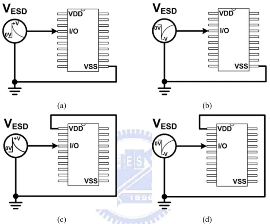
The ESD-test pin combinations are shown in Fig. 1.3. ESD stresses may have positive or negative voltages on an I/O pin with respect to the grounded VDD or VSS pin. The typical
ESD specifications for commercial IC products in HBM and MM are 2 kV and 200 V, respectively. For comprehensive ESD verification, the pin-to-pin ESD stresses and VDD-to-VSS ESD stresses had also been specified to verify the whole-chip ESD robustness, which are shown in Fig. 1.4 and 1.5, respectively.
(a) (b)
(c) (d)
Fig. 1.3. Four ESD-test pin combinations for the IC products: (a) positive-to-VSS mode (PS-mode), (b) negative-to-VSS mode (NS-mode), (c) positive-to-VDD (PD-mode), and (d) negative-to-VDD (ND-mode).
(a) (b)
(a) (b)
Fig. 1.5. Pin combinations in VDD-to-VSS ESD tests: (a) positive mode, and (b) negative mode.
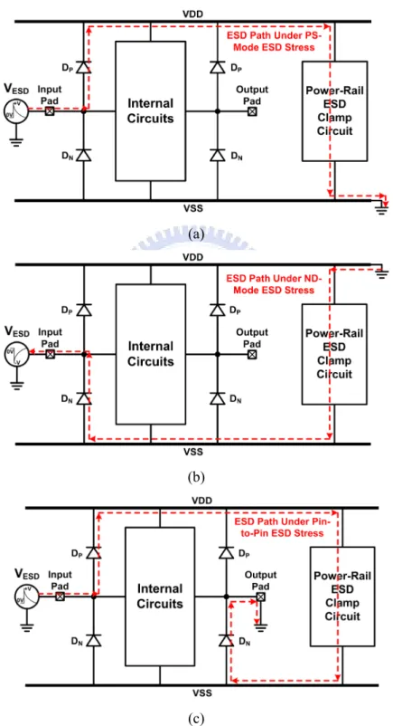
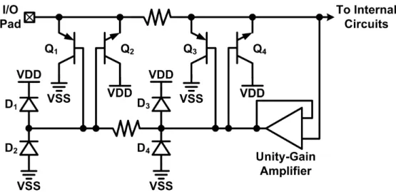
Fig. 1.6 shows the typical on-chip double-diode ESD protection scheme in which two ESD diodes at I/O pad are co-designed with the power-rail ESD clamp circuit to prevent internal circuits from ESD damage [8]. In Fig. 1.6, a P+/N-well diode (DP) and an N+/P-well
diode or an N-well/P-substrate diode (DN) are placed at input pad or output pad. When the DP
and DN are under forward-biased condition, they can provide discharge paths from I/O pad to
VDD and from VSS to I/O pad, respectively.
Fig. 1.6. Typical double-diode ESD protection scheme.
During the positive-to-VDD (PD) mode and negative-to-VSS (NS) mode ESD stresses, ESD current is discharged through the forward-biased DP and DN, respectively. To avoid the
ESD diodes from being operated under breakdown condition during the positive-to-VSS (PS) mode and negative-to-VDD (ND) mode ESD stresses, which results in a substantially lower ESD robustness, the power-rail ESD clamp circuit is used between VDD and VSS to provide ESD current paths between the power rails [9]. Thus, ESD current is discharged from the I/O
pad through the forward-biased DP to VDD, and discharged to the grounded VSS pin through
the turn-on efficient power-rail ESD clamp circuit during PS-mode ESD stresses, as shown in Fig. 1.7(a). Similarly, ESD current is discharged from the VDD pin through the turn-on efficient power-rail ESD clamp circuit and the forward-biased DN to the I/O pad during
ND-mode ESD stresses, as shown in Fig. 1.7(b).
(a)
(b)
(c)
Fig. 1.7. ESD current paths in the typical double-diode ESD protection scheme under (a) PS-mode ESD stresses, (b) ND-mode ESD stresses, and (c) pin-to-pin ESD stresses.
During pin-to-pin ESD stresses, ESD current flows from the zapped I/O pad through the forward-biased DP, the power-rail ESD clamp circuit, and the forward-biased DN to the
grounded I/O pad, as shown in Fig. 1.7(c). Under VDD-to-VSS ESD tests, ESD current flows through the power-rail ESD clamp circuit between VDD and VSS. Since the power-rail ESD clamp circuit works independently between VDD and VSS, its parasitic effects do not have any impact on the internal circuits. With the turn-on efficient power-rail ESD clamp circuit, the ESD diodes can be assured to be operated in the forward-biased condition under all ESD test modes, which leads to higher ESD robustness.
1.1.1. Standards of Commercial Wireless and Wireline Communications
With the evolution of communication technologies, more and more applications become available. To successfully transmit the signals without interfering with other applications in the free space, every wireless communication standard is allocated with some specific frequency bands. Table 1.1 lists the allocated frequency bands of the wireless communication standards. The operating frequency bands ranges from less than 1 GHz to more than 10 GHz. The front-end circuits in the transmitters or receivers are operated at the specified frequency to handle the RF signal. The mixers perform the conversion between the RF signal and the
Table 1.1
Table 1.2
Data Rates of the Wireline Communication Standards
Note: GB/s and Gb/s denote gigabytes per second and gigabits per second, respectively.
baseband signal. Similarly, the standards of the wireline communication standards also specified the maximum data rates of each standard, as listed in Table 1.2. The high-speed I/O interface circuits are used to transmit or receive the high-speed signals between the I/O buses. With the multiplexer (MUX) and demultiplexer (DEMUX), the high-speed signals are transmitted on the I/O buses, while the digital signals are processed in the transceiver. Unfortunately, ESD protection circuits are required to be applied to the I/O pads of the transceiver, including the I/O pads transmitting or receiving the high-speed or RF signals. Thus, ESD protection circuits are required to protect the transceiver against ESD damages without degrading the performance of the transceiver.
1.1.2. Considerations of ESD Protection Design for Radio-Frequency (RF)
Front-End Circuits and High-Speed I/O Interface Circuits
Although using power-rail ESD clamp circuit between VDD and VSS does not cause any effect on the internal circuits, applying ESD protection devices at the I/O pads inevitably introduce some negative impacts to circuit performance due to their parasitic effects. The
main parasitic effect caused by ESD protection devices which deteriorates the high-frequency performance is the parasitic capacitance. Since the input signal swing is small at the RF input pad, it is sensitive to the shunt parasitic capacitance of ESD protection devices. Therefore, the parasitic capacitance of the ESD protection device at the RF input pad is strictly limited. For the RF transmitter, the devices in the output stage are implemented with large dimensions to transmit the output signals with large enough signal power. With proper design, the devices in the RF output stage can be used to protect the RF output pad against ESD stresses. Thus, ESD protection design for the input pad of the RF receiver is more challenging than that for the output pad of the RF transmitter.
A typical request on the maximum loading capacitance of ESD protection device for a 2-GHz RF input pin was specified as only ~200 fF, which includes the parasitic capacitances of bond pad and ESD protection device [10]. Recently, the negative impacts of ESD protection devices to RF circuit performance had been investigated [11], [12], which had demonstrated that the RF performance such as power gain and noise figure are significantly degraded by the parasitic capacitance of ESD protection devices. The impacts become more serious as the operating frequency of RF front-end circuits and high-speed I/O interface circuits increases. Thus, the parasitic capacitance of ESD protection device must be minimized in ESD protection design for high-frequency applications. Generally, ESD protection circuits cause RF performance degradation with several undesired effects, which are will be discussed in the following.
Parasitic capacitance is one of the most important design considerations for RF ICs and high-speed I/O interface circuits operating in gigahertz frequency bands. Conventional ESD protection devices with large dimensions have the parasitic capacitance which is too large to be tolerated for RF front-end circuits. As shown in Fig. 1.8, the parasitic capacitance of ESD protection devices causes signal loss from the pad to ground. Moreover, the parasitic capacitance also changes the input matching condition. Consequently, the noise figure is deteriorated and the power gain is decreased.
Noise figure is one of the most important merits for RF receivers. Since the RF receiver is a cascade of several stages, the overall noise figure of the RF receiver can be obtained in terms of the noise figure and power gain of each stage in the receiver. For example, if there are m stages cascaded in the RF receiver, the total noise figure of the RF receiver can be expressed as [13]