國立交通大學
電信工程學系
碩士論文
應用於超寬頻無線射頻接收機之 CMOS 低雜
訊放大器與混頻器設計與研究
Design of CMOS Low-noise Amplifier and Mixer for UWB
Wireless RF Receiver
研究生:熊子豪
指導教授:周復芳 博士
應用於超寬頻無線射頻接收機之
CMOS 低雜訊放大器與混頻器設
計與研究
Design of CMOS Low-noise Amplifier and Mixer for UWB Wireless
RF Receiver
研究生:熊子豪 Student: Zi.Hao.Hsiung
指導教授:周復芳 博士 Advisor: Dr. Christina F. Jou
國 立 交 通 大 學
電 信 工 程 學 系 碩 士 班
碩 士 論 文
A thesis
Submitted to Department of Communication Engineering College of Electrical and Computer Engineering
National Chiao Tung University In Partial Fulfillment of the Requirements
for the Degree of Master of Science in Communication Engineering
June 2007
Hsinchu, Taiwan, Republic of China
I
應用於超寬頻無線射頻接收機之
CMOS 低雜訊放大器與混頻
器設計與研究
研究生:熊子豪 指導教授:周復芳 博士
國立交通大學電信工程學系碩士班
摘 要
本論文討論應用於超寬頻射頻接收機的高頻電路設計且主要分為兩個主題探 討。其中第ㄧ主題是超寬頻低雜訊放大器的分析和設計。第一主題中:探討兩種 不同類型的低雜訊放大器:低電壓 (0.75 伏特)、低雜訊放大器和電晶體寄生電容 回授式低雜訊放大器。為了達到偏壓於0.75 伏特,電路主體架構選擇褶疊式疊接 組態,量測結果顯示:在供應電壓0.75 V 功率消耗 11 毫瓦的條件下,頻寬 3.1-7.5 GHz 達到 7.5 dB 增益,雜訊指數為 4.8-7.5dB。電容回授式低雜訊放大器,主要利 用低頻的電容回授和高頻的電阻回授形成兩個頻率點匹配,達成超寬頻匹配。量 測結果顯示出:頻寬2.7- 12 GHz,輸入端反射係數皆小於-10dB。3dB 增益頻寬為 1.8-8.3 GHz,功率增益約為 10dB。 第二主題為:摺疊式電流再利用式超寬頻混頻器。此超寬頻混頻器量測結果 顯示使用-10dBm 的本地震盪器,頻寬 3.1-8.1 GHz 的範圍內,在中頻 100MHz, 可 得 到 13.5-15.5dB 的 降 頻 轉 換 功 率 增 益 , -11.5dBm 三 階 諧 波 交 會 點 , 和 11-14.5dB DSB 雜訊指數,主電路功率消耗為 11.3 毫瓦。 最後,一個使用0.18um CMOS 整合型超寬頻前端電路已被模擬,此超寬頻前 端電路也當作此論文的將來專題研究II
Design of CMOS Low-noise Amplifier and Mixer for UWB
Wireless RF Receiver
Student: Zi.Hao.Hsiung Advisor: Dr. Christina F. Jou
Department of Communication Engineering
National Chiao Tung University
ABSTRACT
This thesis discusses high frequency circuit design for ultra wide-band RF receivers and it mainly includes two parts. One is the analysis and design of ultra wide-band LNA. In part one, we discuss two kinds of UWB LNA:Low voltage (0.75 V), low noise amplifier, and wide-band matched LNA design using transistor's intrinsic gate-drain capacitor. Because the supply voltage is low, we choose folded cascode stage for amplifying stage. The measured results reveal that power gain is 7.5 dB, noise figure is 4.8-7.5 dB and power consumption is 11 mW. The capacitor feedback low noise amplifier makes use of capacitor feedback in low frequency mode and resistor feedback in high frequency mode to achieve two matching mechanism to form wide-band matching. The measured results reveal that the S11 is better than -10 dB from 2.75-12 GHz, S21 is about 10 dB and the 3 dB band-with is 1.9-8.3 GHz.
In part two, we demonstrate a folded, current reused UWB mixer in a standard 0.18um CMOS technology. This UWB mixer achieves measured high conversion power gain of 13.5-15.5 dB at IF=100 MHz with -10 dbm LO power, -11.5 dBm IIP3, and 11-14.5 dB of DSB noise figure. The power consumption of core circuit is 11 mW.
III
been simulated. This wide-band RF front end circuit is treated as feature work in our thesis.
IV
致謝
研究所兩年的生活,首先我要感謝我的指導教授周復芳博士,讓我在射頻的領域 能有效率的成長,並對於人生的意義有不一樣的見解。同時要感謝口試委員郭建 男博士及胡政吉博士的不吝指導,使這篇論文更為完善。此外,要特別感謝國家 晶片中心量測課人員在量測上所給予的協助與指導,使我可以精確的量測到晶片 的各項參數。 另外要感謝匯儀學長的教導,指引了我研究方向,讓研究更有目標。還有要感謝 實驗室的同學瑞嫻、智鵬、宇清和怡星,因為有你們陪伴我的碩士生活,使我在 學習成長的路上不曾感到孤單;在此特別感謝智鵬所擁有的個人特色,讓我們實 驗室總是在出奇不意的狀況下沉醉在歡樂的氣份中;也很感謝瑞嫻不時的莫名臉 紅,常惹得實驗室的成員開懷大笑。另外要感謝已畢業的學長文明、仕豪、博揚、 政展、秋榜和宏斌,你們認真的研究態度一直是我的榜樣。也要感謝俊緯學長、 昱舜、志豪等學弟,因為有你們的搞笑,讓我度過愉快的碩二。也感謝老劉這兩 年的陪伴與支持,讓我更有勇氣完成碩士論文。 最後我要感謝我最愛的父母親和姐姐,在求學的路上給予我最大的支持和包容, 讓我能順利地完成碩士學業。在此僅以小小的研究成果貢獻給我家人,並與你們 分享我的喜悅。子豪 於 2007 年 風城 夏
V
CONTENTS
Chinese Abstract I
English Abstract II
Acknowledgement IV
Contents V
List of Tables VII
List of Figures VIII
Chapter 1
Introduction ... 1
-1.1 Background and motivation... - 1 -
1.2 Thesis organization ... - 3 -
Chapter 2
CMOS LowNoise Amplifier for UWB System... 5
-2.1 Introduction... - 5 -
2.2 Ultra Wide-band Low-Noise Amplifier ... - 7 -
2.2.1 Low-voltage, Low noise Ultra-Wideband Amplifier... - 7 -
2.2.1.1 Architectures ... - 7 -
2.2.1.2 Design considerations ... - 9 -
2.2.2 3–8 GHz wideband LNA Using Capacitor Feedback... - 16 -
2.2.2.1 Architectures ... - 16 -
2.2.2.2 Design considerations ... - 17 -
2.3 Chip implementation and measured result... - 20 -
2.4 Comparison and Discussion... - 36 -
Chapter 3
A Folded Current-Reused Mixer for UWB Applications
System ... 38
-3.1 Introduction... - 38 -
3.2 Review of basic mixer ... - 40 -
3.2.1 Basic mixer topology ... - 40 -
3.2.2 Some special mixer topology... - 43 -
3.3 Folded current-reused Ultra-band mixer... - 46 -
3.4 Chip implementation and measured considerations ... - 48 -
3.5 Measurement results and discussion... - 52 -
3.5.1 Measurement results ... - 52 -
VI
Chapter 4
Conclusion and Future Work... 63
-4.1 Conclusion ... - 63 -
4.1.1 Low voltage Ultra Wide-band LNA ... - 63 -
4.1.2 3-8 GHz capacitor feedback Wide-band LNA... - 64 -
4.1.3 Folded Current Reuse Ultra Wide-band Mixer... - 64 -
4.2 Future Work ... - 65 -
Appendix ... 66
-A.1 Traditional Receiver and MBOA Receiver Front End ... - 66 -
A.2 Main Block Description... - 70 -
A.2.1 LNA ... - 70 -
A.2.2 Mixer... - 71 -
A.3 Layout and Simulation Results ... - 72 -
A.3.1 Layout Consideration... - 72 -
A.3.2 Simulation Results ... - 73 -
-VII
LIST
OF
TABLE
Table 1.1 MBOA band plan ...3
Table 2.3.1 Performance summary of the proposed LNA ...30
Table 2.3.2 Performance summary of the proposed LNA ...35
Table 2.4.1 Comparison of Ultra Wide-band LNA ...36
Table 3.1.1 Comparison of mixers ...42
Table 3.5.2 Comparison of Simulated and Measured Results ...61
Table 3.5.2 Comparison of mixers ...62
Table A.1 Simulated performance of the UWB Receiver Front-End ...77
VIII
L
IST
O
F
F
IGURE
Figure 1.1 DS-UWB spectrum allocation...2
Figure 1.2 Multi-band spectrum allocation...2
Figure 1.3 MBOA channelization ...2
Figure 2.1.1 Conventional input matching technology ...6
Figure 2.1.2 Conventional distributed amplifier ...7
Figure 2.2.1 Fundamental architecture of the UWB LNA ...8
Figure 2.2.2 Proposed architecture of the low voltage UWB LNA ...9
Figure 2.2.3 Input small signal equivalent circuit ...10
Figure 2.2.4 Trans-conductance of M1 VS S11 ...11
Figure 2.2.5 channel thermal noise model ...12
Figure 2.2.6 MOSFET noise model ...13
Figure 2.2.7 Common-gate cascade common-source stage noise circuit ...14
Figure 2.2.8 A common-source amplifier with bridged-shunt peaking ...16
Figure 2.2.9 Topology of the proposed UWB LNA ...17
Figure 2.2.10 LNA small signal diagram ...18
Figure 2.2.11 Input port equivalent circuit ...20
Figure 2.2.12 S11 of the proposed LNA ...20
Figure 2.3.1 Measurement environment and set up ...22
Figure 2.3.2 Measurement setups for (a) S-parameter (b) noise figure (c) P1dB (d) IIP3 ...23
Figure 2.3.3 Layout of the proposed low-voltage LNA ...24
Figure 2.3.4 Micrograpg of the proposed low-voltage LNA ...24
Figure 2.3.5 Gain and Isolation vs. Frequency ...26
Figure 2.3.6 Input return loss coefficient vs. Frequency ...26
Figure 2.3.7 Output return loss coefficient vs. Frequency ...27
Figure 2.3.8 Noise Figure vs. Frequency ...27
Figure 2.3.9 P1dB vs. Frequency ...28
Figure 2.3.10 IIP3 vs. Frequency ...29
Input return loss coefficient Figure 2.3.11 Layout of the proposed 3-8 GHz LNA ...30
Figure 2.3.12 Micrograph of the proposed 3-8 GHz LNA ...31
Figure 2.3.13 S parameter vs. frequency ...32
Figure 2.3.14 S11 vs. frequency ...32
Figure 2.3.15 S22 vs. frequency ...33
Figure 2.3.16 Noise Figure vs. frequency ...33
IX
Figure 2.3.18 IIP3 vs. frequency ...35
Figure 3.1.1 Block diagram of a UWB receiver ...38
Figure 3.1.2 Ultra wide-Band Distributed CMOS Mixer ...39
Figure 3.1.3 CMOS Ultra wide-Band Mixer ...39
Figure 3.2.1 Operation of mixer ...40
Figure 3.2.2 Single balance mixer ...41
Figure 3.2.3 Doublele balance mixer ...42
Figure 3.2.4 Negative resistor Load Gilbert Cell Mixer ...43
Figure 3.2.5 Negative resistor topology ...43
Figure 3.2.6 A Gilbert Cell mixer with charge injection ...45
Figure 3.2.7 A Gilbert Cell mixer with multiple differential pair ...45
Figure 3.3.1 Topology of the proposed UWB mixer ...46
Figure 3.3.2 RF matching network ...47
Figure 3.4.1 Layout of the proposed UWB mixer ...48
Figure 3.4.2 Die photograph of the proposed ultra wide-band mixer ...49
Figure 3.4.3 On wafer measurement for UWB Mixer ...49
Figure 3.4.4 Measurement setup of the proposed switched Gm sub-harmonic mixer for (a) input return loss (b) conversion gain and P1dB (c) IIP3 (d) noise figure ...51
Figure 3.5.1 RF port input return loss ...53
Figure 3.5.2 IF port input return loss ...53
Figure 3.5.3 (A)~(M) Conversion Power Gain with Lo Power Sweeping ...55
Figure 3.5.4 Conversion Power Gain with Frequency ...56
Figure 3.5.5 DSB Noise Figure with Frequency ...56
Figure 3.5.6 (A)~(D) P1Db of UWB mixer...58
Figure 3.5.7 (A)~(C) IIP3 of UWB mixer ...60
Figure 3.5.8 Isolation with Frequency ...60
Figure A.1.1 Super heterodyne receiver architecture ...66
Figure A.1.2 Zero-IF receiver architecture ...67
Figure A.1.3 (A)~(B) Mechanism of direct conversion receiver with self-mixing ...67
Figure A.1.4 Low-IF receiver architecture (a) Hartley (b) Weaver ...68
Figure A.1.5 MB-OFDM Ultra wide-band receiver architecture ...69
Figure A.1.6 MB-OFDM Mode1 signal generator architecture ...69
Figure A.2.1 The proposed 3-8 GHz front-end circuit...70
Figure A.2.2 The schematic of low noise amplifier...70
Figure A.2.3 The schematic of down converter mixer...71
X
Figure A.3.2 The measurement setup of the front-end circuit ...73
Figure A.3.3 Simulated S11 of the front-end circuit...74
Figure A.3.4 The simulated conversion power gain of the front-end circuit...75
Figure A.3.5 DSB noise figure of the front-end circuit ...75
Figure A.3.6 The P1dB of the front-end circuit ...76
- 1 -
Chapter 1
Introduction
1.1 Background and motivation
By the rapid development and large demand of wireless communication, fully integrated monolithic radio transceivers are the most significant considerations for communication applications. CMOS technology is attractive due to its advantages of high-level integration, low cost, and enhancing performance by scaling.
IN 2002, the Federal Communications Commission (FCC) has allocated 7500-MHz
bandwidth for ultra-wideband (UWB) applications in the 3.1–10.6 GHz frequency range [1]. The related technologies have attracted much attention from both industry and academia. UWB is defined as any signal whose fractional bandwidth is equal to or greater than 20% of the center frequency or that occupies a bandwidth equal to or greater than 500MHz. The large occupied bandwidth (7500MHz) provide high data rates up to several hundred Mbps. Direct sequence code division multiple access (DS-CDMA) and multi-band orthogonal frequency division multiple access (MB-OFDM) are two mainly modulation technologies for UWB communications.
1) Direct-sequence UWB (DS-UWB) proposal [2]:
The DS-UWB supports data communication using both BPSK and 4-BOK. The 4-BOK modulation is optional and BPSK is mandatory. BPSK modulation is low complexity and easy to implement. Every compliant device will be able to both transmit and receive BPSK modulated signals. DS-UWB supports two independent bands of operation. Fig.1.1 shows the reference spectral mask for DS-UWB scheme. The lower band occupies the spectrum from 3.1-4.85GHz and the upper band occupies the spectrum from6.2-9.7GHz. The 5-6GHz band is dedicated to WLAN 802.11a systems.
- 2 -
Lower Band Upper Band
3.1 4.85 6.2 9.7 Frequency (GHz)
WLAN 802.11a
Figure 1.1 DS-UWB spectrum allocation
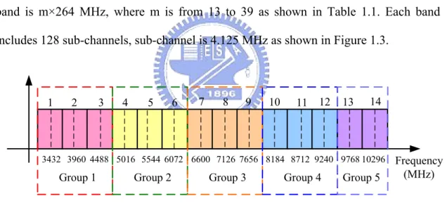
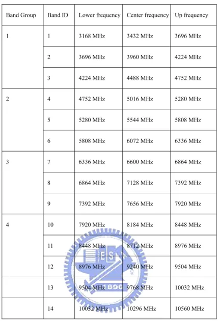
2) Multi-band orthogonal frequency division multiplexing UWB (MB-OFDM UWB) proposal [3]: In Multi-Band-OFDM (MB-OFDM) UWB, frequency span is grouped into 5 major Band Groups which are in turn sub-divided into 14 bands in total, as shown in Fig. 1.2 Each band is 528MHz bandwidth, and the center frequency of each band is m×264 MHz, where m is from 13 to 39 as shown in Table 1.1. Each band includes 128 sub-channels, sub-channel is 4.125 MHz as shown in Figure 1.3.
Frequency (MHz) 3432 3960 4488 5016 5544 6072 6600 7126 7656 8184 8712 9240 9768 10296
Group 1 Group 2 Group 3 Group 4 Group 5
1 2 3 4 5 6 7 8 9 10 11 12 13 14
Figure 1.2 Multi-band spectrum allocation
- 3 -
Band Group Band ID Lower frequency Center frequency Up frequency
1 3168 MHz 3432 MHz 3696 MHz 2 3696 MHz 3960 MHz 4224 MHz 1 3 4224 MHz 4488 MHz 4752 MHz 4 4752 MHz 5016 MHz 5280 MHz 5 5280 MHz 5544 MHz 5808 MHz 2 6 5808 MHz 6072 MHz 6336 MHz 7 6336 MHz 6600 MHz 6864 MHz 8 6864 MHz 7128 MHz 7392 MHz 3 9 7392 MHz 7656 MHz 7920 MHz 10 7920 MHz 8184 MHz 8448 MHz 11 8448 MHz 8712 MHz 8976 MHz 4 12 8976 MHz 9240 MHz 9504 MHz 13 9504 MHz 9768 MHz 10032 MHz 14 10032 MHz 10296 MHz 10560 MHz
Table 1.1 MBOA band plan
1.2 Thesis organization
This thesis discusses about the circuit design and implementation of Ultra-wideband Low-Noise amplifier and wide-band mixer, in chapter 2 and 3, respectively. In chapter 4, we will make a conclusion and discuss the future work. We will present the design flow and experimental results in TSMC 0.18-μm CMOS process. Moreover, we will discuss the reasons of differences between simulation and measurement results.
In chapter 2, this chapter includes two circuits. The first section is low-voltage ultra wide-band LNA, The second section is 3–8 GHz wideband LNA using transistor’s
- 4 -
intrinsic capacitor feedback. We will discuss these configurations, wideband input/output matching, noise and linearity of LNA. Besides, electromagnetic simulated software Sonnet and Momentum is used to approach simulated results to practical circuited property.
In Chapter 3, we will present the design and implementation of wide-band mixer for UWB applications. Firstly we review the topology and operation theory of basic mixer in section 3.1. The proposed wide-band mixer is presented in section 3.2. Section3.3 discusses layout and measurement consideration of the proposed mixer. Finally, the experiment results and comparison are presented in section 3.4.
Finally, an integrated RF receiver front-end for Ultra-wideband application is proposed in appendix. Firstly we review the architecture of receiver in section A.1. The proposed front-end circuit is presented in section A.2. Finally, the simulation results and comparison are presented in section A.3
- 5 -
Chapter 2
CMOS Low-Noise Amplifier for
UWB System
2.1 Introduction
A low-noise amplifier is the first stage, after antenna in the receiver block of a communication system. For UWB applications, the criteria to judge its performances are slightly different from narrow system. Because transmitted power spreads over a wide range and is restricted to be less than -41.3 dBm per MHz, the requirement on linearity in UWB system is not such important as in narrow system. The important requirements for UWB applications are wide-band input impedance matching, low power consumption, low noise performance, and enough gain to suppress noise of the next stages.
In order to connect to an antenna port, the first problem facing is 50 Ohm wide-band input matching. Fig. 2.1.1 shows the four basic 50 Ohm input matching techniques. However, these topologies have some drawbacks. Fig. 2.1.1 (a) is traditional source degeneration topology, because it only resonances at one frequency, it can’t achieve wide-band 50 Ohm matching. It realizes only narrow band matching. Fig. 2.1.1 (b) is the resistive termination matching, because of the loading effect, it will loss a lot of voltage if resistive termination matching is used. Fig. 2.1.1 (c) is feedback method. It can achieve wideband input matching. But because of feedback mechanism, it can’t achieve high gain to suppress noise of the next stages. Fig. 2.1.1 (d) is LC 3’rd
- 6 -
Chebyshev band-pass filter. It can perform good input matching, but it consumes large chip area because of using four inductors for input matching.
(a) (b)
(c)
(d)
Fig. 2.1.1 Conventional input matching technology
Several CMOS LNA design techniques had been reported for broadband communication applications. Recent research shows that relatively flat gain can be achieved over the 3.1- to 10.6-GHz UWB band using CMOS distributed amplifiers. However, due to the additive nature of each transistor’s gain, the distributed amplifiers
- 7 -
cannot achieve high gain. The average gain of the reported DAs is around 8 dB, which is insufficient to amplify the received UWB signal. On the other hand, as shown in Fig. 2.1.2, it requires several area consuming inductors to perform signal delay and many stages to provide a given gain that consumes much power [4-5]
Fig. 2.1.2 Conventional distributed amplifier
2.2 Ultra Wide-band Low-Noise Amplifier
2.2.1 Low-voltage, Low noise Ultra-Wideband
Amplifier
2.2.1.1 Architectures
For the UWB technology to be widely employed in the hand-held wireless applications, it cannot be avoided that power consumption is one of the main issues. So we present low-voltage UWB LNA topology.
The fundamental architecture of the low-voltage UWB LNA as shown in Fig. 2.2.1 is composed of cascode configuration and shunt peaking method. The shunt peaking method is used for the requirement of low power consumption and flat gain
- 8 -
performance over wide bandwidth [6]. The cascode structure also has good properties of better reverse isolation, frequency response, lower noise figure and less Miller effect. In order to achieve wideband input matching from 3.1 to 10.6 GHz, the three-section Chebyshev filter is used in the input matching network by combining the gate-drain parasitic capacitance of M1 and the inductance Ls.
Fig. 2.2.1 Fundamental architecture of the UWB LNA [6]
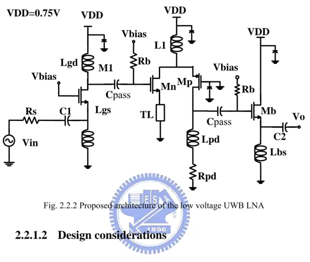
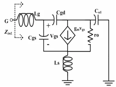
The proposed low-voltage, low-noise amplifier is shown in Fig. 2.2.2. The LNA circuit can be divided into three blocks –input matching stage, amplifying stage and output buffer stage. Here, we employ a common-gate stage and folded-cascode architecture with shunt peaking method to achieve good performance from 3.1 to 10.6G-Hz with only 0.75V supply.
For input matching stage: common-gate stage (M1) not only is suit for wideband input matching, but also can amplify RF signal. For amplifying stage: L1 is RF chock inductor which is open in small signal mode. The folded-cascode structure has good properties of better reverse isolation, frequency response, less Miller effect and low-voltage operation. Shunt peaking method (Lpd, Rpd) can enhance flat degree of power gain. TL is parasitic inductor of layout path and it can increase stability of the low-noise amplifier. An output buffer composed of common collector amplifier (Mb) is
- 9 -
added for measurement purposes.
Vin
Rs
C1
Lgs
Lgd
L1
Lpd
Lbs
Rpd
TL
VDD
VDD
VDD
Vbias
Vbias
Vbias
Cpass
Cpass
C2
VDD=0.75V
Vo
M1
Mn
Mp
Mb
Rb
Rb
Fig. 2.2.2 Proposed architecture of the low voltage UWB LNA
2.2.1.2 Design considerations
A. Input matching analysis
A common-gate (M1) is used to match to 50Ω, its small signal equivalent circuit is shown in Fig. 2.2.3. Cgs and Cgd respectively are the gate-to-source and the gate-to-drain parasitic capacitance; ro is the channel length modulation resistor of MOS
- 10 -
Fig. 2.2.3 Input small signal equivalent circuit ) ( ) ( 1 ) ( 1 1 1 w Zo r w Zo g w Zs g Z o m m in + − + + = (2-1) Where jwCgs jwLs w Zs( )= // 1 (2-2) ( ) L// 1 //Zin2 jwCgd Z w Zo = (2-3)
In equation (2-1), the third term in denominator is induced by finite channel length modulation of a MOS. To obtain more insight on the impact of ro on the input
impedance, we may assume that:
) ( ) (w jX w Zs = S (2-4) ) ( ) (w jX w Zo = o (2-5)
Equation (2-1) can be re-written by substituting (2-4) and (2-5) into (2-1) and we get
)) ( ) ( 1 ) ( 1 ( ) ) ( ) ( ( 1 ) ( ) ( 1 ) ( 1 1 2 2 2 2 2 1 w X w X r r g w X j w X r r w X g g w jX r w X jg w Xs j g Z o o o o m s o o o o m m o o o m m in ⋅ + ⋅ + + − + − ⋅ − = + − + − = (2-6) Because that 2 2( ) w X
ro + o >>gm⋅ro ⋅Xo(w)throughout the frequency of interest, the
- 11 -
Some observations can be made based on the equation (2-6): One is that the trans-conductance of the MOS transistor in common-gate configuration should be set slightly greater than 20 mS for better matching due to the effect of the MOS transistor’s finite output resistance ro, and at the resonated frequency of Ls and Cgs has the best
input reflection coefficient.
B. Noise analysis
a. Noise in MOSFETS
To develop good CMOS RF circuit design skills, a fundamental understanding of noise source in a MOSFET is necessary. In part a. section, we will focus on the inherent noise of a MOSFET, which can be categorized into two parts: drain noise source and gate noise source.
(i) Drain noise source
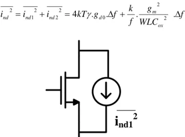
The dominant noise source in a MOSFET is the channel thermal noise, which basically is a thermal noise originated from the voltage-controlled resistor mechanism of a MOSFET. Detailed theoretically considerations lead to the following expression for the channel noise of a MOSFET, which is modeled as a shunt current noise “ 2
1
nd
i “in the output current of the device, as shown in Fig. 2.2.5. Another source of
drain noise is flicker noise. Flicker noise appears as 1/f character and is found in all active devices, as well as in some discrete passive element such as carbon resistors. In diodes, flicker noise is caused by traps associated with contamination and crystal defects in the depletion regions. In MOSFET, charge trapping phenomena are invoked in surface, and his type of noise is much greater than that of the bipolar transistor. The flicker noise in MOSFET can be given by
f A f k f WLC g f k i T ox m nd = .Δ ≈ . . .Δ 2 . 2 2 2 2 ω
- 12 -
where K is the process-dependent constant, and A is the area of the gate. Hence, the total drain noise source is given by
f WLC g f k f g kT i i i ox m d nd nd nd = + =4 . .Δ + . 2 .Δ 2 0 2 2 2 1 2 γ
i
nd12Fig. 2.2.5 channel thermal noise model
(ii) Gate noise
In addition to drain current noise, the thermal agitation of channel charge has another important consequence: gate noise. The fluctuating channel potential couples capacitively into the gate terminal, leading to a noisy gate current. Noisy gate current may also be produced by thermally noisy resistive gate material. Although this noise is negligible at low frequencies, it can dominate at radio frequencies. The gate current noise may be expressed as
f g kT ig2 =4 δ. g.Δ Where 0 2 2 . 5 d gs g g C g =ω
And δ is the coefficient of gate noise, classically equal to 4/3 for long-channel devices. The gate noise is correlated with the drain noise, with a correlation coefficient expressed as j i i i i C nd g nd g 395 . 0 2 1 2 * 1 ≈− ≡
- 13 -
The value of -0.395j is exact for long-channel devices. The correlation can be treated by expressing the gate noise as the sum of two components, the first of which is fully correlated with the drain noise, and the second of which is uncorrelated with the drain noise. Hence, the gate noise is re-expressed as
2 2 2 . 4 ) 1 ( . 4kT g c kT g c f i g g g δ δ + − = Δ
A standard MOSFET noise model can be presented in Fig. 2-2.2.6, where 2
nd
i is the
drain noise source, ig2 is the gate noise source, and
2
rg
v is thermal noise source of
gate parasitic resistor rg.
Fig. 2.2.6 MOSFET noise model
b. Common-Gate Stage Noise Analyze
Based on MOSFET noise model, the equivalent noise circuit of the proposed low-noise amplifier is shown in Fig. 2.2.7. TL is omitted because of its value is small.
- 14 -
(b)
Fig. 2.2.7 Common-gate cascade common-source stage noise circuit
The output noise PSD contributed by the source resistor is given as:
2 2 2 1 2 2 2 2 1 , | ) ( | ) 1 ( | ) ( | 4 w Z R R g w Z g g kTR S o s s m o m m s Rs n + + =
The noise contributed by the part of the induced gate noise in M1 that is fully
uncorrelated with the drain noise is given by:
Rs n m s gs s s s m o m m s gs u g n S g R C w c w Z R R g w Z g g R C w c kT S , 1 2 1 2 2 2 2 2 1 2 2 2 1 2 2 1 2 2 1 , , , 5 ) | | 1 ( ] | ) ( | ) 1 [( 5 | ) ( | ) | | 1 ( 4 ⋅ ⋅ − ⋅ = + + ⋅ ⋅ − ⋅ = αδ αδ
The output noise PSD due to the two noise sources in M1 is then given by:
Rs n s m s gs m gs s s s s m c d g n S w Z jg R wC c g c w C R w Z R R g S , 1 1 2 1 2 2 2 1 2 2 1 1 , , , , ] ) ( 5 | | 2 5 | | ) | ) ( | 1 ( [ + + + ⋅ ⋅ = γδ αδ α γ
Where the first term is contributed by the channel thermal noise of M1, the second term
by the correlated part of the induced gate noise, and the last term arises from the correlation of these two noise sources. The noise contributions by M2 are given by:
Rs n s m s s m s m gs u g n S w Z g R R g R g c w C S 2 2 , 1 2 2 1 2 2 2 2 1 2 , , , ]} | ) ( | ) 1 [( 5 ) | | 1 ( { ⋅ ⋅ + + ⋅ ⋅ − = αδ
- 15 - Rs n s m S S m T S T S m S gs m s gs m c d g n S w Z g R R g w Z jR w c Z R w c w Z g R C w c Z g kT j w Z C w c kT g kT S , 2 1 2 2 2 1 2 0 2 0 2 2 2 2 2 0 2 2 0 2 2 2 2 2 2 2 2 , , , , | ) ( | ) 1 ( | ) ( | 5 | | 2 5 | | | ) ( | 5 | | 8 | ) ( | | | 5 4 4 ⋅ ⎥ ⎦ ⎤ ⎢ ⎣ ⎡ ⋅ + + ⋅ ⎟ ⎟ ⎟ ⎟ ⎠ ⎞ ⎜ ⎜ ⎜ ⎜ ⎝ ⎛ ⋅ ⋅ ⋅ ⋅ + ⋅ ⋅ ⋅ + ⋅ = ⋅ ⋅ ⋅ ⋅ ⋅ ⋅ − ⋅ ⋅ ⋅ ⋅ + = ω γδ ω δ α α γ γδ αδ α γ
The total noise factor is derived as:
Rs n c d g n Rs n u g n Rs n c d g n u g n c d g n u g n
S
S
S
S
F
S
S
S
S
S
F
, 2 , , , , , 2 , , , 1 , 2 , , , , 2 , , , 1 , , , , 1 , , ,1
+
+
+
+
=
+
+
=
F1 is the noise factor of the single common-gate stage, excluding the effect of the noise
contributed by the common source stage which is given by the later two terms. Where F1 is given by:
) ( 5 | | 2 5 | | ) | ) ( | 1 ( 5 ) | | 1 ( 1 1 1 1 2 1 2 2 2 2 1 1 1 2 2 1 w Zs jg R wC c g R C w c w Zs R g R g Rs Cgs w C F m s gs m s gs s m s m δγ αδ α γ αδ + + + + − + = (2-7) Where jwCgs jwLs w Zs( )= // 1
In equation (2-7), because gm1 is in the denominator, the trans-conductance (gm1) of M1
should be increased to decrease noise factor and at the resonated frequency of Ls and Cgs has the minimal noise figure. But the input matching will be worse than -10dB when gm1 increases to 35 mS. There is a trade-off between input matching and noise
factor for common-gate circuit. For the proposed circuit , gm1 is set about 33ms to
decrease noise factor, but input return loss still better than -10db.
C. Gain analysis (Shunt peaking method)
Shunt peaking is a bandwidth extension technique in which an inductor connected in series with the load resistor shunts the output capacitor C. A common-source amplifier with shunt peaking is shown in Fig. 2.2.8. For the shunt-peaked network:
- 16 -
The inductor introduces a zero in Z(s) that increases the impedance with frequency, compensates the decreasing impedance of C, and thus extends the -3 dB bandwidth. The magnitude of the impedance, normalized to the DC value as a function of frequency, is then
so that
where ω1 is the uncompensated -3dB frequency. We can choose congruous m to
achieve flat wide-band gain.
Fig. 2.2.8 A common-source amplifier with bridged-shunt peaking.
2.2.2 3–8 GHz wideband LNA Using Capacitor
Feedback
2.2.2.1 Architectures
A simple wide-band input matching network is present in a standard 0.18um CMOS technology in this section. The proposed circuit using transistor’s intrinsic capacitor
- 17 -
feedback achieve -10 dB input reflection coefficient from 2.75 GHz to 12 GHz. Compared with traditional matching network of narrow band LNA, such matching mechanism is not an additional inductor, input broadband matching still can be reached. The fabricated wideband LNA achieves average power gain (S21) of about 10 dB from 2.75-GHz to 7.7-GHz .From the bandwidth, the broadband LNA exhibits a noise figure of 3.64–5.5 dB. The DC supply is 1.5 V.
Fig. 2.2.9 Topology of the proposed UWB LNA
Fig. 2.2.9 shows the schematic of the proposed wideband LNA circuit composed of common source stage and common gate stage. L1 and L2 are RF choke inductors which are open in small signal mode. M1、M2、Rd、Ld form cascode amplifier with shunt-peaking load to achieve flat power gain, better reverse isolation, better frequency response, lower noise figure and less Miller effect. An output buffer composed of common collector amplifier is added for measurement purposes.
2.2.2.2 Design considerations
A. Input matching analysis [30]
- 18 -
the small signal circuit of the proposed wide-band LNA. In order to analyze the input-matching network, the small signal circuit of the wideband LNA is decomposed into two parts. One is resistor feedback in high frequency mode, the other one is capacitor feedback in low frequency mode, as shown in Fig. 2.2.11 (a) (b), respectively.
Fig.2.2.10 LNA small signal diagram
- 19 -
Fig. 2.2.11 (b) LNA small signal diagram in low frequency mode
At high frequency mode small signal circuit as shown in Fig. 2.2.11 (a): Using KCL KVL theory, approximate input impedance can be got that:
(1)
Where
s i o oL
j
R
r
r
ω
φ
+
+
=
2 it is assumed that jωLS << jωCgsFig. 2.2.11 (C) Low frequency mode input port equivalent circuit
At low frequency mode as shown in Fig. 2.2.11 (b): Using KCL KVL theory, approximate input impedance equivalent circuit can be shown in Fig. 2.2.11. (c). Because Cβ Lβ are much small and Rβ is much large, B2 branch is omitted. B1 branch
1 2)] 1 ( 1 )[ 1 ( + ⋅ ⋅ + + ⋅ ⋅ − ⋅ + = m i g gd g m s g g inH g R C C C g L C j L j Z φ φ ω ω
- 20 -
dominates the low frequency mode impedance function. Where:
gd m O C g C Rρ = 1 ,
C
ρ=
g
mr
oC
gd , 1 (1 m o) gd o m o s g r C r g C L Lρ = +The matching frequency at low frequency mode is that:
)
1
(
)
(
2
1
)
(
2
1
1 mo o s g gd o m g Lowr
g
C
L
L
C
r
g
L
L
C
f
+
+
=
+
=
π
π
ρ ρ (2)To make use of equation of (1) and (2), two-frequency matching mechanism is realized and wideband input matching can be achieved.
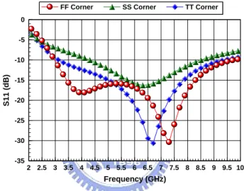
2 2.5 3 3.5 4 4.5 5 5.5 6 6.5 7 7.5 8 8.5 9 9.5 10 Frequency (GHz) -35 -30 -25 -20 -15 -10 -5 0 S 1 1 ( d B )
FF Corner SS Corner TT Corner
Fig. 2.2.12 S11 of the proposed LNA
2.3 Chip implementation and measured result
A. Measurement consideration
The two UWB Low-Noise amplifiers are designed for on-wafer testing. Therefore the arrangement of each pad must satisfy rules of CIC’s (Chip Implementation Center’s) probe station testing rules.
For folded LNA: Two six-pin dc probes are required to feed with dc voltages. In addition, two RF probes are also needed for RF signals.
- 21 -
Fig. 2.3.1 (a) On-wafer measurement of low-voltage UWB LNA test diagram
For 3-8 GHz capacitor feedback LNA: One six-pin dc probe, one three-pin dc probe and two RF probes are required. Fig 2.2.13 (a~c) shows the arrangement for dc and RF probes.
Fig. 2.3.1 (b) On-wafer measurement of 3-8 GHz LNA test diagram
- 22 -
The measurement equipments include a network analyzer ( HP8510C ), a noise analyzer ( Agilent N8975A ), a spectrum analyzer ( Agilent E4407B ), two signal generators, and several dc power supplies. The measurement setups for S-parameter, noise figure are shown in Fig. 2.2.14 (a~b). We use the RF IC measurement system powered by LabView to measure the linearity of the UWB LNA. The measurement setups for 1-dB compression point (P1dB), IIP3 are shown in Fig. 2.2.14 (c~d). We will discuss the experimental and testing resultsof this circuit in following sections.
HP-8510C network analyzer N 8975A 之雜訊分析儀
- 23 -
(c)
(d)
Fig. 2.3.2 Measurement setups for (a) S-parameter (b) noise figure (c) P1dB (d) IIP3
B. Folded UWB LNA Measurement result
The layout and chip photo of the proposed folded UWB LNA is shown in Fig 2.2.15 and Fig 2.2.16, respectively. A DC block capacitor is needed in the input of the UWB LNA to isolate the dc between circuit and equipment.
- 24 -
Fig 2.3.3 Layout of the proposed low-voltage LNA
Fig2.3.4 Micrograph of the proposed low-voltage LNA
This work is designed and processed using TSMC 0.18µm mixed-signal/RF CMOS 1P6M technology. The S-parameter are shown in Fig. 2.2.17(a) (b), Fig. 2.2.18 and Fig. 2.2.19, where the measured S11 < -10dB and S22 < -9 dB from 3.1 GHz to 10.6 GHz, except the point which produces peak value. The power gain (S21) is around 7.5dB from 3.1 to 7.5 GHz, the 3dB bandwidth is 2.9-8.7 GHz. The measured noise figure of
- 25 -
4.8-7.5 dB from 2.75 to 7.7 GHz has been presented in the proposed as shown in Fig. 2.2.20. The measured P1dB are -14dBm at 5.1 GHz, and -10dBm at 7.5 GHz in Fig.
2.2.21. The measured IIP3 are -4dBm at 5.1 GHz, and -1.2dBm at 7.5 GHz in Fig. 2.2.22.Table2.2.1 summarizes the measured data of proposed wideband LNA.
2 2.5 3 3.5 4 4.5 5 5.5 6 6.5 7 7.5 8 8.5 9 9.5 10 10.5 11 Frequency (GHz) -28 -24 -20 -16 -12 -8 -4 0 4 8 12 16 20 Measurement S21 Simulation S21
- 26 - 2 2.5 3 3.5 4 4.5 5 5.5 6 6.5 7 7.5 8 8.5 9 9.5 10 10.5 11 Frequency (GHz) -90 -80 -70 -60 -50 -40 -30 Measurement S12 Simulation S12
Fig. 2.3.5 (b) Isolation vs. Frequency
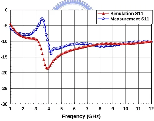
1 2 3 4 5 6 7 8 9 10 11 12 Freqency (GHz) -30 -25 -20 -15 -10 -5 0 Simulation S11 Measurement S11
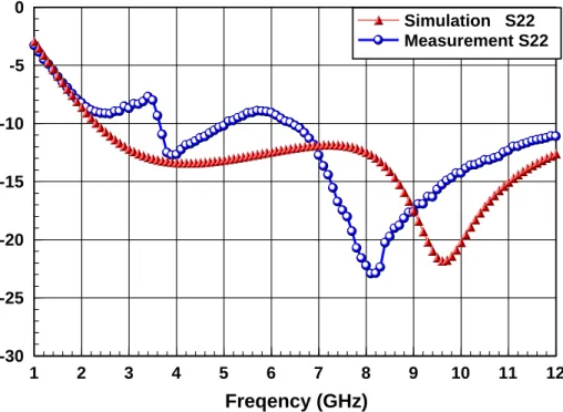
- 27 - 1 2 3 4 5 6 7 8 9 10 11 12 Freqency (GHz) -30 -25 -20 -15 -10 -5 0 Simulation S22 Measurement S22
Fig. 2.3.7 Output return loss coefficient vs. Frequency
3 4 5 6 7 8 9 10 11 12 Freqency (GHz) 1 2 3 4 5 6 7 8 9 10 N F ( d B ) Simulation NF Measument NF
- 28 - -30 -25 -20 -15 -10 -5 0 Power RF (dBm) -4 -3 -2 -1 0 1 2 3 4 5 6 7 8 9 10 11 12 Simulation Measurement Fig. 2.3.9 (a) P1db at 5.1 GHz -30 -25 -20 -15 -10 -5 0 Power RF (dBm) -4 -3 -2 -1 0 1 2 3 4 5 6 7 8 9 10 11 12 13 14 Simulation Measurement Fig. 2.3.9 (b) P1db at 7.5 GHz
- 29 - -40 -35 -30 -25 -20 -15 -10 -5 0 Power RF (dBm) -100 -90 -80 -70 -60 -50 -40 -30 -20 -10 0 Measurement Simulation
Fig. 2.3.10 (a) IIP3 at 5.1 GHz
-40 -35 -30 -25 -20 -15 -10 -5 0 Power RF (dBm) -100 -90 -80 -70 -60 -50 -40 -30 -20 -10 0 Measurement Simulation Fig. 2.3.10 (b) IIP3 at 7.5 GHz
- 30 -
Table.2.3.1 Performance summary of the proposed LNA
Specification Measurement Post Simulation
BW (GHz) 3 - 7.5 3 - 10
S11 (dB) <-10 <-10
S22 (dB) <-9 <-10
S21 (dB) 7.5 (flat gain) 10.5 (flat gain)
S12 (dB) <-34 <-50 Noise Figure (dB) 4.8-7.5 3.1-5.1 P1dB (dBm) -14 * -16 * IIP3 (dBm) -4 * -6.5 * Vdd (V) 0.75 V 0.75 V Total Power (mW) 11 11.3 *at 5.1 GHz
C. Capacitor Feedback UWB LNA Measurement result
The layout and microphotograph of the UWB LNA circuit is shown in Fig. 2.3.11 and 12, respectively. The circuit is fabricated in the TSMC 0.18μm CMOS process technology. The die area including bonding pads is 0.825 mm by 0.94 mm.
- 31 -
Fig. 2.3.12 (b) Photograph of UWB LNA (0.88*0.93mm2)
The S-parameter of simulation and measured results are plotted as shown from Fig.2.2.24 to Fig.2.2.26. The measured power gain S21 achieves the maximum value of 10.8dB at 2.7 GHz and the 3-dB bandwidth of power gain is from 1.9 GHz to 8.2 GHz. The variation of inductor (Ld) lead to shunt peaking method don’t achieve adaptable m to enhance bandwidth and thus the power gain in high frequency will become small. The average simulated and measured result of S22 are both smaller than -10dB, as shown in Fig.2.2.26.The S11 is shown in Fig .2.2.25. The measured result shows that the proposed circuit using transistor’s intrinsic capacitor feedback achieve -10 dB input reflection coefficient from 2.75 GHz to 12 GHz. The measurement and simulation result of noise, NF, is shown in Fig.2.2.27. The simulated minimum noise figure is 2.45dB at 5GHz, and the average noise figure is about 2.6dB. The measured minimum noise figure is 3.64dB at 3 GHz, and the average noise figure is about 4.6dB. Fig.2.2.28. is the simulation and measurement result of the input 1 dB compression point (P1dB). The two-tone test measured results for third-order intermodulation distortion are shown in Fig. 2.2.29. The measured result of IIP3 is -1.8 dBm and 1 dBm at 4.1 GHz and 7.5 GHz, individually. The core current of the proposed LNA is 15mA with a power supply
- 32 -
1.5V. Table 2.2.2 is the summary of simulated and measured performance of the proposed amplifier. 1.5 2 2.5 3 3.5 4 4.5 5 5.5 6 6.5 7 7.5 8 8.5 9 9.5 10 Frequency (GHz) 0 1 2 3 4 5 6 7 8 9 10 11 12 13 14 S2 1 (d B ) Simulation S21 Measurement S21
Fig. 2.3.13 S parameter vs. frequency
2 3 4 5 6 7 8 9 10 11 12 13 Freqency (GHz) -40 -35 -30 -25 -20 -15 -10 -5 0 S 1 1 ( d B ) Measument S11 Simulation S11 Fig. 2.3.14 S11 vs. frequency
- 33 - 1 1.5 2 2.5 3 3.5 4 4.5 5 5.5 6 6.5 7 7.5 8 8.5 9 9.5 10 Frequency (GHz) -50 -45 -40 -35 -30 -25 -20 -15 -10 -5 0 Simulation S12 Measurement S12 Simulation S22 Measurement S22 Fig. 2.3.15 S22 vs. frequency 1.5 2 2.5 3 3.5 4 4.5 5 5.5 6 6.5 7 7.5 8 8.5 9 Frequency (GHz) 2 3 4 5 6 7 N F (dB )
- 34 - 3 3.5 4 4.5 5 5.5 6 6.5 7 7.5 8 Freqency (GHz) -20 -18 -16 -14 -12 -10 -8 -6 -4 -2 0 P o w e r R F ( d B m ) Simulation Measument
Fig. 2.3.17 Input 1 dB compression point vs. frequency
-40 -36 -32 -28 -24 -20 -16 -12 -8 -4 0 4 8 Power RF (dBm) -100 -80 -60 -40 -20 0 Measurement Simulation
- 35 - -40 -36 -32 -28 -24 -20 -16 -12 -8 -4 0 4 8 Power RF (dBm) -100 -80 -60 -40 -20 0 Measurement Simulation Fig. 2.3.18 (b) at 7.5 GHz
Table.2.3.2 Performance summary of the proposed LNA
Simulation
Measurement
VDD 1.5 1.5
Band Width
3.1Ghz-8.1Ghz
2.75-7.7Ghz
3dB-bandwidth 1.9-9.5Ghz 1.8-8.3Ghz
S21
max(dB) 12.8 10.8
S11(dB)
< -10.1
< -10.0
S22(dB)
< -12
< -10
NF
average(dB) 2.6 4.6
P1db(dBm) >-13 >-14
IIP3(dBm) at 4 GHz
-3
-1.8
UWB LNA Current
15mA
15.3mA
- 36 -
2.4 Comparison and Discussion
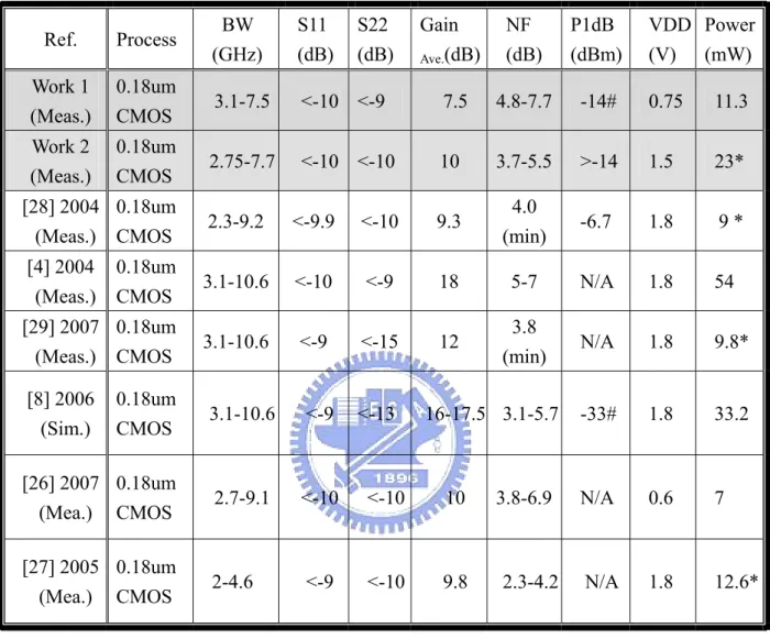
Table 2.4.1 Comparison of Ultra Wide-band LNA Ref. Process BW (GHz) S11 (dB) S22 (dB) Gain Ave.(dB) NF (dB) P1dB (dBm) VDD (V) Power (mW) Work 1 (Meas.) 0.18um CMOS 3.1-7.5 <-10 <-9 7.5 4.8-7.7 -14# 0.75 11.3 Work 2 (Meas.) 0.18um CMOS 2.75-7.7 <-10 <-10 10 3.7-5.5 >-14 1.5 23* [28] 2004 (Meas.) 0.18um CMOS 2.3-9.2 <-9.9 <-10 9.3 4.0 (min) -6.7 1.8 9 * [4] 2004 (Meas.) 0.18um CMOS 3.1-10.6 <-10 <-9 18 5-7 N/A 1.8 54 [29] 2007 (Meas.) 0.18um CMOS 3.1-10.6 <-9 <-15 12 3.8 (min) N/A 1.8 9.8* [8] 2006 (Sim.) 0.18um CMOS 3.1-10.6 <-9 <-13 16-17.5 3.1-5.7 -33# 1.8 33.2 [26] 2007 (Mea.) 0.18um CMOS 2.7-9.1 <-10 <-10 10 3.8-6.9 N/A 0.6 7 [27] 2005 (Mea.) 0.18um CMOS 2-4.6 <-9 <-10 9.8 2.3-4.2 N/A 1.8 12.6* # at 5 GHz *Core circuit
In the first work (Low-voltage UWB LNA) which reveal wideband performance under low voltage situation. But it is unexpected in the measured results at 3-4 GHz as simulation. Because the fabricated inductor value of TL (common source degeneration inductor) is not expected as simulated inductor value of TL, it causes the circuit is seemly unstable at 3-4 GHz. The unstable behaviors make the S11 and S22 to produce peaking value as measured results. And the variation of inductor (Ld) lead to shunt peaking method don’t achieve adaptable m to enhance bandwidth and thus the power
- 37 -
gain in high frequency will become small. The phenomenon of decreasing power gain in high frequency is maybe caused by parasitic capacitor of layout path. The second work (3-8 GHz capacitor feedback wideband low noise amplifier) which achieves perfect ultra wide-band input impedance matching from 2.75 to 12 GHz. The measured noise figure is greater than simulated result about 2 dB, it may be caused by the inexactitude noise model and the abridgement of power gain. Table 2.4.1 shows the comparisons of these two works and other recently ultra wide-band LNA papers.
- 38 -
Chapter 3 A Folded Current-Reused
Mixer for
UWB Applications
System
3.1 Introduction
Fig. 3.1.1 shows the architecture of UWB receiver. The mixer of the receiver is introduced in this chapter. In order to realize ultra wide-band circuits, many specialized technologies and devices like SiGe, GaAs, InP, HBT and HEMT have been employed. Although using specialized technologies and devices can achieve good performances, but there are some drawbacks such as high dc power consumption, high supply voltage and were not suitable for UWB system applications.
Fig. 3.1.1 Block diagram of a UWB receiver [7]
A distributed mixer has been designed in 0.18um CMOS technology [9], as shown in Fig 3.1.2. Although the design exhibits good noise performance, but the bandwidth could not cover the entire frequency band from 3.1 to 10.6 GHz and large die area is needed.
- 39 -
Fig 3.1.2 Ultra wide-Band Distributed CMOS Mixer [9]
A CMOS UWB mixer has been designed in 2004 year as shown in Fig 3.1.3 [10]. This design has some disadvantages. It uses multiple voltage sources, the values of which are 3.3-5V. And its power consumption is high.
Fig 3.1.3 CMOS Ultra wide-Band Mixer [10]
In this work, a wide-band mixer based on Gilbert cell architecture combined with folded current-reused pair is proposed in 0.18μm CMOS technology. It still achieves high conversion power gain in low dc power consumption and low supply voltage
- 40 -
situation. The proposed mixer achieves a simulated conversion power gain of 10.3-13.7 dB and double side-band noise figure of 11.1-14.7 dB from 3.1 to 10.6 GHz with a fixed IF of 100 MHz under dc power consumption of 10.95 mW.
3.2 Review of basic mixer
3.2.1
Basic mixer topology
The mixer is a frequency translation device. The operation function of the mixer can be shown in Fig 3.2.1. It performs frequency translations by multiplication of a RF signal and a LO signal.
]
)
cos(
)
[cos(
2
)
cos
(
)
cos
(
A
ω
1t
•
B
ω
2t
=
AB
ω
1−
ω
2t
+
ω
1+
ω
2t
Fig 3.2.1 Operation of mixer
Based on the mixer topologies, the mixer can be divided into three parts: Single balance mixer, double balance mixer, passive mixer [11] [12] [13] [14].
A. Single balance mixer
Fig 3.2.2 shows a single balance mixer which is a switching type mixer. Feed-through is a basic problem in switching mixer. But the problem can be eliminated by using a differential IF output and polarity reversing LO switch called “Single balance mixer”. It consists of three stages. One is the trans-conductance stage which
- 41 -
converts the RF voltage in a current. One is the switching stage which performs multiplication to RF current into IF current. One is the load stage which converts IF current into IF voltage. The LO function is shown in equations (3-1).
Switching Function [11] ...] t) sin(3 3 1 t) [sin( 4 (t) T (t) T Wave Square T(t)= = 1 + 2 = ωLo + ωLo + π (3-1) So ...} ] ) sin( ) [sin( 2 1 ) sin( { 4 ...] ) 3 sin( 3 1 ) [sin( 4 ] ) cos( [ ) ( + − + + + = + + ⋅ + ⋅ = t w w t w w v g t w I R t w t w t w v g I R t V LO RF LO RF RF m LO DC L LO LO RF RF m DC L IF π π (3-2) Conversion Gain=
π
m LR
g
2
- 42 -
B. Double balance mixer
Single balance mixer still has LO feed-through problem. Fig 3.2.3 shows a double balance mixer which can eliminate the drawback of LO feed-through.
For double balance mixer:
...] ) 3 sin( 3 1 ] )[sin( cos( 8 ...] ) 3 sin( 3 1 ] [sin( 4 )] cos( [ ...] ) 3 sin( 3 1 ) [sin( 4 )] cos( [ ) ( + + = + + ⋅ − − + + ⋅ + = t t t v g R t t t v g I R t t t v g I R t V LO LO RF RF m L LO LO RF RF m DC L LO LO RF RF m DC L IF ω ω ω π ω ω π ω ω ω π ω (3-3)
Double balance mixer removes the LO feed-through because the DC term cancels.
- 43 -
3.2.2 Some special mixer topology
A. Conversion Gain Enhancement
Fig 3.2.4 Negative resistor Load Gilbert Cell Mixer [15]
Fig 3.2.5 Negative resistor topology [16]
- 44 -
topology is shown in Fig 3.2.5. Conversion gain equation can be driven as shown:
load m
R
g
CG
2
.
.
π
=
(3-4) , where m load loadg
R
Z
=
//
−
2
We can tune the bias voltage befittingly to get the optimum conversion gain and linearly. The transistors of M4 and M5 can increase isolation between LO port and RF port.
B. Current Bleeding Method [17]
From equation (3-3), the mixer gain for a CMOS double balance type mixer is given by
π
π
2 2 L SS n L m v g R K I R A = = (3-5) And the IP3 of the CMOS Gilbert mixer is approximately given asn K Iss IP = ⋅ 3 32 3
The mixer gain and IIP3 is therefore proportional to . Consequently, it seems that an arbitrary increase in the bias current can improve the conversion gain and IP3. But consider the consequence of increasing the bias current, Ohm’s Law dictates that the voltage dropped across RL increases and the head-room voltage decreases. The output signal will therefore eventually compress at a lower level of signal input. IP3 is then lower, and the overall performance of the mixer is degraded. A method called charge injection as shown Fig 3.2.6 in can achieve conversion gain and linearity at the same time.
- 45 -
Fig 3.2.6 A Gilbert Cell mixer with charge injection
An additional current source can draw out the current which flows through load stage, so it can enhance the head-room voltage. And a single current source can decrease noise of the mixer.
C. LINEARIZATION TECHNIQUE FOR GILBERT CELL
MIXER
- 46 -
Figure 3.2.7 is a compensative circuit for linearization. The IIP3 of the mixer is approximately given as:
Ba RFa RFa B RF RF Ba RFa B RF I K K I K K I K I K IIP − − ⋅ = 3 32 3 (3-6)
In equation (3-6), we let denominator to be zero. We can cancel the third-order distortion term effectively. In other word, we should let
) ( RF RFa B Ba K K I I =
In this case, ideally we can obtain a very high intercept point (IIP3 →∞). But there
are many limiting factors in achieving a very high IIP3 for multiple differential pair mixer in reality: mismatches, the simplified models and the parasitic effects.
3.3 Folded current-reused Ultra-band mixer
Fig. 3.3.1 Topology of the proposed UWB mixer
Fig. 3.3.1 shows the schematic of the proposed wide-band folded current-reused mixer circuit. The mixer circuit can be divided into five blocks- RF matching network,
- 47 -
RF trans-conductance stage, LO switching stage, active load and IF common collector amplifier.
For RF matching network is shown in Fig. 3.3.2, the second order LC ladder filter which can be equivalent to chebyshev filter is used to achieve wide-band frequency response from 3.1 GHz to 10.6 GHz. The behavior of this circuit is sensitive to the pad capacitance. If the pad capacitance increases, the return loss curve is degraded. The pad size is reduced to 50*50um2 .The parasitic capacitor of pad is only 30~35 fF.
Fig. 3.3.2 RF matching network
For LO port, there is no matching circuit, because of the switch stage biasing in the edge of subthreshold region and saturation region. The transistors M9 and M10 form the simple active load with common mode feedback circuit. It can stabilize the drain voltage of the switched transistors (M5, M6, M7, and M8). In contrast to the conventional Gilbert cell mixer, the proposed mixer replaces the traditional common source trans-conductance stage with a folded current-reused pair. It not only reduces the supply voltage, but also increases trans-conductance (gm) effectively. Such folded
current-reused structure can uses DC current effectively because that the main current flows through trans-conductance stage, switching stage only consumes 100uA. The maximum conversion gain of the folded current-reuse mixer can also be verified as following:
- 48 - ...] ) 3 sin( 3 1 ] )[sin( cos( ) ( 8 ...] ) 3 sin( 3 1 ] [sin( 4 )] cos( ) ( [ ...] ) 3 sin( 3 1 ] [sin( 4 )] cos( ) ( [ ) ( + + + = + + ⋅ + − − + + ⋅ + + = t t t v g g R t t t v g g I R t t t v g g I R t V LO LO RF RF mp mn L LO LO RF RF mp mn DC L LO LO RF RF mp mn DC L IF ω ω ω π ω ω π ω ω ω π ω
)
(
2
mp mn Lg
g
R
Gain
Conversion
=
+
π
WhereR
L=
R
LOAD//
r
oWhen RLOAD is increased to provide conversion gain, the CMFB circuit can prevent
the dropping of the drain voltage of the switched transistors. This will provide a good linearity when the conversion gain is increased. An output buffer composed of common collector amplifier is added for measurement purposes.
3.4
Chip implementation and measured considerations
Fig. 3.4.1 is the layout of the proposed Ultra wideband mixer. In order to decrease the degree of mismatches, we focus on the symmetry of layout very much. The layout seems to be perfect symmetric except for the different layer of metal. Fig. 3.4.2 is the die photograph of the proposed Ultra wideband mixer.- 49 -
Fig. 3.4.2 Die photograph of the proposed ultra wide-band mixer
The Ultra wideband mixer is designed for on-wafer measurement so the layout must follow the rules of CIC’s (Chip Implementation Center’s) probe station testing rules. Fig. 3.4.3 shows the on-wafer measurement setup with four probes.
Fig.3.4.3 On wafer measurement for UWB Mixer
The simplified measurement setups are shown in Fig. 3.4.4 (a~d). We use the RF IC measurement system powered by LabView to measure the linearity and conversion power gain of the UWB mixer. The whole measurement environment in CIC is shown in Fig. 3.4.5.
- 50 - Network Analyzer . Signal Generator Spectrum Analyzer
Balun
Signal GeneratorBalun
Balun
RF Port LO Port (a) (b) Signal Generator1 Spectrum AnalyzerBalun
Signal GeneratorBalun
Balun
RF Port LO Port Signal Generator2 Combiner (c)- 51 - Signal Generator
Balun
LO Port CAL Plane CAL Plane Noise Figure AnalyzerBalun
Balun
Noi se So urce (d)Fig. 3.4.4 Measurement setup of the proposed switched Gm sub-harmonic mixer for (a) input return loss (b) conversion gain and P1dB (c) IIP3 (d) noise figure
- 52 -
3.5 Measurement results and discussion
3.5.1
Measurement results
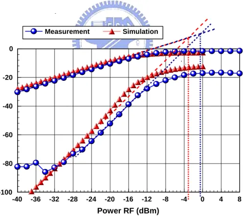
In this section, the measured results are shown below. This folded current-reused mixer consumes 7.5mA and the buffer consumes 7.1mA dc current with 1.5 V power supply. As shown in Fig. 3.5.1, the measured RF port input return loss are better than -10dB through 3.1-8 GHz. As shown in Fig. 3.5.2, the measured IF port input return loss are better than -10dB through 100-528 MHz. Fig. 3.5.3 (A) ~ (M) shows the conversion power gain with lo power sweeping. It reveals that a high conversion power gain is achieved in this work. In simulation, the conversion power gain has maximum, when Lo power is during -4 and -1 dBm, but in measurement, the conversion power gain has maximum, when Lo power is during -12 and -8 dBm. Fig 3.5.4 shows that the measured results reveal that conversion power gain are 13.5-15.5 dB from 3.1 to 8 GHz. Fig. 3.5.5 shows the DSB noise figure with the IF=150 MHz. It reveals that the DSB noise figure is 11-14.5 during 3.1-8 GHz. Fig. 3.5.6 shows that the P1dB of the proposed mixer is about -24dBm to -26 dBm. Fig. 3.5.7 shows the input 3rd order intercept point (IIP3) of -11.5 dBm at 6072 MHz. Finally, Fig. 3.5.8 shows the isolation with frequency between RF and LO port.
- 53 - 0 1 2 3 4 5 6 7 8 9 10 11 12 Frequency (GHz) -30 -25 -20 -15 -10 -5 0 R F R e tu rn L o s s ( d B ) Simulation Measurement
Fig. 3.5.1 RF port input return loss
100 200 300 400 500 600 700 800 900 1000 Frequency (MHz) -20 -19 -18 -17 -16 -15 -14 -13 -12 -11 -10 IF S parameter
Fig. 3.5.2 IF port input return loss
-16 -15 -14 -13 -12 -11 -10 -9 -8 -7 -6 -5 -4 -3 -2 -1 0 LO Power (dBm) 0 1 2 3 4 5 6 7 8 9 10 11 12 13 14 15 16 17 18 19 20 C o n v e rs io n G a in ( d B ) Measurement Simulation -19 -18 -17 -16 -15 -14 -13 -12 -11 -10 -9 -8 -7 -6 -5 -4 -3 -2 -1 0 LO Power (dBm) 0 1 2 3 4 5 6 7 8 9 10 11 12 13 14 15 16 17 18 19 20 C o n v e rs io n G a in ( d B ) Measurement Simulation