The Characteristics and Control of Body-to-Body Leakage
Current in PD-SOI
H. C. Lo,a,b,zW. C. Luo,cW. Y. Lu,aC. F. Cheng,a T. L. Chen,aC. H. Lien,b S. K. H. Fung,aand C. C. Wua
a
Taiwan Semiconductor Manufacturing Company Limited, Hsinchu 30078, Taiwan
b
Institute of Electronics Engineering, National Tsing Hua University, Hsinchu 30013, Taiwan
c
Institute of Electronics Engineering, National Chiao Tung University, Hsinchu 30010, Taiwan
Body-to-body leakage共BBL兲 current in a partially depleted silicon-on-insulator 共PD-SOI兲 device is increased significantly as polyspacing共PS兲 is reduced in technology scaling. We found out that the BBL has a great impact to Vt variation. We have demonstrated that the BBL can be minimized drastically by implant optimization. The dependence of the BBL on silicon film thickness, e-SiGe structure, and dopant diffusivity is also discussed in this paper. The layout effect of the BBL current in PD-SOI devices has been characterized with different PSs, device widths, and polylengths. Finally, we have demonstrated that the BBL current can be reduced below junction leakage level.
© 2009 The Electrochemical Society. 关DOI: 10.1149/1.3223971兴 All rights reserved.
Manuscript submitted June 16, 2009; revised manuscript received August 17, 2009. Published September 25, 2009.
Silicon-on-insulator共SOI兲 complementary metal oxide semicon-ductor共CMOS兲 has been widely used recently due to its better de-vice performance and scalability. Partially depleted silicon-on-insulator共PD-SOI兲 has a similar device structure to a bulk device. As a consequence, the PD-SOI can be fabricated in a standard bulk CMOS process. SOI devices have better circuit performance and lower power consumption due to lower channel doping and smaller parasitic capacitances. However, PD-SOI devices possess several unique behaviors that do not exist in bulk devices such as kink effect,1-3self-heating effect,4-6history delay effect,7,8and pass-gate leakage.9,10Those effects have been actively studied and modeled. For the two stack PD-SOI devices sharing a common diffusion area, the bodies of the two devices are isolated by a common source/drain 共S/D兲 junction. If the common S/D junction does not abut the buried oxide共BOX兲, a leakage path is formed between the two bodies. The body-to-body leakage共BBL兲 induces body potential change and Vt shift, as reported in Refs.11 and 12. Besides, ac performance is degraded because of the increase in the S/D junction capacitance. In an advanced SOI technology, aggressive scaling of the junction depth leads to a significant increase in the BBL current. The BBL can have the following adverse effects on circuit operation: 共i兲 Higher junction capacitance due to the larger junction area,共ii兲 Vt shift due to the change in body potential, and共iii兲 failure of circuit function if device Vt is significantly changed. As a result, the BBL effect must be taken into consideration when optimizing the S/D junction profile in PD-SOI devices.
The accuracy of device modeling becomes increasingly impor-tant in modern circuit design. Although several attempts have been made on the modeling and simulation of the BBL, very few experi-mental results have been reported. The BBL effect also depends on the device geometries such as polygate spacing. The geometry effect must also be taken into consideration when optimizing the S/D junc-tion profile.
This paper presents the experimental and simulation results of the BBL effect and its dependences on back-gate bias, polygate spacing, device width, silicon layer thickness, and S/D implant con-ditions. The impact of the Vb shift to circuit function caused by the BBL in stack PD-SOI devices has been simulated by using a simu-lation program with integrated circuit emphasis 共SPICE兲 circuit simulator. Finally, experimental results are presented to demonstrate that the BBL current can be reduced to below junction leakage cur-rent by process optimization and device geometry techniques.
Device Fabrication and Measurement
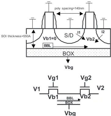
The PD-SOI metal-oxide-semiconductor field-effect transistors 共MOSFETs兲 used in this study were fabricated in a 45 nm SOI
process. This process utilizes several advanced strained techniques to boost device performance like its counterpart bulk process, in-cluding embedded SiGe 共e-SiGe兲,13,14 dual contact-etch-stop-layer,15,16and stress memorization technique.17-20The structure used to characterize the BBL effect is composed of two stack body-tie devices sharing a common well. The measurement setup is shown in Fig.1. Body bias共Vb2兲 is applied to the body region b2. The BBL current is the body current of device no. 1, in which the S/D-to-body junction bias is zero to exclude the S/D junction diode leakage. The polyspacing共PS兲 and SOI thickness are 140 nm and 550 A, respectively. The bodies of two devices are isolated by the common S/D junction. If the common S/D junction does not abut the BOX, a leakage path is formed between the bodies of the two devices. The BBL is characterized by measuring the leakage current between the bodies of the two stack devices. The BBL is also a function of back-gate bias, as shown in Fig.2. When a positive Vbg is applied to the back gate, the BBL current is smaller because the depletion layer width of the S/D junction is wider. When a negative
z E-mail: [email protected]
Vbg
BBLVg1
Vg2
Vb1
Vb2
V1
V2
BOXS/D
BOX
poly spacing=140nm SOI thickness=550A BBL Vbg Vb2 I1 I2 Vb1=0Figure 1. Structure used to characterize the BBL is composed of two stack
Vbg is applied, the BBL current becomes larger and the isolation between the two stack devices becomes worse because the junction depth is reduced. The BBL current becomes insensitive to Vbg when the S/D junction abuts the BOX. The BBL effect has been charac-terized in different body bias conditions共Vb2兲. The BBL increases with increasing Vb in negative Vbg because the junction depth is reduced if Vb is increased.
Results and Discussion
BBL simulation.— The BBL can cause body potential change,
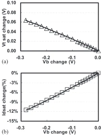
device Vt shift, and circuit functional failure. The impact of the BBL on device characteristics can be studied by using the SPICE simu-lation. A two-step SPICE simulation is used to evaluate the Vt shift caused by the BBL current. The first step is to obtain the Vt change caused by the Vb variation. The second step is to obtain the Vb change caused by the BBL current. Figure3shows SPICE simula-tion results of Idsat and Vtsat characteristics as funcsimula-tions of Vb. For nMOSFETs, when Vb is decreased by 50 mV due to BBL, Vtsat is increased by 13 mV and Idsat is decreased by 2.25%, as shown in Fig.3. The BBL induces Vb change that could cause variations in Vt and Idsat. From the results, it is important to minimize the BBL current in PD-SOI devices to below the S/D junction leakage cur-rent; otherwise, Vt and Idsat of stack devices might become unpre-dictable during circuit operation.
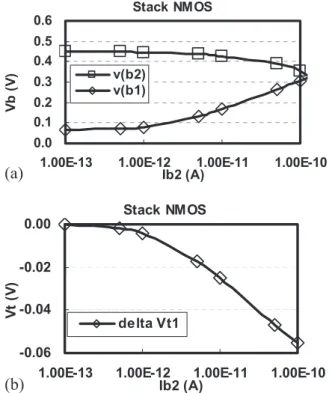
In a PD-SOI technology, each device is isolated from its neigh-boring devices by BOX and shallow trench isolation. Only stack devices can be affected by the BBL. Figure4illustrates the sche-matic circuit diagram of the two stack devices used for the BBL characterization. The BBL current is denoted as Ib2. If the BBL does not exist, the body potentials, Vb1 and Vb2, are 0.432 and 0.055 V, respectively. If the BBL exists between the two stack devices, the BBL current can affect the body potentials共Vb1 and Vb2兲 and Vt1, as shown in Fig. 5. As Ib2 increases, the changes in Vb and Vt become more noticeable. Vb2 is less sensitive to the BBL compared to Vb1 because of its higher forward junction leakage compared to the BBL. The impact of Vb2 is not significant until the BBL current is high enough to about forward junction level. To prevent circuit failure caused by the Vb shift, the BBL current must be minimized.
Dependence of BBL on layout effect.— To fully characterize the
BBL behavior in PD-SOI devices, the layout effect must be taken into consideration. The BBL has been measured on a set of test structures with variations in the PS, device width, and device length. The BBL current increases exponentially as the PS is decreased, as shown in Fig.6a. The BBL current is basically independent of polywidth and length, as shown in Fig.6bandc. The S/D junction becomes shallower for a smaller PS device due to the shadowing effect of implants. When the technology migrates from 45 nm共PS is 140 nm兲 to 32 nm 共PS is 100 nm兲, the PS and the S/D junction depth
are scaled down proportionally with the gate length. The BBL cur-rent shows a drastic increase of more than 1000 times when the polyspace is decreased from 180 to 108 nm. The BBL issue becomes one of the scaling limitations for PD-SOI devices.
(a)
(b)
-15%
-12%
-9%
-6%
-3%
0%
-0.3
-0.2
-0.1
0.0
Vb change (V)
Ids
a
t
c
h
a
nge
(%
)
0.00
0.02
0.04
0.06
0.08
0.10
-0.3
-0.2
-0.1
0.0
Vb change (V)
V
t
s
a
t
c
ha
nge
(V
)
Figure 3. 共a兲 SPICE simulation results for nMOSFET. When Vb is
de-creased, Vtsat is increased.共b兲 When Vb is decreased, Idsat is decreased. 1E-12 1E-10 1E-08 1E-06 1E-04 1E-02 1E+00 -40 -30 -20 -10 0 10 20 30 40 Vbg (V) B B L c ur re nt (A .U .) low Vb2 high Vb2
Figure 2. The BBL is a function of back-gate bias. When a positive Vbg is
applied, the BBL is smaller because the depletion layer width of the S/D junction is wider. When a negative Vbg is applied, the BBL becomes larger and the isolation between the two stack devices becomes worse because the junction depth is reduced.
Schematic for Vb Simulation
Vn1
Vg1=0
Vb2=0.055V
Vn2
Vn3=Vdd
Ib2
Vb1=0.432V
Figure 4. Schematic circuit diagram of the two stack devices. The BBL
current is denoted as Ib2. The body potentials, Vb1 and Vb2, are 0.432 and 0.055 V, respectively, when the BBL does not exist.
For our technology having multiple Vt devices, the BBL current of high threshold voltage 共HVt兲 devices is about 25 times higher than that of standard threshold voltage 共SVt兲 devices. The higher well doping in HVt devices creates a leakage path under the S/D junction; therefore the BBL current is higher.
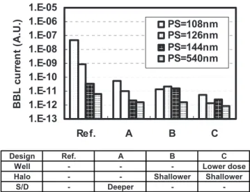
BBL minimization.— Figure 7 shows the optimization flow to reduce the BBL current. Physical dimensions of a device are gener-ally reduced to 70% from 65 to 45 nm node by following the scaling rules. When scaling down PD-SOI devices, the BBL becomes a serious concern because we scale up well doping and scale down the PS 共from 200 to 140 nm兲, but the SOI layer thickness is barely changed to maximize mobility enhancement from the e-SiGe stres-sor. We have demonstrated that the BBL current could be minimized through implant optimization. If the S/D junction abuts the BOX, the BBL current can be greatly reduced. Figure8 shows that the BBL current can be reduced by optimizing the implant conditions of the S/D, halo, and well implants. Design A shows that the BBL current can be reduced by increasing the S/D junction depth. Design B shows that the BBL current can be reduced by reducing the halo implant energy. The BBL current can be further reduced in Design C by optimization of the halo, well, and S/D implants. By implant optimization, the minimum allowable PS can be reduced from 540 to 108 nm.
The BBL effect is highly dependent on the SOI thickness, as shown in Fig.9. Wafers were fabricated using three different SOI thicknesses共Reference, 70 Å less, and 140 Å less兲. The thinner SOI layer allows shallower S/D junctions to abut the BOX and has a weaker dependence on the PS.
The dopant diffusivity also plays an important role in the BBL effect. In an advanced technology, shallow junctions are typically formed with dopant with low diffusivity. However, the BBL issue becomes more severe for a shallower junction. For pMOSFETs, the BBL effect shows less dependence on the PS because boron has a higher diffusivity than phosphorus. S/D junctions of pFETs formed by boron implant are easier to abut the BOX than the S/D junctions of nFETs formed by phosphorus implant, as shown in Fig.10. In an
advanced technology with e-SiGe S/D stressors, pMOSFETs com-monly have raised the S/D to increase the SiGe volume to boost the device performance and reduce the S/D series resistance. The raised S/D produces shallower junctions even using the same implant en-ergy. Figure11illustrates PS dependence of the BBL current using raised S/D e-SiGe. After optimizing the e-SiGe profile and implant condition, the dependence of the BBL current on the PS can be further reduced. From the experimental results, we have demon-strated that PS dependence of the BBL current at 45 nm node can be reduced by implant optimization, e-SiGe profile improvement, and SOI thickness reduction.
Conclusions
The BBL becomes significant and affects the overall circuit per-formance in PD-SOI as the polypitch is scaled continuously to 32 nm and beyond technology. A methodology for BBL extraction has been demonstrated in this paper. The impact of BBL can be mini-mized by optimizing well, halo, and S/D implantation. The Si thick-Stack NMOS 0.0 0.1 0.2 0.3 0.4 0.5 0.6
1.00E-13 1.00E-12 1.00E-11 1.00E-10 Ib2 (A) Vb (V) v(b2)v(b1)
(a)
(b)
Stack NMOS -0.06 -0.04 -0.02 0.001.00E-13 1.00E-12 1.00E-11 1.00E-10
Ib2 (A)
Vt
(V)
delta Vt1
Figure 5.共a兲 When the BBL exists between two stack devices, Vb1 and Vb2
are changed. As Ib2 increases, the Vb change becomes more noticeable.共b兲 Ib2 leads to device Vt change.
1.E-10 1.E-09 1.E-08 0.108 0.27 0.54 0.9 Width (nm ) B B L c u rr e n t (A .U .) ref 1.E-11 1.E-10 1.E-09 1.E-08 0.036 0.0405 0.054 0.18 Length (nm ) B B L c u rr e n t (A .U .) ref
(a)
(b)
(c)
Figure 6. 共a兲 The BBL increases exponentially as the PS decreases. When
the technology migrates from 45 to 32 nm, the BBL current shows a drastic increase of more than 1000 times. The BBL current of the HVt device is about 25 times higher than that of SVt devices.共b兲 The BBL is not a function of device width.共c兲 The BBL is not a function of device length.
ness of the SOI should be reduced after shrinking the S/D junction depth in future technology. Additionally, higher BBL is also ob-served if a raised S/D structure is employed.
Taiwan Semiconducting Manufacturing Company Ltd. assisted in meet-ing the publication costs of this article.
References
1. I. M. Hafez, G. Ghibaudo, and F. Balestra, IEEE Trans. Electron Devices, 37, 818 共1990兲.
2. K. Kato, T. Wada, and K. Taniguchi, IEEE Trans. Electron Devices, 32, 458 共1985兲.
3. J. P. Colinge, IEEE Electron Device Lett., 9, 97共1988兲.
4. H. Nakayama, M. Nakamura, H. Komatsu, and C. Hu, in SOI Conference, IEEE, pp. 128–129共2000兲.
Design Ref. A B C
Well - - - Lower dose
Halo - - Shallower Shallower
S/D - Deeper - -1.E-13 1.E-12 1.E-11 1.E-10 1.E-09 1.E-08 1.E-07 1.E-06 1.E-05 Ref. A B C B B L c ur re nt (A .U .) PS=108nm PS=126nm PS=144nm PS=540nm
Figure 8. The BBL is reduced by optimizing the implant conditions of the
S/D, halo, and well implants. After implant optimization, the minimum al-lowable PS is reduced from 540 to 108 nm.
1.E-13 1.E-11 1.E-09 1.E-07 1.E-05
Ref. Ref.-70A Ref.-140A
BBL c u rr e n t (A. U .) PS=108nm PS=126nm PS=144nm PS=540nm
Figure 9. The BBL is dependent on the SOI thickness. The thinner SOI layer
allows shallower S/D junctions to abut the BOX and decouple the BBL PS dependence. 1.E-12 1.E-11 1.E-10 1.E-09 1.E-08 1.E-07 1.E-06 1.E-05 108 126 144 180 540 Poly Space (nm ) B B L c u rre n t (A. U .) phosphorus boron
Figure 10. The dopant diffusivity plays an important role in the BBL. For
the pMOSFETs, the BBL shows less dependence in the PS because boron has higher diffusivity than phosphorus and is easier to abut the BOX.
1.E-13 1.E-12 1.E-11 1.E-10 1.E-09 108 126 144 180 540 Poly Space (nm ) BBL c u rr e n t (A. U. ) Raised S/D SiGe
Optim ized SiGe
Figure 11. The PS dependence of the BBL is significant using the raised S/D
e-SiGe. After optimizing the e-SiGe profile and implant condition, the de-pendence of BBL on PS is minimized.
S/D
Poly Spacing
S/D
Poly Spacing and S/D Junction Scaling
S/D
Implant/process OptimizationBBL
65nm
200nm
45nm
140nm
Si thickness
BOX
BOX
BOX
Junction
depth
Figure 7. When scaling PD-SOI devices from 65 to 45 nm technology, the
BBL becomes a concern because we scale up well doping and scale down the PS, but the SOI layer thickness is barely changed to maximize mobility enhancement from the e-SiGe stressor. The BBL could be minimized through implant optimization to make the S/D junction abut the BOX.
5. L. T. Su, J. E. Chung, D. A. Antoniadis, K. E. Goodson, and M. I. Flik, IEEE
Trans. Electron Devices, 41, 69共1994兲.
6. W. Jin, S. K. H. Fung, W. Liu, P. C. H. Chan, and C. Hu, Tech. Dig. - Int. Electron
Devices Meet., 1999, 175.
7. M. R. Casu and P. Flatresse, in SOI Conference, IEEE, pp. 62–63共2002兲. 8. Q. Liang, T. Kawamura, M. Ketchen, S. Kawanaka, M. M. Pelella, D. Robertson,
M. Bhushan, K. Mcstay, G. Freeman, K. Miyamoto, et al., in SOI Conference, IEEE, pp. 95–96共2006兲.
9. F. Assaderaghi, G. G. Shahidi, L. Wagner, M. Hsieh, M. Pelella, S. Chu, R. H. Dennard, and B. Davari, IEEE Electron Device Lett., 18, 241共1997兲.
10. A. Wei and D. A. Antoniadis, IEEE Electron Device Lett., 17, 193共1996兲. 11. M. Ieong, R. Young, H. Park, W. Rausch, I. Yang, S. Fung, F. Assaderaghi, and
H.-S. P. Wong, in SISPAD, IEEE, pp. 230–232共2001兲.
12. H. C. Lo, W. C. Luo, W. Y. Lu, C. F. Cheng, B. Wu, T. L. Chen, C. H. Lien, S. K. H. Fung, and H. C. Tuan, in SOI Conference, IEEE, pp. 49–50共2008兲. 13. P. R. Chidambaram, B. A. Smith, L. H. Hall, H. Bu, S. Chakravarthi, Y. Kim, A. V.
Samoilov, A. T. Kim, P. J. Jones, R. B. Irwin, et al., Tech. Dig. - Int. Electron
Devices Meet., 2004, 48共2004兲.
14. S. E. Thompson, M. Armstrong, C. Auth, M. Alavi, M. Buehler, R. Chau, S. Cea, T. Ghani, G. Glass, T. Hoffman, et al., IEEE Trans. Electron Devices, 51, 1790
共2004兲.
15. P. Grudowski, X.-Z. Bo, V. Adams, K. Loiko, D. Tekleab, S. Filipiak, J. Hacken-berg, V. Kolagunta, M. Foisy, L.-T. Lin, et al., in SOI Conference, IEEE, pp. 19–20 共2006兲.
16. K. V. Loiko, V. Adams, D. Tekleab, B. Winstead, X. Z. Bo, P. Grudowski, S. Goktepeli, S. Filipiak, B. Goolsby, V. Kolagunta, et al., in SISPAD, IEEE, pp. 123–126共2006兲.
17. C.-H. Chen, T. L. Lee, T. H. Hou, C. L. Chen, C. C. Chen, J. W. Hsu, K. L. Cheng, Y. H. Chiu, H. J. Tao, Y. Jin, et al., Dig. Tech. Pap. - Symp. VLSI Technol., 2004, 56.
18. C. Ortolland, P. Morin, C. Chaton, E. Mastromatteo, C. Populaire, S. Orain, F. Leverd, P. Stolk, F. Boeul, and F. Arnaud, Dig. Tech. Pap. - Symp. VLSI Technol.,
2006, 78.
19. D. V. Singh, J. W. Sleight, J. M. Hergenrother, Z. Ren, K. A. Jenkins, O. Dokumaci, L. Black, J. B. Chang, H. Nakayama, D. Chidambarrao, et al., Tech. Dig.
-Int. Electron Devices Meet., 2005, 505.
20. S. K. H. Fung, H. C. Lo, C. F. Cheng, W. Y. Lu, K. C. Wu, K. H. Chen, D. H. Lee, Y. H. Liu, I. L. Wu, C. T. Li, et al., Tech. Dig. - Int. Electron Devices Meet., 2007, 1035.