S0013-4651(98)08-119-1 CCC: $7.00 © The Electrochemical Society, Inc.
Owing to its anisotropic etching ability, reactive ion etching (RIE) is extensively used to etch silicon oxide to form contact holes or interconnect vias. However, because of inevitable energetic ions and fluoride radicals in the plasma ambient, RIE causes damage, defects, polymer residue, and radical contamination1-5 on etched surfaces, and induces oxide traps in the SiO2or interface states at the SiO2/Si interface.6-8 Therefore, the reverse current, contact resis-tance, and oxide leakage of devices are inevitably enlarged due to the undesirable effects described previously.5,9,10,11 Currently, the issue of RIE selectivity has become increasingly critical in ultra-shallow junctions because overetch is less tolerated. To alleviate these problems on RIE-etched silicon surfaces, several modified and complex dry-etching techniques, e.g., magnetically enhanced reac-tive ion etching (MERIE),2,12 and electron cyclotron resonance (ECR) plasma etching,10,13 have been developed. Many different etchant sources, e.g., CF4, CHxF42x, NF3, SF6, SiF4, BCl3, and HBr etc., have also been developed to increase etching selectivity or re-duce the effects of impurities and defects on the etched surface.14 Several severe postcleaning and post-treatment methods after RIE have also been developed to remove damage or polymer resi-dues.5,15-17Although these post-treatment techniques have been im-proved once again and the RIE apparatuses have gradually become extremely expensive, RIE cannot be compared with conventional wet-etching in the integrity of the etched surface.9,10,16In addition, to improve the overetch problem, many techniques, e.g., laser inter-ferometry, optical emission spectroscopy (OES), invasive Langmuir probes, and radio-frequency power monitoring, have been developed as an end-point detector.18-20Despite additional equipment and high cost, each proposed technique has drawbacks and limitations.
To avert these problems, an alternative method without RIE etch-ing must be developed. Our previous studies have investigated liq-uid-phase deposition (LPD) technology,21-24and applied it to the gate insulator of thin-film transistors (TFTs).25,26Many physical and chemical characteristics, such as Auger electron spectroscopy (AES) analysis,21,22Fourier transform infrared (FTIR) spectra,22,24X-ray photoelectron spectroscopy (XPS) measurement,24 extraction of interface trap,25film stress measurement,23stress hysteresis,23etc., for LPD dielectric films have been surveyed and analyzed in our pro-posed papers.21-25The LPD technique has also been applied to form the interlayer dielectric (ILD) in multilevel tungsten interconnect structures.28These studies confirm that LPD oxide possesses excel-lent electrical properties, low dielectric constant (k)22 and low stress.23Due to low stress, LPD oxide exhibits fewer trap states than plasma-enhanced chemical vapor deposited (PECVD) oxide at the oxide/Si interface.23,25,27This reveals there is a better interface state
between silicon and LPD oxide than conventional PECVD oxide. Especially, LPD oxide can be selectively deposited against photore-sist if the deposition condition is adequately controlled.29,30 This implies the feasibility of applying selective LPD (S-LPD) to create contact holes or vias. In addition, the cost of LPD apparatus is quite low, because no vacuum facilities and no corresponding etching monitors are necessary. In this work, we first apply S-LPD to form contact holes for n1/p diodes, Schottky diodes, and Kelvin resistors and thereby study the superiority of utilizing plasma-free S-LPD over the conventional RIE. It is expected that in addition to forming contact holes with submicron meter scale as RIE, S-LPD can also obtain device performance comparable to wet etching.
Experimental
The process and mechanism of S-LPD have been described in our previous literatures.29-31 Figure 1a indicates that the process window of S-LPD is a function of silicic acid Si(OH)4concentration and deposition temperature. In this work, we mainly perform the S-LPD under a condition at Si(OH)4 concentration of 7.3 3 1023 mol/L and 238C. The SEM photograph in Fig. 1b shows the LPD oxide is selectively deposited against photoresist. It preliminarily reveals the absence of particles and indicates the feasibility of form-ing half-micrometer contact holes with a high aspect ratio.
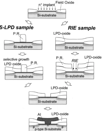
The devices, including n1/p diodes, Schottky diodes, and Kelvin resistors, were fabricated with their contact holes prepared using S-LPD and RIE, respectively. The p-type (100) wafers with 15-25 V cm bulk resistivity were adopted in the n1/p diodes and Kelvin resis-tor fabrication. Following the formation of channel stopper and field oxide, phosphorus with a dose of 5 3 1015cm22and energy of 40 keV was implanted to make n1/p junction, and then the 30 min annealing at N2 9008C was performed for dopant activation. As shown in the left portion of Fig. 2, for S-LPD samples the photore-sist on the area defined as the site of contact hole was kept intact. Next, the LPD oxide was selectively grown on the region without photoresist by using S-LPD. After removing the photoresist, the con-tact holes were automatically formed. For RIE samples, as shown in the right portion of Fig. 2, LPD oxide was globally deposited to cap the n1/p diodes. Then the contact holes were defined through litho-graphy and etched using RIE. To increase the etching selectivity of SiO2/Si14 and reduce chamber particles,32the RIE was performed under the following conditions: a CHF3/O2, ratio of 20/5 sccm, 50 mTorr pressure , and 100 W rf power. Before metallization, the contact holes of both S-LPD and RIE were cleaned sequentially with H2SO4/H2O2, NH4OH/H2O2, HCl/H2O2, and diluted HF solution (standard RCA cleaning). In addition to Al/Si contact, for some sam-ples, 20 nm thick titanium was used between Al and Si to serve as a titanium silicide barrier to reduce spiking. The purpose of using a
Application of Selective Liquid-Phase Deposition to Fabricate Contact
Holes Without Plasma Damage
Ching-Fa Yeh,
zChien-Hung Liu, and Jwinn-Lein Su
Department of Electronics Engineering and Institute of Electronics, National Chiao-Tung University, Hsinchu, Taiwan
This work develops an alternative method, selective liquid-phase deposition (S-LPD), to fabricate contact holes instead of reactive ion etching. In preliminary experiments, deep n+/p junction diodes with contact holes prepared by S-LPD exhibit much less reverse
current, unity ideality factor, larger forward current, lower contact resistance, and higher thermal stability than those prepared by reactive ion etching. Further superiority of plasma damage-free near-surface regions is also investigated using Schottky and ultra-shallow junction diodes. Experimental results indicate that S-LPD can be applied to the submicron contact-hole process. The data after reverse bias temperature stress reveals the satisfactory reliability of LPD contact holes. This work demonstrates that the S-LPD technology is a highly promising means of replacing reactive ion etching processes to form submicron contact holes as reli-ably as those by wet-etching.
© 1999 The Electrochemical Society. S0013-4651(98)08-119-1. All rights reserved. Manuscript submitted August 31, 1998; revised manuscript received February 17, 1999.
Journal of The Electrochemical Society, 146 (6) 2294-2299 (1999) 2295 S0013-4651(98)08-119-1 CCC: $7.00 © The Electrochemical Society, Inc.
single Ti barrier is due to low resistance with respect to using TiN/Ti barrier or Al:Si(1-2%) alloy. Especially for Al:Si/n1-Si contact, an undesirable increase in contact resistance arises from silicon precip-itates which occur preferentially around the contact hole edges.33 After metallization, some n1/p junction diodes were sintered at 4008C for 30 min in N2. The temperatures of all processes after S-LPD are below 5008C, the outgassing temperature of fluorine in LPD dielectric,22so there is no effect due to fluorine outgassing. In addition to n1/p diodes, the Kelvin resistors were also fabricated under an identical conditions. For Schottky diodes, the fabrication procedures closely resembled those of n1/p diodes except for use of 1-5 V cm, n-type (100) wafers and the fact that no ion-implantation was necessary.
Subsequently, we further applied S-LPD to the ultrashallow n1/p junction diodes. All processes closely resembled those mentioned previously except (i) the n1region was prepared with 5 keV, As1, 23 1015 cm22, and then annealed with rapid thermal annealing (RTA) in the N2ambient. (ii) For the RIE sample, the partial-RIE (P-RIE) was employed to etch contact holes. The P-RIE refers to a sit-uation in which most of the capping oxide thickness was etched with RIE and then the remaining oxide of about 20-30 nm was wet-etched by buffer HF solution. This modification attempts to reduce the RIE overetch, because etching rate nonuniformity easily leads to overetch-through in ultrashallow junctions. (iii) To resemble the common RIE process, P-RIE samples were prepared by using
plas-ma-enhanced chemical vapor deposited tetraethylorthosilicate (PE-TEOS) oxide as a capping layer. The PE-TEOS oxide was deposited in the TEOS/O2ratio of 10/200 sccm, 300 mTorr pressure, and 200 W power. (iv) Titanium thickness of all ultrashallow n1/p diodes was reduced to 12 nm.
Results and Discussion
n1/p junction diode.—Figure 3 shows the typical current-voltage
(I-V) characteristics of n1/p diodes with contact holes prepared by S-LPD and RIE before and after sintering, respectively. The metal contact of Al/n1-Si is 60 3 60 mm, while the junction area is 100 3 100 mm. According to this figure, before sintering the reverse cur-rent of S-LPD samples is one order less than that of RIE. As for the forward bias, the ideality factor,h, of 1.13 in S-LPD samples is also superior to that of 1.57 in RIE samples. This indicates that relative-ly few generation-recombination (G-R) centers are in the depletion region of S-LPD diodes such that h approaches 1. Table I summa-rizes several key characteristic parameters. The reverse current ratio of 400 3 400 mm diodes to 100 3 100 mm diodes (I400/I100) is 3.27 for the S-LPD sample, while it is 5.15 for the RIE sample. The
I400/I100 ratio of 5.15 exceeds the geometry ratio of the junction perimeter, i.e., 1600/400 mm 5 4. From the fitting with the equation
IR5 JRA3 L21 JRP3 (4L), where JRAand JRPare the partial cur-rent densities due to junction area leakage and junction periphery leakage, respectively, the factor of I400/I100> 4 indicates that the effect of JRA is rather significant for the RIE sample. The RIE method easily causes lattice defects and bonding defects, which function as deep-level traps1,34 and donor-like charge states,35 respectively. For the contact etched by CHF3, it has been detected by deep-level transient spectroscopy (DLTS) that a dominant trap aris-es from H(0.40) Si defects and locataris-es at about 0.65 eV above the valence band.1These states and traps serve as G-R centers and sig-nificantly enlarge the reverse current. In addition, fluorine-contained ion bombardment and permeation also cause soft breakdown.36 These factors account for why the reverse current is rather high for
Figure 1. (a) Process window and (b) SEM photograph for S-LPD.
Figure 2. Process-flow diagram of n1/p junction diodes with contact hole fabricated by S-LPD (left) or conventional RIE (right).
S0013-4651(98)08-119-1 CCC: $7.00 © The Electrochemical Society, Inc.
RIE samples. After sintering, the reverse current of RIE samples increases drastically. This large leakage magnitude after sintering indicates a spiking enhanced by RIE damage. It has been proposed that RIE can damage the etched surface to become as rough as 30 nm and makes the spiking effect easily occur during sintering treat-ment.5In contrast, S-LPD can avoid a large reverse current owing to no plasma-induced defects and no energetic ion bombardment dam-ages during contact hole formation.
Figure 4 shows the performance of S-LPD and RIE diodes with Al/Ti/Si contact, respectively. Before sintering, the I-V characteristics of S-LPD samples are still superior to those of RIE samples. After sin-tering, both the reverse currents increase, while RIE samples increase more significantly than S-LPD samples. This can be attributed to many defects and contamination induced by RIE diffusing from con-tact-hole surfaces into the junction depletion region during sintering. In particular, the metallic contamination sputtered from the RIE chamber wall enlarges reverse current after sintering.37Having no such drawbacks, the S-LPD samples exhibit relatively good thermal stability. Figure 5 shows the accumulative distribution for the reverse
currents of all measured diodes. For S-LPD samples, the reverse cur-rents distribute in a more confined region; however, for RIE samples, they separate from nanoampere to microampere magnitude. This find-ing indicates another superiority that S-LPD has no nonuniformity problem of RIE etching rate.38So far, applying S-LPD can avoid the problem of defects, contamination, rough-etched surfaces, and etch-ing rate nonuniformity caused by RIE. These results preliminarily prove the superiority of S-LPD replacing RIE to form contact holes.
Ohmic contact resistance.—According to Fig. 3 and 4, the
for-ward current of S-LPD samples is larger than that of RIE samples at forward bias 21.0 V, whether a titanium barrier is used or not. This implies that applying S-LPD can effectively reduce forward series resistance. Because all processes are the same except the contact-hole formation, it is believed that for RIE samples, the additional resistance must result from contact resistance. To investigate contact resistance, we further fabricated four-terminal Kelvin D-resistors,39 as illustrated in the Fig. 6 inset. The n1doping region of sheet resis-tance 25.5 V/u was adopted for all resistors. The Kelvin contact
Figure 3. Comparison of I-V characteristics between n1/p diodes with S-LPD and RIE contact (Al/Si) holes.
Table I. Comparison for key characteristic parameters of diodes and ohmic contacts between S-LPD and RIE contact holes.
S-LPD RIE
n1/p diode
Ideality factor h (Al/Si) 1.13 1.57
(20.4 to 20.5 V)a
Dimension current ratio 3.27 5.15
I400/I100(5.0 V) a
Ideality factor h (Al/Ti/Si) 1.17 1.64
(20.4 to 20.5 V) Ohmic Contact resistivity rce 2.5 3 1026 ,12 3 1026 (V cm2) b Schottky diode Schottky hsc(0.1-0.3 V) 1.11 >3.0
Schottky barrier height (eV) 0.83 0.60
Ultrashallow n1/p diode
Ideality factor h (20.4 to 20.5 V) 1.03 1.13c a Diodes with Al/Si contact considered before sintering.
b Sheet resistance, R
s, 25.5 V/u. c P-RIE was adopted.
Figure 4. Comparison of I-V characteristics between n1/p diodes with S-LPD and RIE contact (Al/Ti/Si) holes before and after sintering.
Figure 5. Cumulative distribution for reverse currents, at reverse bias 5.0 V, of all measured S-LPD and RIE n1/p diodes before and after sintering.
Journal of The Electrochemical Society, 146 (6) 2294-2299 (1999) 2297 S0013-4651(98)08-119-1 CCC: $7.00 © The Electrochemical Society, Inc.
resistance, RC, is defined by the voltage 2 to 4 over the fed current 1-3, i.e., the curve slope of V24-I13plot. Figure 6 depicts the typical RCcharacteristics of the resistor with the contact size L 3 L 5 10 3 10 mm and the collar width d 5 10 mm at the fed current ranging from 24 to 4 mA. The S-LPD contact shows a linear I-V relation-ship and exhibits a smaller RCthan the RIE contact. Meanwhile, the RIE contact shows a nonlinear I-V relationship and therefore exhibits a nonconstant and larger RCvalue, especially at the small fed current. This occurrence is because in the RIE process, the poly-mer and photoresist residues are difficult to be cleaned owing to the energetic plasma bombardment.5In addition, the large RCcan also be attributed to the decreased mobility in the etched surface.40 Inter-estingly, the impurities and residues impinged by RIE scatter the drift electrons and holes, thereby reducing the effective mobility. Owing to the scattering, the drift carriers are scattered rather seri-ously if they move at a low velocity. This is the reason the RCof RIE contact becomes large, particularly in small fed current, and exhibits nonlinear I-V characteristics. For S-LPD contact, it is relatively easy to clean the photoresist residues because of no energetic bombard-ment. Therefore, the I-V characteristics show linearity with low slope and exhibit the superiority of being plasma-damage free.
Figure 7 depicts the relationship between contact resistance, RC, and different contact-hole sizes for the S-LPD and RIE samples. According to this figure, the S-LPD contacts always exhibit a lower contact resistance than the RIE ones for all contact-hole sizes. In addition, compared to RIE contacts, the RCreduction has a tenden-cy of becoming more apparent in small contact-hole sizes. On the other hand, the RCvalues vs. the contact-hole sizes exhibit a linear trend with about 21 slope, regardless of whether for S-LPD or RIE samples. This indicates that our Kelvin resistors can eliminate most of the parasitic resistance and thus can be used to extract specific contact resistivity, rCe, and make rCe close to the actual contact resistivity rC.39To extract the rCe, we incorporate the measured RC values with different L/d ratio into the simulated universal curves of Kelvin D-resistors. As shown in Fig. 8, for resistors with different
L/d ratios, the RC/RSvalues of S-LPD samples are much smaller than those of RIE samples. Following the extraction procedures of rCe,41 the specific Al/Si contact resistivity,rCe, as listed in Table I, is about 2.5 3 1026V cm2for the S-LPD contacts; however, it is about 12-13 3 1026V cm2for the RIE contacts. Because the contact resis-tivity is very sensitive to the cleanness and integrity at the metal/Si interface, the specific rCeof RIE must be larger than that of S-LPD. Schottky diodes and ultrashallow n1/p junction diodes.—Now
that the S-LPD method has been preliminarily shown feasible to
replace RIE in contact-hole formation, especially in damage-free and contamination-free processes to further prove its excellence without plasma, the performance in near-surface regions is next investigated thru Schottky and ultrashallow junction diodes.
Schottky diodes.—Figure 9 depicts the performance of S-LPD
and RIE Schottky diodes with Al/n-Si (1-5 V cm) contact be-fore/after N24008C sintering, and Table I also summarizes their key characteristic parameters. Before sintering, the RIE sample nearly loses the rectifying characteristics of a Schottky diode under reverse bias, while the S-LPD sample exhibits satisfactory Schottky charac-teristics. However, after sintering, the S-LPD sample still exhibits about four orders smaller than that of RIE sample in reverse current. Meanwhile, the ideality factor 1.11 of the former is lower than 4.05 of the latter. The worse ideality of RIE samples is attributed to the large surface recombination velocity.42According to the curves of ln{I/[1 2 exp(2qV/kT)]} vs. forward-bias voltage, the potential bar-rier is 0.83 eV for the S-LPD Schottky diodes and 0.60 eV for the RIE ones, respectively. As generally contended, the donor-like bond-ing defects and the polymer residues make the depletion region
Figure 6. V-I plot of Kelvin D-resistors with S-LPD and RIE contact holes, respectively.
Figure 7. Comparison of contact resistance, RC, between S-LPD and RIE contact holes for different contact sizes.
Figure 8. Measured RC/RSwithin simulated universal curves for the Kelvin D-resistors with S-LPD and RIE contact holes, respectively.
S0013-4651(98)08-119-1 CCC: $7.00 © The Electrochemical Society, Inc.
thin43and lower the potential barrier. These results indicate that for the RIE Schottky diodes, the sintering is essential to release some of the residues and the defects from the Si surface but is unnecessary for the S-LPD sample. Accordingly, the RIE process becomes more critical and requires additional post-treatment.16 S-LPD can avert these problems and is indeed a highly promising candidate as a plas-ma-damage-free, energetic-impurity-free, and polymer-residue-free technology.
Ultrashallow n1/p junction diodes.—Because the demand for
plasma-damage free technology has been increasingly urgent in fab-ricating deep submicron devices, the S-LPD technique was next applied to the formation of contact holes for ultrashallow n1/p junc-tions. Herein, the junction depth estimated with TSUPRUM-4 is about 20-30 nm, while the implantation of 5 keV As1, 2 3 1015cm22 is adopted, and following with 15 s, 10508C RTA. While fabricating the ultrashallow junction diodes, the RIE samples were modified by applying PE-TEOS capping and partial-RIE (P-RIE). Meanwhile, to segregate all lithography residues from the contact region, a simple modification of S-LPD was performed with a thin LPD-oxide (15-20 nm) globally deposited before lithography, as illustrated in the Fig. 10 inset. After finishing S-LPD and removing the photoresist, the thin LPD oxide was removed by dipping buffer HF solution and then the contamination-free contact holes were formed. Besides the large area samples with the Al/Ti/n1-Si contact area of 60 3 60 mm and the n1/p junction area of 100 3 100 mm, the submicron samples with junction area of 2.8 3 50 mm and 25 contact holes of 0.8 3 0.8 mm were also fabricated. Photoresist removal and cleaning for the submi-cron samples was performed by 60 s ozone ashing of 3008C and fol-lowed by RCA cleaning. In addition to S-LPD and P-RIE, the refer-ence samples (wet-etch) with LPD-oxide capping and completely butter HF wet-etching were also prepared.
Figure 10 shows the typical I-V characteristics of ultrashallow junction diodes with 60 3 60 mm contact holes prepared by S-LPD, wet-etch, and the P-RIE method, respectively, after sintering. The S-LPD diodes as well as wet-etch reference diodes exhibit nearly iden-tical I-V characteristics in both forward bias and reverse bias. This proves that applying S-LPD can form excellent diodes comparable to the wet-etch reference diode. By contrast, the P-RIE diodes still exhibit two orders higher reverse current than the S-LPD ones at 5.0 V. This can be attributed to some energetic ions or accelerated radicals penetrating through the 20-30 nm remaining oxide into the Si substrate. In addition, the microtrenching effect44 due to ion reflection from the photoresist sidewall also causes overetch at the
contact periphery and enhanced penetration. However, these unde-sirable problems never occur in the S-LPD diodes.
Figure 11 shows the accumulative reverse-current distribution of all measured S-LPD diodes and P-RIE diodes at reverse bias 2.5 V. All reverse currents of S-LPD diodes accumulate at about several picoam-pere magnitude either before or after sintering. In addition, the S-LPD diodes after sintering show slightly lower reverse currents than those before sintering. This is consistent with the proposed results of Ti-sili-cide contact reducing reverse current after thermal treatment.45,46For the P-RIE diodes, exhibit not only high reverse currents but also great-ly increase to 1024Å after sintering. This reveals that the titanium occasionally loses its barrier effect in some P-RIE diodes, yet this fail-ure does not occur in all S-LPD diodes. Cumulatively, our results demonstrate that even if P-RIE has been adopted to avoid overetch-ing, S-LPD samples are still superior to P-RIE samples.
Figure 12 shows the typical diode I-V characteristics of the submi-cron samples. The satisfactory forward and reverse current reveal the complete cleaning for the photoresist of S-LPD samples by combining
Figure 9. Comparison of I-V characteristics between Schottky diodes with S-LPD and RIE contact holes, before and after sintering (Al/n-Si contact area
5003 500 mm).
Figure 10. Comparison of I-V characteristics among ultrashallow n1/p junc-tion diodes with S-LPD, wet-etch (LPD), and P-RIE (PE-TEOS) contact holes (Al/Ti/Si contact) after sintering.
Figure 11. Cumulative distribution for reverse currents, at reverse bias 2.5 V, of all measured S-LPD and P-RIE ultrashallow n1/p junction diodes before and after sintering.
Journal of The Electrochemical Society, 146 (6) 2294-2299 (1999) 2299 S0013-4651(98)08-119-1 CCC: $7.00 © The Electrochemical Society, Inc.
ozone ashing and RCA cleaning. The extremely low reverse leakage proves the superiority of applying S-LPD instead of RIE to 0.8 mm contact hole formation. These results indicate that S-LPD can be applied to the submicron contact hole processes. A reverse bias (15.0 V) and temperature (1758C) stress (RBTS)47was imposed on the S-LPD submicron samples for reliability examination. After stress of 96 h, shown as the dash-dot line in Fig. 12, junction leakage is still kept at very low leakage magnitude (2.8 pA) and is indeed lower than the leakage of the RIE submicron sample before RBTS. This reliability is much better than the proposed results47and indicates that a stable TiSi2 structure is formed in LPD contact. Our RBTS results suggest S-LPD as a satisfactory method for reliable contact hole formation.
Conclusion
We have successfully applied the novel S-LPD method to form submicron contact holes and investigated its superiority through n1/p diodes, Kelvin contact resistors, and Schottky diodes. The S-LPD n1/p diode is superior to the conventional RIE diode with respect to its low reverse current, unity ideality factor, good thermal stability, low contact resistivity, and no problem of etching-rate nonuniformity. Compared with the RIE Schottky diode, the S-LPD Schottky also exhibits excellent rectifying characteristics with high potential barrier, 0.83 eV. The S-LPD ultrashallow junction diodes as well as wet-etch reference diodes show nearly identical I-V charac-teristics. The similar superiority of S-LPD also exists in our submi-cron samples. RBTS results suggest S-LPD as a method for reliable contact hole formation. In sum, the S-LPD technique has overcome many undesirable problems induced by RIE. That is, the S-LPD method indeed has the following superiorities in forming contact holes or vias for scaled-down devices: (i) it is a plasma-free process; (ii) it is a damage-free process; and (iii) it is a particle, residue, and contamination-free process. Accordingly, the S-LPD is a promising alternative for replacing conventional RIE for contact hole or via for-mation. In addition, LPD apparatus costs very little because no vac-uum, power, gas-flow equipment, and corresponding etching moni-tors are needed. Therefore, we believe that in near future, the novel S-LPD method is a good candidate for fabricating the contact holes of deep-submicron devices without plasma damage to fulfill more reliable and more cost-effective requirements in ULSI technologies.
Acknowledgment
The authors thank the National Science Council of the Republic of China for financially supporting this research under contract no. NSC 88-2215-E009-036.
National Chiao-Tung University assisted in meeting the publication costs of this article.
References
1. O. O. Awadelkarim, P. I. Mikulan, T. Gu, R. A. Ditizio, and S. J. Fonash, IEEE Electron Device Lett., EDL-15, 85 (1994).
2. O. O. Awadelkarim, T. Gu, R. A. Ditizio, P. I. Mikulan, S. J. Fonash, J. F. Rembet-ski, and Y. D. Chan, IEEE Electron Device Lett., EDL-14, 167 (1993). 3. R. G. Frieser, F. J. Montillo, N. B. Zingerman, W. K. Chu, and S. R. Mader, J.
Elec-trochem. Soc., 130, 2237 (1983).
4. M. Ephrath and R. S. Bennett, J. Electrochem. Soc., 129, 1822 (1982). 5. Y. Wang, S. W. Graham, L. Chan, and S. T. Loong, J. Electrochem. Soc., 144, 1522
(1997).
6. R. L. Guldi and D. R.Wyke, J. Electrochem. Soc., 143, 628 (1996).
7. A. Tsukamoto, K. Mizushima, Y. Hidaka, H. Okada, and S. Terakawa, Jpn. J. Appl. Phys., 32, 3058 (1993).
8. B. Y. Tsui, S. H. Liu, G. L. Lin, J. H. Ho, C. H. Chang, and C. Y. Lu, IEEE Elec-tron Device Lett., EDL-16, 64 (1995).
9. D. Misra and E. L. Heasell, J. Electrochem. Soc., 136, 234 (1989).
10. H. Kimura, K. Shiozawa, K. Kawai, H. Miyatake, and M. Yoneda, Jpn. J. Appl. Phys., Part 1, 34, 2114 (1995).
11. S. Fang and J. P. McVittie, IEEE Electron Device Lett., EDL-13, 288 (1992). 12. H. H. Goto, T. Ohmi, H-D. Lowe, K. Y. Fung, and S. G. Newberry, IEEE Trans.
Semicond. Manufact., TSM-5, 337 (1992).
13. K. T. Sung, S. W. Pang, M. W. Cole, and N. Pearce, J. Electrochem. Soc., 142, 206 (1995).
14. D. R. Sparks, J. Electrochem. Soc., 139, 1736 (1992).
15. K. Ueno, V. M. Donnelly, and T. Kikkawa, J. Electrochem. Soc., 144, 2565 (1997). 16. H. C. Tseng, C. Y. Chang, F. M. Pan, and L. P. Chen, J. Appl. Phys., 78, 4710
(1995).
17. J. P. Simko, G. S. Oehrlein, and T. M. Mayer, J. Electrochem. Soc., 138, 277 (1991).
18. M. Sternheim, W. van Gelder, and A. W. Hartman, J. Electrochem. Soc., 130, 655 (1983).
19. P. J. Marcoux and P. D. Foo, Solid State Technol., 99, (April 1981).
20. H. L. Maynard, E. A. Rietman, J. T. C. Lee, and D. E. Ibbotson, J. Electrochem. Soc., 143, 2029 (1996).
21. C. F. Yeh, C. L. Chen, and G. H. Lin, J. Electrochem. Soc., 141, 3177 (1994). 22. C. F. Yeh and C. L. Chen, J. Electrochem. Soc., 142, 3579 (1995). 23. C. F. Yeh, S. S. Lin, and W. Lur, J. Electrochem. Soc., 143, 2658 (1996). 24. C. F. Yeh, C. L. Chen, W. Lur, and P. W. Yen, Appl. Phys. Lett., 66, 938, (1995). 25. C. F. Yeh, S. S. Lin, T. Z. Yang, C. L.Chen, and Y. C.Yang, IEEE Trans. Electron
Devices., ED-41, 173 (1994).
26. C. F. Yeh, T. Z. Yang, and T. J.Chen, IEEE Trans. Electron Devices, ED-42, 307 (1995).
27. C. F. Yeh, S. S. Lin, and T. Y. Hong, IEEE Electron Device Lett., EDL-16, 316 (1995).
28. T. Homma, T. Katoh, Y. Yamada, and Y. Murao, J. Electrochem. Soc., 140, 2410 (1993).
29. C. F. Yeh and C. L. Chen, Semicond. Sci. Technol., 9, 1250 (1994).
30. C. F. Yeh, Y. C. Lee, and J. L. Su, in Proc. SPIE - Int. Soc. Opt. Eng., 2879, 260 (1996).
31. C. F. Yeh and C. H. Liu, in Proceedings on Plasma Process Induced Damage (98’P2ID), p. 223, American Vacuum Society (1998).
32. M. M. Smadi, G. Y. Kong, R. N. Carlile, and S. E. Beck, J. Electrochem. Soc., 139, 3356 (1992).
33. S. Wolf, Silicon Process for the VLSI Era, Vol. 2, Chap. 3, p. 116, Lattice Press, Sunset Beach, CA (1990).
34. D. Misra and E. L. Heasell, J. Electrochem. Soc., 137, 1559 (1990).
35. S. Ashok and A. Mogro-Campero, IEEE Electron Device Lett., EDL-5, 48 (1984). 36. C. P. Wu, J. T. McGinn, and L. R. Hewitt, J. Electron. Mater., 18, 721 (1989). 37. J. P. Gambino, M. D. Monkowski, J. F. Shepard, and C. C. Parks, J. Electrochem.
Soc., 137, 976 (1990).
38. A. S. Kao and H. G. Stenger Jr., J. Electrochem. Soc., 137, 954 (1990). 39. J. Santander, M. Lozano, and C. Cane, IEEE Trans. Electron Devices, ED-40, 944
(1993).
40. T. Syau and B. J. Baliga, IEEE Trans. Electron Devices, ED-40, 1997 (1993). 41. W. M. Loh, S. E. Swirhun, T. A. Schreyer, R. M. Swanson, and K. C. Saraswat,
IEEE Trans. Electron Devices, ED-34, 512 (1987).
42. M. Biavati, I. Perez-Quintana, A. Poggi, and E. Susi, J. Vac. Sci. Technol. B, 13, 2139 (1995).
43. J. M. Shannon, Solid-State Electron., 19, 537 (1976).
44. T. J. Dalton, J. C. Arnold, H. H. Sawin, S. Swan, and D. Corliss, J. Electrochem. Soc., 140, 2395 (1993).
45. J. Kanicki, Appl. Phys. Lett., 53, 1943 (1988).
46. L. Rubin, D. Hoffman, D. Ma, and N. Herbots, IEEE Trans. Electron Devices, ED-37, 183 (1990).
47. T. Yoshida, H. Kawabara, and S. I. Ogawa, in Proceedings of IEEE International Reliability Physics Symposium (IRPS) 344 (1992).
Figure 12. I-V characteristics of S-LPD submicron samples (contact area