Design of 2xVDD-tolerant mixed-voltage I/O buffer against gate-oxide reliability
and hot-carrier degradation
Hui-Wen Tsai
a, Ming-Dou Ker
a,b,* aInstitute of Electronics, National Chiao-Tung University, 1001 Ta-Hsueh Road, Hsinchu, Taiwan b
Dept. of Electronic Engineering, I-Shou University, Kaohsiung, Taiwan
a r t i c l e
i n f o
Article history:
Received 4 February 2009
Received in revised form 7 September 2009 Available online 4 October 2009
a b s t r a c t
A new 2xVDD-tolerant mixed-voltage I/O buffer circuit, realized with only 1xVDD devices in deep-sub-micron CMOS technology, to prevent transistors against gate-oxide reliability and hot-carrier degradation is proposed. The new proposed 2xVDD-tolerant I/O buffer has been designed and fabricated in a 0.13-lm CMOS process with only 1.2-V devices to serve a 2.5-V/1.2-V mixed-voltage interface, without using the additional thick gate-oxide (2.5-V) devices. This 2xVDD-tolerant I/O buffer has been successfully con-firmed by simulation and experimental results with operating speed up to 133 MHz for PCI-X compatible applications.
Ó 2009 Elsevier Ltd. All rights reserved.
1. Introduction
With rapid development of complementary-metal-oxide-semi-conductor (CMOS) techniques, the transistor dimension and core supply voltage have been continually scaled down to reduce chip area, to increase operating speed, and to reduce power consump-tion. Nonetheless, the scaled-down transistors also have the limita-tion of lower maximum tolerable voltage across the transistor terminals (drain, source, gate, and bulk) under vulnerable circuit operating conditions for lifetime concern. In the mixed-voltage I/ O buffers, that interface the high-VDD signal environment of the old I/O specifications to low-VDD environment for low power con-sumption of core circuits, the voltages across transistor terminals should be managed carefully to overcome reliability problems, such as gate-oxide overstress [1,2], hot-carrier degradation [3– 10], and the undesired circuit leakage paths (for the conduction of the parasitic drain-to-well pn-junction diode in the main pull-up PMOS device)[11,12,14].
The expected normal lifetime for IC products is generally spec-ified as 5–10 years, which will be affected by different processes and overstress conditions. To ensure the circuits at least alive after continually overstress under certain worst-case circuit operating condition[13], transistors operating within 1–1.1 times of normal supply voltage in the I/O or driver circuits become a practical and common design principle [13–15]. Degradations caused by hot
carriers and gate-oxide overstress are actually time dependent is-sues as discussed in[16–19], which are also functions of the prob-ability for the happening of overstress condition during circuit operations. When the drain voltage of NMOS device is larger than its gate voltage (for the overstress condition in the following cir-cuits under discussion), the drain avalanche hot carrier injection (DAHC) becomes an important mechanism[5]. For digital logic cir-cuits, AC stress problems due to hot-carrier degradation and over-stress in transition are also important to lifetime concern since barely transistors under turn-on state were with large DC drain-to-source stress on them[20,21]. For ensuring IC products to meet normal lifetime expectation, reliability problems in both of steady state and transition period should be considered.
The I/O circuits of prior arts those attempted to avoid reliability problems due to gate-oxide overstress and hot-carrier degradation have been reported in[13,14]and[22–26]. To realize the I/O buffer with 1.8/3.3/5-V mix-voltage tolerance without gate-oxide reli-ability issue, one prior design implemented with 3.3-V devices in a 0.35-
l
m CMOS process was reported in[22]. Besides, the dual-oxide (thick-dual-oxide and thin-dual-oxide) process[23–25]was also pro-vided by foundry, that can be used to prevent the reliability anxiety in mixed-voltage interface against gate-oxide overstress and hot-carrier degradation. Two kinds of devices (such as 1-V and 2.5-V transistors) were also adapted to output 3.3-V signals without aforementioned reliability anxiety[26]. However, the chip fabrica-tion cost is also increased by using the dual-oxide process with the additional mask layer and the corresponding process steps. In[14], an I/O buffer implemented with only thin-oxide devices was re-ported. However, some overstress problems still exist in the prior design[14]under some specified transitions, which will be further discussed in Section 2 of this paper.0026-2714/$ - see front matter Ó 2009 Elsevier Ltd. All rights reserved. doi:10.1016/j.microrel.2009.09.004
*Corresponding author. Address: Institute of Electronics, National Chiao-Tung University, 1001 Ta-Hsueh Road, Hsinchu, Taiwan. Tel.: +886 3 5131573; fax: +886 3 5715412.
E-mail address:[email protected](M.-D. Ker).
Contents lists available atScienceDirect
Microelectronics Reliability
To alleviate the aforementioned reliability problems during both steady state and transition period in the mixed-voltage I/O buffer with only 1xVDD devices, a new 2xVDD-tolerant I/O buffer with novel transmitting circuit and new gate control circuit is pro-posed in this work [27] and successfully verified in a 0.13-
l
m CMOS process.2. Hot-carrier degradation and gate-oxide reliability in the prior I/O circuits realized with thin-oxide devices
A conventional mixed-voltage I/O buffer with the gate-tracking circuit and the dynamic n-well bias circuit is shown inFig. 1 [14]. The limitations of voltage difference within 1.1xVDD across the terminals of each transistor can be satisfied by the circuit in
Fig. 1 under steady state. However, during the transition from receiving 2xVDD input signal to transmitting 0-V output signal, the Vds of transistors MN0 and MN3 will be much higher than
VDD. The drain-to-source voltages of MN0 or MN3 start to increase from VDD, since the source terminal is pulled down faster than the drain terminal at the beginning of this transition period. The tran-sistor MP5 also has larger Vgs, since its source and gate are
con-nected to the drain and source of transistor MN0, respectively. Moreover, the transistors MN2 and MN3 also suffer similar prob-lem during the transition from receiving 2xVDD input signal to transmitting VDD output signal. While PU signal is suddenly pulled down from VDD to 0, the drain terminal of MN2 is pulled down much slower since the transistors are turned on accordingly and it also takes time for the gate terminal of transistor MP2 to be pulled down from 2xVDD to turn on transistor MP2.
To solve the hot-carrier degradation problems happened in some prior arts inFig. 1, a technique with three or more stacked NMOS transistors has been reported in[13]. A modified 2xVDD-tolerant I/O buffer circuit with this technique to eliminate hot-car-rier issue is shown inFig. 2. When the I/O buffer receives 2xVDD input signal, the gate terminals of transistor MN5 and MN6 are biased at 2xVDD through the transistor MPT1 and MPT3, respec-tively. Besides, the gate terminals of transistor MN5 and MN6 are biased at VDD if a VDD signal is transmitted or a 0-V signal appears on the output pad whether received or transmitted. During the transition from receiving 2xVDD input signal to transmitting 0-V output signal, the source terminals of transistor MN5 and MN6
are biased at 2xVDD-DV initially (where DV is the Vds of the
diode-connected transistors) since their diode connected structure due to same drain and gate voltage. In the meanwhile, the source
Fig. 1. The conventional mixed-voltage I/O buffer designed with gate-tracking circuit and dynamic n-well bias circuit to solve gate-oxide reliability issue[14].
Fig. 2. The modified mixed-voltage I/O buffer designed with three-stacked tran-sistors to prevent hot-carrier degradation[13].
Fig. 3. (a) The simulated drain-to-source voltage (Vds) of transistor MN0 (also the source-to-gate voltage (Vsg) of transistor MP5 inFig. 1) and gate-to-source voltage (Vgs) of transistor MN0 during the transition from receiving 2xVDD input signal to transmitting 0-V output signal. (b) The simulated drain-to-source voltage (Vds) and gate-to-source voltage (Vgs) of transistor MN0 inFig. 2during the transition from receiving 2xVDD input signal to transmitting 0-V output signal.
terminals of transistor MN0 and MN3 are pulled down by transis-tor MN1 and MN4 in a 0.13-
l
m technology, respectively. Compar-ing the transistor MN0 and MN3 inFig. 1with the same transistors inFig. 2during this transient time, the transistors inFig. 2have smaller Vdssince the drain voltage is initially smaller by –DV.The above mentioned transient situations for transistors MN0, MN3, MP5, MN2 with high voltage across drain and source termi-nals or high gate-to-source voltage are verified by the HSPICE sim-ulations in a 0.13-
l
m CMOS technology with VDD of 1.2 V and 2xVDD of 2.5 V. The model used in the simulation is BSIM3 (V3.2) provided by foundry, and that has been widely used for cus-tomers to design and produce of IC products. The corresponding HSPICE simulation results for the prior arts ofFigs. 1and 2in a 0.13-m CMOS process with VDD of 1.2 V are shown inFigs. 3–7.As shown inFigs. 3a, 4a, 5a, and 6a, Vdsof transistor MN0 (also
the Vsgof transistor MP1), MN3, MN2 inFig. 1are much larger than
VDD with device operated in saturation mode during this period. The peak values are 1.96 V, 2.11 V, 2.09 V and 2.07 V, respectively. Thereby, it results in serious hot-carrier degradation or gate-oxide overstress in the transition from receiving 2.5-V input signal to transmitting 0-V or 1.2-V output signal.
With smaller overshooting voltage of Vds, the I/O buffer inFig. 2
can almost eliminate serious hot-carrier degradation happened in previous arts as shown in Figs. 3b, 4b, and 5b. However, the gate-oxide overstress still happens in the transistor MP1 inFig. 2
during the transition from receiving 2xVDD to transmitting 0 V, as shown inFig. 7. Also, transistor MN2 of the transmission circuit inFig. 2still suffers the hot-carrier degradation, as that shown in
Fig. 6b.
3. New proposed mixed-voltage I/O buffer
The new proposed 2xVDD-tolerant I/O buffer realized with only 1xVDD devices to prevent transistors against gate-oxide reliability and hot-carrier degradation is shown inFig. 8, which keeps the ma-jor design advantages of the prior arts with three additional new modifications. The design concepts of the major parts in this new proposed I/O buffer are introduced in the following.
3.1. Circuit operation
The basic structure for this mixed-voltage I/O buffer typically includes a pre-driver, a dynamic n-well bias circuit, two or three-stacked transistors, gate-tracking circuit, and an input stage unit, which is controlled by an enable signal OE. The circuit operating modes include a receive mode (for receiving input signal from I/ O pad) and a transmit mode (for transmitting output signal to I/ O pad). The corresponding circuit operating voltages in the proposed 2xVDD-tolerant I/O buffer circuit inFig. 8are listed in
Table 1.
3.2. Gate control circuit
Dynamic floating n-well technique is applied to the mixed-volt-age I/O circuit to prevent the possible leakmixed-volt-age current path in the PMOS transistors of the pull-up network. By surveying the voltage waveform of the floating n-well, the floating n-well voltage is kept at VDD on one hand in receiving 0-V input signal from I/O pad and
Fig. 4. The simulated drain-to-source voltage (Vds) and gate-to-source voltage (Vgs) of transistor MN3 in (a)Fig. 1, and (b)Fig. 2, during the transition from receiving 2xVDD input signal to transmitting 0-V output signal.
Fig. 5. The simulated drain-to-source voltage (Vds) and gate-to-source voltage (Vgs) of transistor MN3 in (a)Fig. 1, and (b)Fig. 2, during the transition from receiving 2xVDD input signal to transmitting VDD output signal.
in transmit mode. On the other hand, it is kept at 2xVDD for receiv-ing input signal of 2xVDD from the I/O pad. Such a voltage level at the floating n-well presents a similar function to the gate control signal for the top transistor (MN5 and MN6) of the three-stacked NMOS structures inFig. 2. Therefore, the new gate control circuit of these transistors can be directly implemented by the dynamic floating n-well self-biased circuit to save silicon area.
3.3. Transmitting circuit
The new transmitting circuit applies the ‘‘stacked” concept in both PMOS and NMOS transistors appropriately to create a new ‘‘stacked transmission gate.” As shown inFig. 8, the gate terminal of MN2 is connected to VDD and the gate terminal of MN7 is con-nected to the floating n-well terminal, so are MN5 and MN6. Aside from NMOS transistors, the gate terminals of other two PMOS tran-sistors, MP2 and MP7, are connected together to the drain terminal of MN6. In the transmit mode, the transistors MN7 and MP7 serve as a transmission gate (similar to MN2 and MP2). When receiving an input signal of 2xVDD at I/O pad, transistors MP2 and MP7 are turned off and the transistors MN7 and MN2 prevent high drain-to-source voltage (Vds). During the transition from receiving an
in-put signal of 2xVDD to transmitting an outin-put signal of VDD, the drain voltage of transistor MN2 keeps at 2xVDD-DV initially due to the diode-connected transistor MN7 (where DV is the Vds of
the diode-connected transistor MN7). Then, it keeps a lower Vds
across MN2 and MP2 when the source voltage of MN2 starts to be pulled down to 0 V. Due to the lower Vdsof the stacked
struc-tures, the mentioned hot-carrier degradation problem in the trans-mission gates ofFigs. 1and 2does not happen in this new design. Moreover, since the gate voltage of MP2 and MP7, and the drain and source terminals of MN7 are pulled down to 0 V while the gate terminal of MP0 is pulled down to 0 V, the gate-to-source voltages Fig. 6. The simulated drain-to-source voltage (Vds) of transistor MN2/MP2 and the
gate-to-source (Vgs) or source-to-gate voltage (Vsg) of MN2/MP2 in (a)Fig. 1, and (b)
Fig. 2, during the transition from receiving 2xVDD input signal to transmitting VDD output signal.
Fig. 7. The simulated source-to-gate voltage (Vsg) of transistor MP1 inFig. 2during the transition from receiving 2xVDD input signal to transmitting 0-V output signal.
and the gate-to-drain voltages of MN7, MP7, MN2 and MP2 keep in a safe region (around or lower than 1.1xVDD). Thus, the new trans-mitting circuit does not suffer hot-carrier degradation and gate-oxide overstress problems.
3.4. Modification to prevent gate-oxide overstress
InFig. 1, the gate terminal and the source terminal of transistor MP5 are connected to the drain terminal and the source terminal of MN0, respectively. InFig. 2, the gate terminal and the source termi-nal of the MP1 are connected to the source termitermi-nal of MN0 and the drain terminal of MN5, respectively. During the transition from receiving an input signal of 2xVDD to transmitting an output signal of 0 V, transistor MN0 inFig. 1suffers hot-carrier degradation and the voltage difference between the drain terminal of MN5 and the source terminal of MN0 inFig. 2is much larger than VDD, therefore transistor MP5 inFig. 1 and transistor MP1 in Fig. 2also suffer gate-oxide reliability problem.
To solve such a problem, the gate terminal of MOS transistor can be connected to an appropriate node instead of the original one, which is the source terminal of MN0 in Figs. 1 and 2. In
Fig. 8, the appropriate point is realized by the additional connec-tion of a PMOS transistor and an NMOS transistor. Transistor MN8 provides similar function as transistor MN0 with smaller size, and transistor MP8 works similarly as transistor MP5. With the similar structure, the gate terminal of transistor MP1 receives sim-ilar voltage as that of transistor MP1 in previous design. In the re-ceive mode, the gate voltage of transistor MP1 is conducted to VDD (for 2xVDD input signal from I/O pad) or 0 V (for 0-V input signal from I/O pad) by transistor MN8 and MP8, respectively. In the transmit mode, the gate voltage is conducted to 0 V or VDD as the drain terminal of transistor MN1 does. However, since the gate terminal of transistor MP1 does not drop to ground as immediately as the drain terminal of transistor MN1 does, large Vsgvalue does
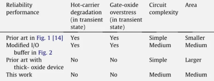
not occur in transistor MP1. The gate voltage of transistor MP1 is pulled down gradually by MN8 and the other NMOS transistors when transition from receiving 2xVDD input signal to transmitting 0-V output signal. Thus, the new proposed design does not suffer gate-oxide reliability problem in both steady state and transient state. The ability to eliminating mentioned transient reliability problem, circuit complexity and area of this work and few prior arts are briefly compared inTable 2.
4. Simulation results
4.1. Simulated waveforms for steady state operation and verification to new modifications
The simulated results of the new proposed 2xVDD-tolerant I/O buffer to prevent hot-carrier degradation and gate-oxide reliability have been verified by the HSPICE simulation in a 0.13-
l
m CMOS BSIM3 model (V3.2) with VDD of 1.2 V. The sizes for transistorsTable 2
Comparisons on reliability concerns and circuit complexity among the prior arts and this work. Reliability performance Hot-carrier degradation (in transient state) Gate-oxide overstress (in transient state) Circuit complexity Area
Prior art inFig. 1 [14] Yes Yes Simple Smaller
Modified I/O buffer inFig. 2
Yes Yes Medium Medium
Prior art with thick- oxide device
No No Simple Larger
This work No No Medium Medium
Table 1
Operations of the new proposed 2xVDD-tolerant I/O buffer in the receive/transmit states.
Operating modes Signals at I/O pad PU PD Voltage level of the floating n-well
Receive mode Low (0 V) VDD 0 VDD
Receive mode High (2xVDD) VDD 0 2xVDD
Transmit mode Low (0 V) VDD VDD VDD
Transmit mode High (VDD) 0 0 VDD
Table 3
Sizes of transistors used for the simulation in this work.
Transistors in this work Device Width (lm)/
length (lm) Transistors for main pull-up
and pull-down path
MN0, MN1, MN5 82/0.13
MP0 180/0.13
Other PMOSs and NMOSs MN3, MN4, MN6 0.68/0.13
MN8 1/0.13 MP8 0.45/0.13 MP1, MP3, MP6 4.05/0.13 MP4 36.45/0.13 MP2, MP7 8.1/0.13 MN4, MN8 2.7/0.13 MP5 0.45/0.13
Fig. 9. Simulated waveforms of the proposed mixed I/O buffer (this invention) operating at 150 MHz when receiving 2.5–0-V input signals at I/O pad.
Fig. 10. Simulated waveforms of the proposed mixed I/O buffer (this invention) operating at 150 MHz when transmitting 1.2–0-V output signals at I/O pad.
are listed inTable 3.Figs. 9and 10show the simulated waveforms of the new proposed 2xVDD-tolerant I/O buffer well operating with speed of 150 MHz in the receive mode and transmit mode, respec-tively. As shown in Fig. 9, when new proposed mixed-voltage 2xVDD I/O buffer receives 0-V and 2.5-V signal from I/O pad, it suc-cessively outputs 1.2-V and 0-V Din signal with n-well voltage
biased at 1.2 V and 2.5 V, respectively. InFig. 10, as Dout signal var-ies between 1.2 V and 0 V, new proposed I/O buffer transmits sim-ilar swing to I/O pad accordingly and n-well voltage keeps near 1.2 V.
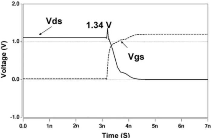
Fig. 11shows the Vdsand Vgsof MN0 in the new proposed I/O
buffer from receiving 2.5-V input signal to transmitting 0-V output signal.Fig. 12a and b shows the Vdsand Vgsof MN3 in the new
pro-posed I/O buffer from receiving 2.5-V input signal to transmitting 0-V or VDD output signal, respectively. Comparing Figs. 11 and 12a and b with previous figures (Figs. 3a and b, 4a andb, and 5a
Fig. 11. The simulated drain-to-source voltage (Vds) and gate-to-source voltage (Vgs) of MN0 in the new proposed I/O buffer during the transition from receiving 2xVDD input signal to transmitting 0-V output signal.
Fig. 12. The simulated drain-to-source voltage (Vds) and gate-to-source voltage (Vgs) of MN3 in the new proposed I/O buffer during the transition from receiving 2xVDD input signal (a) to transmitting 0-V output signal and (b) to transmitting VDD output signal.
Fig. 13. The simulated drain-to-source voltage (Vds) and gate-to-source voltage (Vgs) or source-to-gate voltage (Vsg) of transistors in the new transmitting circuits of new proposed buffer during the transition from receiving 2xVDD input signal to transmitting VDD output signal.
Table 4
Comparisons on transition times of receive/transmit operations among the prior arts and the new proposed I/O buffer with 150 MHz at 85 °C.
Mixed-voltage I/O buffer Receive mode Transmit mode Rise time (ns) Fall time (ns) Rise time (ns) Fall time (ns)
Prior art inFig. 1 [14] 0.73 0.85 0.4 0.8
Modified I/O buffer inFig. 2 0.71 0.88 0.4 1.38
This work 0.75 0.91 0.4 0.65
Fig. 14. The simulated gate-to-source (Vgs) voltage across transistor MP1 in the new proposed I/O buffer during the transition from receiving 2.5-V to transmitting 0-V output signals.
and b) correspondingly, MN0 and MN3 inFig. 1suffer serious hot-carrier degradation problem due to the larger Vds. Since the
drain-to-source voltage of MN0 and MN3 are nearly the same for the new buffer shown inFig. 8and the buffer shown inFig. 2, the capabil-ities of preventing hot-carrier degradation when receiving 2.5-V input signal are almost the same between these two buffers (Figs.
2 and 8). However, the new buffer is more efficient in area saving.
Fig. 13shows the Vdsand Vgs(or Vsg) waveforms of the
transis-tors in the transmitting circuit of the new proposed I/O buffer from receiving 2.5-V input signal to transmitting 1.2-V output signal. As shown inFig. 13, the transistors in the new proposed I/O buffer have lower drain-to-source voltage, which is more robust to pre-vent hot-carrier degradation.
Fig. 14shows the gate-to-source voltages of transistor MP1 in the new proposed I/O buffer. The peak Vsgvalue of similar PMOS
in the prior designs is larger than VDD of 1.2 V as shown inFigs.
2 and 8. However, the Vsgof MP1 in the proposed I/O buffer is close
to VDD, which is confirmed more robust than the previous designs in both hot-carrier degradation and gate-oxide reliability. Fig. 15. Current of VDD in receive mode at 85 °C for one period of 150 MHz
0-to-2xVDD swing received at I/O pad.
Fig. 16. Current of VDD in transmit mode at 85 °C for one period of 150 MHz 0-to-VDD swing transmitted at I/O pad.
Table 6
Comparisons on the root-mean-square current of receive/transmit operations among the prior arts and the new proposed I/O buffer with 150 MHz at 85 °C.
Mixed-voltage I/O buffer Receive mode (mA) Transmit mode (mA)
Prior art inFig. 1 [14] 0.88 7.56
Modified I/O buffer inFig. 2 0.95 7.29
This work 1.17 7.28
Fig. 17. (a) Layout-top-view of test chip to verify the new proposed 2xVDD-tolerant I/O buffer in a 0.13-m CMOS process. (b) Die photograph of the test chip for the new proposed I/O circuit fabricated with 0.13-m 1.2-V CMOS process.
Table 5
Comparisons on propagation delay of receive/transmit operations among the prior arts and the new proposed I/O buffer with 150 MHz at 85 °C.
Mixed-voltage I/O buffer Receive mode Transmit mode tphl (ns) tplh (ns) tp (ns) tphl (ns) tplh (ns) tp (ns) Prior art inFig. 1 [14] 0.38 0.45 0.42 0.65 0.45 0.55 Modified I/O buffer inFig. 2 0.42 0.47 0.45 1.1 0.46 0.78
4.2. Rise time, fall time and propagation delay in the new proposed I/O buffer and prior arts
The cost to maintain the driving ability is to size each main driving NMOS transistor of the prior art 2 and the new design to 1.5 times comparing with prior art 1 and size the transmission gate of the new design to 2 times of the other two prior arts. With such adjustment, the results of the rise time (tr), fall time (tf) and the propagation delay (from high to low: tphl, from low to high: tplh, and the average of tphl and tplh: tp) of the new proposed I/O buffer and the two prior arts are shown inTables 4and5. The fall time and propagation delay of the modified I/O buffer in Fig. 2 are slightly longer than the new proposed design and the prior art in
Fig. 1. The reason is attributed to the additional output loading due to MPT1 and MPT0 inFig. 2. However, effective output loading at I/O pad of prior art inFig. 1is not significantly smaller than the new proposed buffer and the modified I/O buffer inFig. 2, since the extra 10 pF capacitor at the I/O pad due to package is the dominant part in the simulation. The transition performance including rise time, fall time, and propagation delay have no obvious difference among the three circuits under proper sizing.
4.3. Power performance of the new proposed I/O and prior arts The power consumption is compared inTable 6with 0.13-
l
m CMOS model, and the root-mean-square (rms) current of the supply voltage is adopted as reference. The current of supply volt-age in one period (6.68 ns for 150 MHz) for both receive and trans-mit modes are also shown inFigs. 15and 16. According to the simulated results in transmit mode, the rms current of the supply voltage is similar among the three buffers, but the new buffer has slightly smaller value. In the receive mode, the rms power con-sumption of the new buffer is slightly larger than that of the two prior arts. The power consumption of I/O buffer in transmit mode is usually much larger than the current in receive mode because the whole buffer is required to drive large capacitance at I/O pad to deliver the swing signal. But in receive mode, besides the receiv-ing path only few nodes is charged or discharged to prevent leak-age problems, the power is mainly delivered to the core circuit from received signal at I/O pad. Thus, the new buffer has similar power performance in the receive mode.5. Experimental results
The new proposed mixed-voltage 2xVDD-tolerant I/O buffer has been fabricated in a 0.13-
l
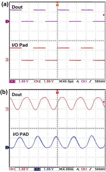
m 1.2-V CMOS process with onlythin-oxide (1.2-V) devices. The layout-top-view and the die photo-graph of test chip are shown inFig. 17a and b with the correspond-ing circuit blocks, includcorrespond-ing VDD power cell, I/O circuit, Dout pad, EN pad, Din pad, and VSS power cell.
The signals appear in the pins of fabricated chip are measured by the oscilloscope with the sampling rate of 5 GS/s and a band-width of 500 MHz.Fig. 18shows the measured waveforms of the proposed 2xVDD-tolerant I/O buffer in the receive mode to receive the 1-MHz input signals with voltage swing of 0-to-2.5 V at I/O pad, where the input data has been successfully transmitted to Din with a voltage swing of 0-to-1.2 V.Fig. 19a andbshows the measured waveforms at the I/O pad in the transmit mode to trans-mit the 10-kHz and 133-MHz output signals with a voltage swing of 0-to-1.2 V given at Dout, respectively. Some imperfectness of the measured waveforms can be attributed to the buffer size in the I/O cell, parasitic and loading effect of the PCB board. Cable line, con-nections and impedance matching of the input and output of the PCB board, oscilloscope and wave generator also cause effects such as ripples or delay.
To measure reliability performance as lifetime is not an easy task especially for circuits required tens or hundreds of years to be failure. The setup and the maintenance of the experimental condition violate the results as well. One approach to test the
Fig. 18. Measured waveforms of the proposed 2xVDD-tolerant I/O buffer operating at VDD of 1.2 V when receiving 0–2.5-V input signals at I/O pad.
Fig. 19. Measured waveforms at I/O pad of the proposed 2xVDD-tolerant I/O buffer operating at VDD of 1.2 V when transmitting 0–1.2-V output signals at (a) 10 kHz and (b) 133 MHz.
reliability of a circuit is to find out critical transistors that attribute to the reduction of the lifetime or performance. Then, simplify the reliability test to device level with specified biasing condition and apply overstress method to predict lifetime based on measured results. For the impracticality to insert pads for measuring the real voltage difference for certain transistors in the I/O buffer, the help of simulation is necessary. Since the researches on device-level reliability problem have been done by many papers as [10,16– 19], this work only provides simulated results, which are reasonable proofs to foresee that this work has better reliability performance with steady state and transient considerations. 6. Conclusion
A new 2xVDD-tolerant I/O buffer against gate-oxide overstress and hot-carrier degradation has been successfully verified in a 0.13-
l
m 1.2-V CMOS process with only thin-oxide devices. The gate-to-source, gate-to-drain, and drain-to-source voltages of the transistors in the new proposed 2xVDD-tolerant I/O buffer can be kept within the normal operating voltage (VDD) with simulated verification. The new proposed 2xVDD-tolerant I/O buffer can re-ceive 1.2-V/2.5-V input signals or transmit 1.2-V output signals up to 133 MHz, which is compatible to the I/O specifications of PCI-X in the mixed-voltage I/O interfaces.Acknowledgements
This work was partially supported by ‘‘Aim for the Top Univer-sity Plan” of the National Chiao-Tung UniverUniver-sity and Ministry of Education, Taiwan, ROC; and partially supported by National Science Council (NSC), Taiwan, under Contract of NSC 97-2220-E-009-046.
References
[1] Furukawa T, Turner D, Mittl S, Maloney M, Serafin R, Clark W, et al. Accelerated gate-oxide breakdown in mixed-voltage I/O buffers. In: Proceedings of IEEE international reliability physics symposium; 1997. p. 169–73.
[2] Singh GP, Salem RB. High-voltage-tolerant I/O buffers with low-voltage CMOS process. IEEE J Solid-State Circ 1999;34:1512–25.
[3] Chen I-C, Choi J-Y, Hu C. The effect of channel hot-carrier stressing on gate-oxide integrity in MOSFETs. IEEE Trans Electron Dev 1988;35:2253–8. [4] Liang M-S, Chang C, Yang W, Hu C, Brodersen RW. Hot-carriers induced
degradation in thin gate oxide MOSFETs. In: Technical digest of IEDM; 1983. p. 186.
[5] Renesas Technology. Semiconductor device reliability handbook, 5th ed.; 2006. [6] Hu C, Tam SC, Hsu FC, Ko PK, Chan TY, Terill KW. Hot-electron-induced MOSFET degradation – model, monitor and improvement. IEEE Trans Electron Dev 1985;32:375–85.
[7] Takeda E, Suzuki N. An empirical model for device degradation due to hot-carrier injection. IEEE Electron Dev Lett 2005;4:111–3.
[8] Koike N, Tatsuuma K. A drain avalanche hot carrier lifetime model for n- and p-channel MOSFETS. IEEE Trans Dev Mater Reliab 2004;4:457–66.
[9] Mistry K, Doyle BS. An empirical model for the left dependence of hot-carrier lifetimes of n-channel MOSFET’s. IEEE Electron Dev Lett 1989;10:500–2. [10] Chen SY, Lin JC, Chen HW, Jhou ZW, Lin HC, Chou S, et al. An investigation on
substrate current and hot carrier degradation at elevated temperatures for nMOSFETs of 0.13lm technology. In: IEEE international integrated reliability workshop final report; 2005. p. 120–2.
[11] Voldman S. ESD protection in a mixed voltage interface and multirole disconnected power grid environment in 0.5-and 0.25-lm channel length CMOS technologies. In: Proceedings of EOS/ESD symposium; 1994. p. 125 34. [12] Dabral S, Maloney T. Basic ESD and I/O design. New York: Wiley; 1998. [13] Annema A, Geelen G, Jong P. 5.5-V I/O in a 2.5-V 0.25-mm CMOS technology.
IEEE J Solid-State Circ 2001;36:528–38.
[14] Ker MD, Chen SL, Tsai CS. Overview and design of mixed-voltage I/O buffers with low-voltage thin-oxide CMOS transistors. IEEE Trans Circ Sys I 2006;53:1934–45.
[15] Serneels B, Steyaert M, Dehaene W. A 5.5 V SOPA line driver in a standard 1.2 V 0.13lm CMOS technology. In: Proceedings of IEEE European solid-state circuits conference; 2005. p. 303–6.
[16] Choi JY, Ko PK, Hu C. Hot-carrier induced MOSFET degradation under ac stress. IEEE Electron Dev Lett 1987;8:333–5.
[17] Yassine AM, Nariman HE, McBride M, Uzer M, Olasupo KR. Time dependent breakdown of ultrathin gate oxide. IEEE Trans Electron Dev 2000;47:1416–20. [18] Minami ER, Kuusinen SB, Rosenbaum E, Ko PK, Hu C. Circuit-level simulation of TDDB failure in digital CMOS circuits. IEEE Trans Semicond Manuf 1995;8:370–7.
[19] Malobabic´ S, Ellis DF, Salcedo JA, Zhou Y, Hajjar J-J, Liou J-J. Gate oxide evaluation under very fast transmission line pulse (VFTLP) CDM-type stress. In: Proceedings of the IEEE international Caribbean conference on devices, circuits and systems; 2008. p. 1–8.
[20] Park H-J, Lee K, Kim CK. A new cmos nand logic circuit for reducing hot-carrier problems. IEEE J Solid-State Circ 1996;24:1041–7.
[21] Leblebici Y. Design considerations for CMOS digital circuits with improved hot-carrier reliability. IEEE J Solid-State Circ 1996;31:1014–24.
[22] Lee T-J, Chang T-Y, Wang C-C. Mixed-voltage-tolerant I/O buffer design. In: Proceedings of the IEEE international symposium integrated circuit; 2007. p. 556–9.
[23] Bult K. Analog broadband communication circuits in pure digital deep sub-micron CMOS. In: Technical digest of IEEE international solid-state circuit conference; 1999. p. 76–7.
[24] Poon S, Atwell C, Hart C, Kolar D, Lage C, Yeargain B. A versatile 0.25 micron CMOS technology. In: Technical digest of IEDM; 1998. p. 751–4.
[25] Hargrove M, Crowder S, Nowak E, Logan R, Han LK, Ng H, et al. High-performance sub-0.08lm CMOS with dual gate oxide and 9.7 ps inverter delay. In: Technical digest of IEDM; 1998. p. 627–30.
[26] Chen S-L, Ker M-D. A new output buffer for 3.3-V PCI-X application in a 0.13-lm 1/2.5-V CMOS process. In: Proceedings of IEEE international ASIC conference advanced system integrated circuits; 2004. p. 112–55.
[27] Tsai H-W, Ker M-D. Design of 2xVDD-tolerant I/O buffer with considerations of gate-oxide reliability and hot-carrier degradation. In: Proceedings of IEEE international conference electronics, circuits and systems; 2007. p. 1240–3.
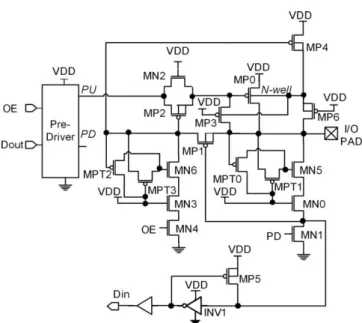
![Fig. 8. The new proposed 2xVDD-tolerant I/O buffer realized with only 1xVDD devices to prevent transistors against gate-oxide overstress and hot-carrier degradation [27] .](https://thumb-ap.123doks.com/thumbv2/9libinfo/7571552.125286/4.892.219.693.820.1105/proposed-tolerant-realized-devices-transistors-overstress-carrier-degradation.webp)