IEEE ELECTRON DEVICE LETTERS, VOL. 34, NO. 9, SEPTEMBER 2013 1157
Effects of Microwave Annealing on Nitrogenated
Amorphous In-Ga-Zn-O Thin-Film Transistor for
Low Thermal Budget Process Application
Chur-Shyang Fuh, Po-Tsun Liu, Senior Member, IEEE, Li-Feng Teng, Sih-Wei Huang, Yao-Jen Lee,
Han-Ping D. Shieh, Fellow, IEEE, and Simon M. Sze, Fellow, IEEE
Abstract— In this letter, microwave annealing technology is
proposed to reduce thermal budget for the manufacture of transparent conductive oxide thin-film transistor (TFT). With microwave annealing, a nitrogenated amorphous In-Ga-Zn-O (a-IGZO:N) TFT fabricated on glass panel behaves as a carrier mobility of 4.21 cm2/V s and threshold voltage of 2.91 V. The performance of microwave-treated a-IGZO:N TFT with annealing process duration of 300 s is well competitive with its counterpart treated by thermal furnace annealing at 350 C for 1 h. Owing to its low thermal budget and selective heating to materials of interest, the microwave annealing has great potential for flexible oxide TFT applications.
Index Terms— Flexible thin-film transistor (TFT), In-Ga-Zn-O
thin-film transistor (IGZO TFT), postannealing.
I. INTRODUCTION
I
N the recent years, amorphous indium–gallium–zinc oxide (a-IGZO) has been attracting substantial attention for the utility in thin-film transistors (TFTs) and flexible electronics because of its high mobility and light transparency [1]–[4]. In [5] and [6], the nitrogenated amorphous indium–gallium– zinc oxide (a-IGZO:N) TFT was proposed and exhibited good carrier mobility, electrical reliability, and the superior immunity against UV radiation than those of a-IGZO TFT. The sputter-deposited oxide semiconductor layer typically requires thermal annealing at∼ 400 °C for 30 min or longer to achieve a satisfactory device performance and stability [7], [8]. For flexible electronics applications, the limit of process thermal budget at flexible substrates is one of critical considerations. In this letter, a high efficient postannealing process is pro-posed using microwave technology. Among its advantages include thermal uniformity, rapid heating process, shortenedManuscript received June 19, 2013; accepted June 30, 2013. Date of publication July 19, 2013; date of current version August 21, 2013. This work was supported in part by the National Science Council of Taiwan under Contract NSC 100-2628-E-009-016-MY3. The review of this letter was arranged by Editor A. Nathan.
C.-S. Fuh and S. M. Sze are with the Department of Electronics Engineering and the Institute of Electronics, National Chiao Tung University, Hsinchu 30010, Taiwan.
P.-T. Liu, H.-P. D. Shieh and S.-W. Huang are with the Department of Photonics and Display Institute, National Chiao Tung University, Hsinchu 30010, Taiwan (e-mail: [email protected]).
L.-F. Teng is with the Department of Photonics and Institute of Electro-Optical Engineering, National Chiao Tung University, Hsinchu 30010, Taiwan. Y.-J. Lee is with the National Nano Device Laboratories, Hsinchu 30010, Taiwan.
Color versions of one or more of the figures in this letter are available online at http://ieeexplore.ieee.org.
Digital Object Identifier 10.1109/LED.2013.2272311
Fig. 1. (a) Id–Vg curves of a-IGZO TFTs and a-IGZO:N TFTs with 1P_300s microwave annealing process. The symbol of 1P_300s stands for the microwave annealed a-IGZO TFTs with microwave energy 600 W for 300 s. (b) The electrical parameters of a-IGZO TFTs and a-IGZO:N TFTs with 1P_300s microwave annealing. Inset: corresponding average value of devices in same batch.
manufacturing period, low thermal budget, and suppression of unexpected species diffusion [9], [10]. Microwave heating is also characterized by selective heating of materials, which is impossible with the typical furnace annealing process. This technology has a great potential for future flexible application and replaces the traditional thermal furnace annealing.
II. DEVICEFABRICATION
Inverted-staggered TFT devices were fabricated on a glass substrate for this research. A 100-nm-thick gate electrode of the MoW layer was initially formed by dc sputtering. A layer of 200-nm-thick silicon dioxide (SiO2) film was subsequently deposited using a
plasma-enhanced chemical vapor deposition. The active channel layer of 50-nm-thick a-IGZO were formed by a dc mag-netron sputtering with power 100 W and argon (Ar) flow rate of 10 sccm using IGZO target of In:Ga:Zn:O = 1:1:1:4 at.%. For the formation of a-IGZO:N film, the 50-nm-thick a-IGZO:N layer was deposited using reactive dc magnetron sputtering with Ar and nitrogen gas flow rates of 10 and 2 sccm, respectively. It was followed that a 100-nm-thick indium–tin oxide was then formed to act as source/drain electrodes by RF sputtering. Finally, these samples were annealed sequentially in a microwave annealing system with a microwave frequency of 5.8 GHz. The microwave power used in this letter is 600 W as denoted by 1P. The microwave annealing durations ranged from 100 to 600 s. The control sample also was fabricated separately by furnace-annealing
1158 IEEE ELECTRON DEVICE LETTERS, VOL. 34, NO. 9, SEPTEMBER 2013
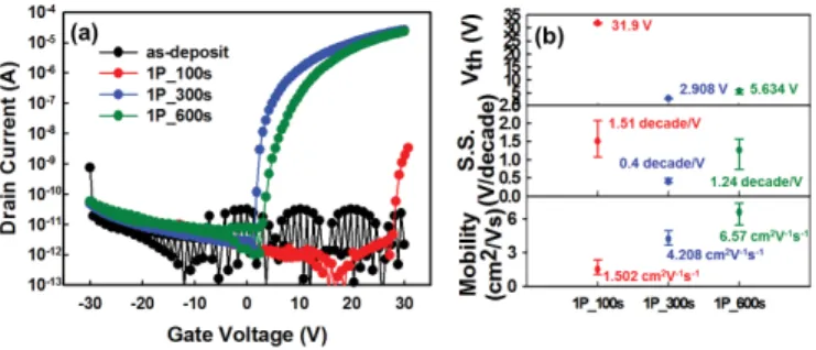
Fig. 2. (a) Id–Vg curves of a-IGZO:N TFTs with different microwave annealing processes. (b) The electrical parameters of a-IGZO TFTs correspond to each microwave annealing condition. Inset: corresponding average value of devices in same batch.
a-IGZO:N TFT at 350 °C for 1 h under nitrogen ambient for comparison with the microwave-annealed ones. Electrical measurements were measured in the dark chamber at the ambient by Keithley 4200.
III. RESULTS ANDDISCUSSION
Fig. 1(a) shows the transfer characteristics curves (Id–Vg)
of a-IGZO TFTs and a-IGZO:N TFTs with 1P microwave annealing for 300 s at a drain-to-source voltage (VDS) of
10 V. The extracted threshold voltage (Vth), mobility and
subthreshold swing (S.S.) of each device were also compared in Fig. 1(b). It is observed that the Vth of a-IGZO:N TFTs
decreased from 5.8 to 2.9 V and the mobility increased from 2.4 to 4.2 cm2/V s, compared with that of a-IGZO TFTs. It can be inferred that the microwave-treated a-IGZO:N thin film has larger carrier concentration with fermi level closer to conduction band minimum [4], [11]. Thus, the conduction electron could easily overcome the energy barrier height in the channel of device. In addition, the S.S. of microwave-treated TFT device also has a great improvement with the value 0.4 decade/V.
Fig. 2(a) shows the Id–Vgcurves of a-IGZO:N devices with
different microwave annealing conditions, and the electrical parameters were depicted as shown in Fig. 2(b). At the begin-ning, the as-deposited a-IGZO:N TFTs had large Vth and was
hardly to be turned on. As the microwave annealing duration increased from 100 to 300 s with an identical microwave power, the Vth decreased from 31.9 to 2.9 V and the
mobil-ity was enhanced from 1.5 to 4.2 cm2/Vs. The microwave annealing process enhanced the bonding of the oxygen ions with metal atoms and eliminated the defects in the channel, so that the electrical performance of device improved obviously [9], [12], [13]. The device performance was, however, degraded with excess microwave treatment. The microwave-annealed a-IGZO:N TFTs with a treatment duration of 600 s degraded slightly because of the creation of defect traps in the active layer originated from the overheating process. The trap density (Nt) could be estimated from the S.S. by the following
equation:
S.S. = loge10× kBT/e[1 + e(t Nt+ Dit)/Ci]
where t is the thickness of the a-IGZO:N active layer and Dit
is the interface trap density, assuming the trap tNt dominated
Fig. 3. Vth shift of microwave-annealed a-IGZO:N TFTs as a function of GBS durations.
Fig. 4. (a) Id–Vg curves of a-IGZO:N TFTs with different postannealing process, including microwave annealing and traditional furnace annealing. (b) Electrical parameters of a-IGZO:N TFTs correspond to each postannealing process. Inset: corresponding average value of devices in the same batch.
and Dit is negligible [14]. The Nt value of a-IGZO:N TFT
with 300 and 600 s microwave annealing was 2.48 × 10¹⁷ and 8.71 × 1017 cm−3, respectively. In addition, the phe-nomenon also existed when devices were annealed with even high microwave powers. The optimization condition for the microwave annealing is thereby critical for realistic application of a-IGZO:N TFT device.
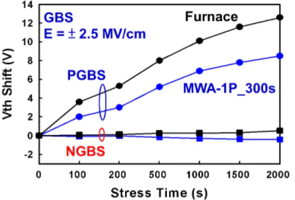
The effects of gate bias stress (GBS) on a-IGZO:N TFTs with different microwave annealing conditions are studied, as shown in Fig. 3. In GBS measurements, an electric field of 2.5 MV/cm was applied to gate electrode and source/drain electrodes were grounded. The Vth shift of
microwave-annealed a-IGZO:N TFTs after positive GBS testing decreased from the value of 14.9 V with 100 s anneal duration to a minimum of 6.8 V with 600 s anneal duration. This result suggests that the increase of microwave treatment duration could improve the electrical reliability of a-IGZO:N TFTs by eliminating the defect states in the a-IGZO:N channel layer [15].
Fig. 4(a) shows the comparison of Id–Vg curves of
a-IGZO:N TFTs annealed by microwave technology and the traditional thermal furnace. The a-IGZO:N TFTs with 1P microwave annealing for 300 s exhibited a superior perfor-mance with a lower Vth and lower S.S. than that of the
350°C furnace-annealed a-IGZO:N TFTs as shown in Fig. 4(b). The microwave-annealed a-IGZO:N TFTs performed
FUH et al.: EFFECTS OF MICROWAVE ANNEALING ON NITROGENATED a-IGZO TFT 1159
Fig. 5. Vthshift of microwave-annealed a-IGZO:N TFTs as a function of GBS durations.
even uniform electrical characteristics than that of 350 °C furnace-annealed devices. This indicated that microwave anneal technology not only provided a highly efficient process to enhance TFT device performance, but also reduced the variations in electrical characteristics between devices due to its desired features of selective heating and volumetric heating. Besides, the Nt of a-IGZO:N TFTs with microwave annealing
and furnace annealing was 2.48× 10¹⁷and 4.13× 1017cm−3, respectively. The microwave-annealed device exhibited lower trap states than that of the furnace-annealed one. After GBS test, the microwave annealed a-IGZO:N TFTs also revealed a comparable reliability with the furnace-annealed one, as shown in Fig. 5. These results were consistent with the electrical improvement in device performance of a-IGZO:N TFTs.
IV. CONCLUSION
In this letter, we have demonstrated the microwave anneal-ing technology with low thermal budget and high efficiency to enhance electrical characteristics of a-IGZO:N TFT fabricated on glass substrate. With the optimum process condition of 600 W for 300 s in this letter, electrical performance and reliability of a-IGZO:N TFTs are significantly promoted than that of the furnace-annealed one at 350 °C for 1 h because of the reduction of trap state. The proposed microwave annealing with low thermal budget would also be potential for flexible oxide TFTs application.
REFERENCES
[1] K. Nomura, H. Ohta, A. Takagi, et al., “Room-temperature fabrication of transparent flexible thin-film transistor using amorphous oxide semi-conductors,” Nature, vol. 432, no. 7016, pp. 488–492, Nov. 2004. [2] C. W. Chien, C. H. Wu, Y. T. Tsai, et al., “High-performance flexible
a-IGZO TFTs adopting stacked electrodes and transparent polyimide-based nanocomposite substrates,” IEEE Trans. Electron Devices, vol. 58, no. 5, pp. 1440–1446, May 2011.
[3] Y. H. Yang, S. S. Yang, C. Y. Kao, et al., “Chemical and electrical properties of low-temperature solution-processed In-Ga-Zn-O thin-film transistors,” IEEE Electron Device Lett., vol. 31, no. 4, pp. 329–331, Apr. 2010.
[4] N. Münzenrieder, K. H. Cherenack, and G. Tröster, “The effects of mechanical bending and illumination,” IEEE Electron Device Lett., vol. 58, no. 7, pp. 2041–2048, Jul. 2011.
[5] P. T. Liu, Y. T. Chou, L. F. Teng, et al., “Ambient stability enhancement of thin-film transistor with InGaZnO capped with InGaZnO:N bilayer stack channel layers,” IEEE Electron Device Lett., vol. 32, no. 10, pp. 1397–1399, Oct. 2011.
[6] P. T. Liu, Y. T. Chou, L. F. Teng, et al., “Nitrogenated amorphous InGaZnO thin film transistor,” Appl. Phys. Lett., vol. 98, no. 5, pp. 052102-1–052102-3, Jan. 2011.
[7] K. Nomura, T. Kamiya, Y. Kikuchi, et al., “Comprehensive studies on the stabilities of a-In-Ga-Zn-O based thin film transistor by constant current stress,” Thin Solid Films, vol. 518, no. 11, pp. 3012–3016, Mar. 2010.
[8] C. S. Fuh, S. M. Sze, P. T. Liu, et al., “Role of environmental and annealing conditions on the passivation-free In-Ga-Zn-O TFT,” Thin Solid Films, vol. 520, no. 5, pp. 1489–1494, Dec. 2011.
[9] L. F. Teng, P. T. Liu, Y. J. Lo, et al., “Effects of microwave annealing on electrical enhancement of amorphous oxide semiconductor thin film transistor,” Appl. Phys. Lett., vol. 101, no. 13, pp. 132901-1–132901-4, Sep. 2012.
[10] J. R. Groza, S. H. Risbud, and K. Yamazaki, “Plasma activated sintering of additive-free AlN powders to near-theoretical density in 5 minutes,” J. Mater. Res., vol. 7, no. 10, pp. 2643–2645, Jan. 2011.
[11] K. Reyes-Gil, E. Reyes-García, and D. Raftery, “Nitrogen-doped In2O3 thin film electrodes for photocatalytic water splitting,” J. Phys. Chem. C, vol. 111, no. 39, pp. 14579–14588, Sep. 2007.
[12] X. Huang, C. Wu, H. Lu, et al., “Enhanced bias stress stabil-ity of a-InGaZnO thin film transistors by inserting an ultra-thin interfacial InGaZnO:N layer,” Appl. Phys. Lett., vol. 102, no. 19, pp. 193505-1–193505-4, May 2013.
[13] C. E. Kim, E. N. Cho, P. Moon, et al., “Density-of-states modeling of solution-processed InGaZnO thin-film transistors,” IEEE Electron Device Lett., vol. 31, no. 10, pp. 1131–1133, Oct. 2010.
[14] K. Nomura, T. Kamiya, H. Ohta, et al., “Defect passiva-tion and homogenizapassiva-tion of amorphous oxide thin-film transis-tor by wet O2 annealing,” Appl. Phys. Lett., vol. 93, no. 19, pp. 192107-1–192107-3, Nov. 2008.
[15] K. Hoshino, D. Hong, H. Q. Chiang, et al., “Constant-voltage-bias stress testing of a-IGZO thin-film transistors,” IEEE Trans. Electron Devices, vol. 56, no. 7, pp. 1365–1370, Jul. 2009.