good agreement between the measurement and simulation is ob-tained. Some little discrepancy between the simulated and mea-sured results can be attributed to the manufacture error as well as the inaccuracy of the antenna model implemented in the simula-tion. The measured impedance bandwidth, which is determined from 2:1 VSWR or about 10 dB return loss, reaches 8 GHz (3–11 GHz), which covers the operating bandwidth of the UWB com-munication (3.1–10.6 GHz).
The simulated and measured radiation patterns at 4, 6, and 8 GHz for the structure for which Vivaldi 1 is the active element are given in Figures 3–5, respectively. The E-plane of this antenna is x–y plane and the H-plane is x–z plane. The measured results in azimuth plane agree well with the simulation and show good radiation pattern with half-power beamwidth (HPBW) as broad as 90° over the entire band. That is, the antenna composed of four direction parts can cover all the 360° of the horizontal plane. The directivity of the antenna is about 6 dB. The front to back ratio reaches more than 10 dB. The radiation pattern is isotropic in the azimuth plane for the symmetrical structure of the antenna, thus high front to back ratio sector beam can be obtained in the other three directions through changing the status of the switches. 4. CONCLUSION
The sector beam planar Vivaldi array antenna operating in the 3.1–10.6 GHz for UWB application has been proposed and imple-mented. The antenna shows good impedance matching in a wide bandwidth of 8 GHz and good radiation pattern with HPBW as
broad as 90° and high front to back ratio of more than 10 dB over the entire band. Desired sector beam in four directions of the azimuth plane can be achieved by adjusting on/off state of the switches. That is, the isotropic radiation pattern can be obtained for the symmetrical structure of the antenna.
ACKNOWLEDGMENT
This work was supported by Qualcomm. Their support is grate-fully acknowledged.
REFERENCES
1. P.F. Wahid, M.A. All, and B.C. DeLoach, A reconfigurable Yagi antenna for wireless communications, Microwave Opt Technol Lett 38 (2003), 140 –141.
2. H.R. Chuang and L.C. Kuo, 3-D FDTD design analysis of a 2.4 GHz polarization-diversity printed dipole antenna with integrated balun and polarization-switching circuit for WLAN and wireless communication applications, IEEE Trans Microwave Theory Tech 51 (2003), 374 –381. 3. A. Abbaspour-Tamijani and K. Sarabandi, An affordable millimeter-wave beam-steerable antenna using interleaved planar subarrays, IEEE Trans Antennas Propagat 51 (2003), 2193–2202.
4. N. Li, W.H. Chen, and Z.H. Feng, A switched sector beam planar antenna, IEEE Antennas Propagat Soc Int Symp Dig 1A (2005), 230 – 233.
5. C.S. Deluccia, D.H. Werner, P.L. Werner, M. Fernandez Pantoja, and A. R. Bretones, A novel frequency agile beam scanning reconfigurable antenna, IEEE Antennas Propagat Soc Int Symp Dig 2 (2004), 1839 – 1842.
6. F.L. Chen, W.H. Chen, L. Yang, and Z.H. Feng, A novel switched-sector planar antenna using parasitic elements, IEEE Antennas Propagat Soc Int Symp Dig 1 (2004), 855– 857.
7. C.Y. Huang and W.C. Hsia, Planar elliptical antenna for ultra-wideband communications, Electron Lett 41 (2005), 296 –297.
8. J. Liang, C.C. Chiau, X. Chen, and C.G. Parini, Study of a printed circular disc monopole antenna for UWB systems, IEEE Trans Anten-nas Propagat 53 (2005), 3500 –3504.
© 2007 Wiley Periodicals, Inc.
Ka-BAND 0.18
m CMOS LOW NOISE
AMPLIFIER WITH 5.2 dB NOISE
FIGURE
Win-Ming Chang, Zi-Hao Hsiung, and Christina F. Jou Department of Communication Engineering, National Chiao Tung University, Hsinchu, Taiwan
Received 24 September 2006
ABSTRACT: A Ka-band low noise amplifier (LNA) using three
cas-caded stages was designed and implemented in a standard 0.18m CMOS technology. The fabricated Ka-band LNA achieves power gain (S21) above 12 dB from 30 to 32 GHz and a minimal noise figure of 5.2 dB at 31.5 GHz. The three cascaded stages LNA consume 15.58 mA from 1 V power supply. Compared with the recent published literatures, this LNA operates at the highest frequency ever reported by standard bulk 0.18m CMOS process. © 2007 Wiley Periodicals, Inc.
Microwave Opt Technol Lett 49: 1187–1189, 2007; Published online in Wiley InterScience (www.interscience.wiley.com). DOI 10.1002/mop. 22383
Key words: Ka-band; LNA; CMOS 1. INTRODUCTION
As the growing demand for wider bandwidth and higher commu-nicated data rates, integrated circuits moving toward higher fre-Figure 5 Measured E-plane and H-plane patterns at 8 GHz
quencies have gotten more and more attention. In the past, most of the millimeter wave applications are occupied by GaAs-based HEMT and HBT technology due to lossless substrate. However, the rapid development of CMOS devices and several published works show that implementing a Ka-band low noise amplifier (LNA) by standard CMOS technology is accomplishable [1– 4]. Since the transistor gain is not plentiful at such high frequencies, multistage-cascaded structures are generally used to perform high gain and low noise. This article reports the Ka-band CMOS LNA implemented in a standard bulk 0.18m CMOS technology and well-performed noise figures were achieved in this work. 2. CIRCUIT DESIGN
The standard 0.18m CMOS transistors have been demonstrated with sufficient unit-gain frequency (fT) and maximum oscillation frequency (fmax) [2, 3]. Since there is no gain while operating at millimeter wave range, three-stage cascaded structure is designed to achieve the gain requirement for this Ka-band LNA.
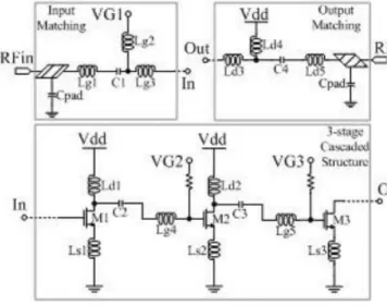
Figure 1 shows the LNA schematic. The first stage is designed for low noise, and its gain depresses the noise contributing from following two stages. The second and third stages are designed to perform higher gain at 30 GHz. The source degeneration inductor, Ls1, is used for stability issue and the matching to the real part of input impedance to 50⍀. Furthermore, the source impedance for maximum power transfer and minimum noise figure move closer by adding Ls1. The input matching network is constructed sequen-tially by moving 50⍀ to the selected ⌫sand the pad influence is also considered. To have a compact size and lower noise figure, the dc bias and blocking capacitor are also absorbed into the designed input matching network. For interstage matching consideration, Lg4 is the input matching network for M2 while Ld1 and C2 form the L-shaped structures with high-pass characteristic for the output matching network of M1 (Fig. 1). The interstage matching net-works execute conjugate matching between the drain of M1 and the gate of M2. The same interstage matching scheme is also completed between M2 and M3. Finally, the output matching network of M3 is similar to the input matching network of M1. 3. LAYOUT CONSIDERATION
Figure 2 shows the micrographic of the Ka-band LNA. In such high frequency, each transmission lines as well as inductors should be taken into consideration for matching network and they are
implemented on the top metal layer of 2-m-thick AlCu for lower resistive loss. Several additional transmission lines are added in the LNA topology for the purpose of reducing the unwanted coupling effects. The inductors are separated with at least 50m [3]. To stabilize the supply voltage and filter out the supply noise, large numbers of bypass capacitors are connected in parallel between each power supply and ground.
4. MEASUREMENT RESULTS
All the measurements are performed on wafer. Figure 3 shows the measured small signal gain and noise figure from 25 to 40 GHz. The measured results reveal that a power gain above 12 dB is achieved from 30 to 32 GHz and 3 dB bandwidth of 7 GHz from 28 to 35 GHz. The measured minimum noise figure of 5.2 dB at 31.5 GHz has been presented in this Ka-band CMOS LNA with 15.58 mA from 1 V power supply. The measured input and output Figure 1 Topology of the Ka-band LNA
Figure 2 Microphotographic of Ka-band LNA (0.68 mm⫻ 0.74 mm). [Color figure can be viewed in the online issue, which is available at www.interscience.wiley.com]
Figure 3 Gain and noise figure performance
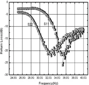
return losses are shown in Figure 4. Above 20 dB return losses are accomplished for input at 32 GHz and output at 35 GHz. However, the input and output return losses at 32 GHz are 6.3 and 20.67 dB, respectively. An input third-order intercepted point (IIP3) of⫹0.9 dB m is also measured and high linearity is attained from 1 V power supply. This Ka-band LNA has demonstrated that standard bulk 0.18m CMOS LNA can achieve high gain and low noise with reasonable power consumption above 30 GHz. Table 1 com-pares our measurement results with recent published literatures of standard bulk CMOS LNAs above 20 GHz [1– 4].
5. CONCLUSION
This article presents a Ka-band LNA using three cascaded stages in a standard 0.18m CMOS technology. A power gain (S21) of above 12 dB from 30 to 32 GHz and a minimal noise figure of 5.2 dB at 31.5 GHz while consuming 15.58 mA from 1 V power supply have demonstrated in this Ka-band LNA. Compared with the recent published literatures operating above 20 GHz by using standard bulk 0.18m CMOS process, this LNA operates at the highest frequency ever reported.
ACKNOWLEDGMENTS
The authors thank the Chip Implementation Center (CIC) of the National Science Council, Taiwan, Republic of China, for support-ing the TSMC CMOS process. And the measurement results are also accomplished in CIC.
REFERENCES
1. G. Xiang and A. Hajimiri, A 24-GHz CMOS front-end, Solid State Circuits, IEEE Journal of 39 (2004), 368 –373.
2. K.-W. Yu, Y.-L. Lu, D.-C. Chang, V. Liang, and M.F. Chang, K-band low-noise amplifiers using 0.18 /spl mu/m CMOS technology, Micro-wave Wireless Components Lett 14 (2004), 106 –108 [see also IEEE Microwave and Guided Wave Letters].
3. S.-C. Shin, M.-D. Tsai, R.-C. Liu, K.-Y. Lin, and H. Wang, A 24-GHz 3.9-dB NF low-noise amplifier using 0.18 /spl mu/m CMOS technol-ogy, Microwave Wireless Components Lett 15 (2005), 448 – 450 [see also IEEE Microwave and Guided Wave Letters].
4. M.A. Masud, H. Zirath, M. Ferndahl, and H.-O. Vickes, 90 nm CMOS MMIC amplifier, In Radio Frequency Integrated Circuits (RFIC) Sym-posium, Digest of Papers IEEE, 2004, 201–204.
5. D. Linten, L. Aspemyr, W. Jeamsaksiri, J. Ramos, A. Mercha, S. Jenei, S. Thijs, R. Garcia, H. Jacobsson, P. Wambacq, S. Donnay, and S. Decoutere, Low-power 5 GHz LNA and VCO in 90 nm RF CMOS, In VLSI Circuits Symposium, Digest of Technical Papers, 2004, 372–375. © 2007 Wiley Periodicals, Inc.
DESIGN APPROACH FOR REALIZING
TWO-DIMENSIONAL
ELECTROMAGNETIC BAND GAP
STRUCTURES
George S. A. Shaker and Safieddin Safavi-Naeini
Department of Electrical and Computer Engineering, University of Waterloo, Waterloo, ON, Canada, N2L 3G1
Received 24 September 2006
ABSTRACT: This paper presents a simple approach for designing
two-dimensional electromagnetic band gap structures (EBGs). The approach is based on designing a planar band pass filter at a desired center fre-quency. A simple modification is introduced to the well known design steps of the filter. This modification allows for specifying the high impedance property of the structure, as well as its stop band, using a circuit simulator. © 2007 Wiley Periodicals, Inc. Microwave Opt
Technol Lett 49: 1189 –1192, 2007; Published online in Wiley Inter-Science (www.interscience.wiley.com). DOI 10.1002/mop.22382 Key words: electromagnetic band gaps; artificial magnetic conductors;
high impedance surfaces; metamaterials; antennas
1. INTRODUCTION
Recently, interest has increased significantly in electromagnetic band gap structures, widely known as EBGs [1–5]. EBGs emerged as structures which possess two unique properties simultaneously. The first is a band stop characteristic, which means that the flow of electromagnetic waves in a tangential direction to the EBG surface (surface waves) is prohibited. The second is a high impedance Figure 4 Input and output return loss
TABLE 1 Comparison with Published CMOS LNAs Operating Above 20 GHz
This Work Ref. 1 Ref. 2 Ref. 3 Ref. 4
Process CMOS (0.18m) CMOS (0.18m) CMOS (0.18m) CMOS (0.18m) CMOS (90 nm)
fRF(GHz) 32 21.8 23.7 24 20 Vdd(V) 1 1.5 1.8 1 1.5 S21 (dB) 12.08 15 12.86 13.1 5.8 S11/S22 (dB) ⫺6.3/⫺20.67 ⫺/⫺ ⫺11/⫺22 ⫺15/⫺20 ⫺20 Pc(mW) 15.58 24 54 14 10 NF (dB) 5.224 6 5.6 3.9 6.4
IIP3 (dBm) 0.9 N/A 2.04 0.54 N/A