國
立
交
通
大
學
電子工程學系 電子研究所
博 士 論 文
高敏感度之矽鍺奈米生醫感測之研究與應用
The Investigation and Application of High Sensitivity SiGe Nanowire for
Bio-sensor
研 究 生:郭俊銘
指導教授:張國明 教授
高敏感度之矽鍺奈米生醫感測之研究與應用
The Investigation and Application of High Sensitivity SiGe Nanowire for
Bio-sensor
研 究 生:郭俊銘 Student:Jiun-Ming Kuo
指導教授:張國明 Advisor:Kow-Ming Chang
國 立 交 通 大 學
電子工程學系 電子研究所
博 士 論 文
A DissertationSubmitted to Department of Electronics Engineering and Institute of Electronics
College of Electrical and Computer Engineering National Chiao Tung University
in partial Fulfillment of the Requirements for the Degree of
Doctor of Philosophy in
Electronics Engineering
July 2008
Hsinchu, Taiwan, Republic of China
高敏感度之矽鍺奈米生醫感測之研究與應用
學生:郭俊銘 指導教授:張國明 博士
國立交通大學
電子工程系電子研究所
中文摘要
在這篇論文中我們探討矽鍺奈米線的感測能力之優缺點,並針對氧化過後 之矽鍺薄膜做研究,緊接著將此結果應用於矽鍺奈米線並作感測能力之探論。 首先,先探討著矽鍺奈米線與傳統的多晶矽奈米線差異,矽鍺奈米線擁有 優於傳統多晶矽奈米線較高的導通電流,但也擁有著較高的接觸電阻。 接著,我們利用傳統的薄膜電晶體元件做為我們測試結構,探討著不統的 氧化條件下所造成的電流增益情況。越高的溫度及越長的時間氧化,都會造成其 電流增益。此外,我們嘗試著在不同的氧化溫度與時間的條件已達到相同的氧化 厚度,其電流增益也相同,此結果為相同的氧化厚度所導致的鍺析出也是一樣的。 其次,我們探討著不同的矽鍺濃度的奈米線的蛋白質感測。越高的鍺濃度 擁有較高的感測能力,但是太高的鍺濃度其感測能力卻下降,我們推測是因為表 面擁有過多的缺陷所導致。 再者,我們探討著矽鍺奈米線氧化厚的感測能力,在低濃度時,其感測能 力隨著氧化溫度升高而提高,但是隨著濃度的提高其感測能力可能會因為過高的 氧化溫度而下降,其原因可能為氧化溫度或時間過久使的鍺濃度超過一定值時會 造表面缺陷上升。 最後,除了從材料或表面處理外,我們提出了一個新穎的結構來提升其奈 米線的敏感度,利用雙層的高導通與低導通電特性,來有效的決定電流的路徑,The Investigation and Application of High Sensitivity SiGe
Nanowire for Bio-sensor
Student: Jiun-Ming Kuo Advisors: Dr. Kow-Ming Chang
Department of Electronics Engineering &
Institude of Electronics
National Chiao-Tung University
Hsinchu, Taiwan, R.O.C
Abstract
In this thesis, we concentrate our efforts on the advantage and disadvantage of SiGe nanowire and Poly-Si nanowire for bio-sensor. The behavior of oxidation for SiGe film was studied in the follows. The application of the SiGe oxidation was used to enhance the sensitivity in the end of thesis.
First, we demonstrated the electric properties of SiGe and Poly-Si nanowires. The higher drive current is obtained for SiGe nanowire, but the disadvantage of the higher contact resistance appeared for SiGe nanowire.
Secondly, the thin-film-transistor (TFT) was used to understand the increase of drive current after different oxidation conditions. The higher drive current obtained for the higher temperature, oxidation time and oxygen flow. Besides, the same oxide thicknesses were achieved by controlling the different oxidation time and temperature.
The same drive current improves for the same oxide thickness. The reason come form the same Ge condensed after oxidation.
Third, we studied the sensitivity of SiGe nanowire with different Ge concentration. The higher sensitivity was observed for the SiGe nanowire with high Ge concentration. However, the sensitivity decreased for the over-high Ge concentration. The reason may be that the higher defect appears on the surface.
Finally, we used the Ge condensation technique on the SiGe nanowire for bio-sensor. The sensitivity improved for the SiGe nanowire with low Ge concentration after high temperature oxidation. However, the sensitivity decreased for SiGe nanowire with higher Ge concentration. It may be that the higher defect appears on the surface.
In the end of the thesis, we introduce a novel structure to improvement the sensitivity. A double layer with high/low drive current is combined to achieve this point. The sensitivity improves under the same electric filed change by controlling the current through.
誌
謝
本論文的完成首先要感謝我的指導老師張國明教授,張教授在研究上的指 導確切詳盡,在生活上的關心無微不至,讓我這五年的博士生活中受益良多,其 幫忙與建議,讓我的論文發表更順利。 在完成論文的建立過程中,還要特別感謝實驗室的學長學弟們的幫助:游 凱翔學長、楊文誌學長、王敬業學長、朱俊宜學長、趙高毅學長、吳資麟學弟、 曾文賢學弟、吳恆信學弟、梁家榮學弟、趙文全學弟、滕聚翔學弟、王育彬學弟、 鄭文魁學弟在實驗上的建議與幫忙; 林建宏學弟、陳伯寧學弟和黃士軒學弟等在 我心情低落時陪我放鬆心情;感謝交通大學奈米中心(NCTU-NFC)林素珠小姐、 徐秀鑾小姐、何惟美小姐在實驗上的幫忙。 最後謹以此論文現給我的父母親郭春坤先生與陳寶春女士,感謝他們在我 求學階段的鼓勵與支持,感謝我的哥哥和妹妹們的鼓勵,因為你們的存在,我才 能順利完成我的博士論文,謝謝你們。
Contents
Chinese Abstract………...i
English Abstract……….iii
Acknowledgment……….v
Contents………..vi
Table Captions……….……….. x
Figure Captions………...xi
Chapter 1
Introduction of Nanowires
1.1 The Application of Nanowires……….…………...1
1.2 The Materials of Nanowires Sensor………5
1.3 Motivation
………...………8
Chapter 2
Fabrication of Nanowires
2.1 Introduction………..……….………....10
2.1.1 Lithography with Photons…………..………10
2.1.2 Machining Using AFM, STM, NSOM.…………...10
2.1.3 Nanoimprint Lithography (NIL)...………..…………11
2.1.4 Spacer Formation……....………12
2.1.5 Vapor State Synthesis….…….………12
2.1.6 Vapor-Liquid-Solid (VLS) Growth Approach...…….13
2.1.7 Electrochemical Deposition…..……..………13
2.2 Experiment………..………...15
2.3 The Dimension of Nanowires.………...…………...18
2.4 Results and Discussions...……….………...19
2.5 Summary ……….………...25
Chapter 3 Electrical Properties of SiGe Film with Various
Oxidation Conditions
3.1.1 An Overview of the Applications of High Mobility
SiGe Alloy………27
3.1.2 Ge Condensation Process in SiGe Film………..27
3.1.3 Mechanism of SiGe Oxidation………28
3.1.4 Oxidation Behavior of SiGe……..………29
3.1.1 Motivation………27
3.2 The Process Flow of SiGe-Based P-MOSFET….……....32
3.3 Results and Discussions………..…………....37
3.3.1 Influence of Oxidation Temperature on Electrical
Properties………37
3.3.2 Influence of Oxidation Time on Electrical
Properties………38
3 . 3 . 3 I n f l u e n c e o f O x y g e n f l o w o n E l e c t r i c a l
Properties………40
3.3.4 Influence of the Thickness of Pre-oxide on Electrical
Properties………41
3.3.5 Influence of Oxidation Rate on Electrical
Properties………….………43
3.3.6 Influence of Annealing after Oxidation on Electrical
Properties………37
3.4 Summary………..……….………....32
Chapter 4 The Higher Current of SiGe Nanowire by Oxidation
4.1 Introduction………..47
4.2 Experiment………48
4.3 Results and Discussions………...51
4.4 Summary………...53
Chapter 5 The Ge enhances the Sensitivity for Bio-Sensor
5.1 Introduction………..………..54
5.2 Experiment……….………..………..………55
5.3 The Dimension of nanowires………59
5.4 Results and Discussions………...60
5.5 Summary………...68
Chapter 6 The Improvement of the Sensitivity for Bio-Sensor by
SiGe Nanowire Oxidation
6.1 Introduction………..69
6.2 Experiment………70
6.3 Results and Discussions………...73
6.4 Summary………...84
7.1 Conclusions………..85
7.2 Feature Works………86
References………..………88
Vita………..…95
T
ABLE
C
APTIONS
Table 1-1 The applications of various materials of nanowire sensor...8
Table 3.1 Influence of Oxidation Temperature Experiment…………36
Table 3.2 Influence of Oxidation Time Experiment………36
Table 3.3 Influence of Oxygen Flow Experiment………36
Table 3.4 Influence of Thickness of Pre-Oxide Experiment…………36
Table 3.5 Influence of Oxidation Rate Experiment……….36
Table 3.6 Influence of Annealing after Oxidation Experiment……..36
F
IGURE
C
APTIONS
CHAPTER 1
Figure 1.1 (a) The diagram of silicon nanowire. (b) The conductance changed with back side gate voltage changed…………..………...2 Figure 1.2 (a) The mechanism of pH solution detection. (b) The conductance
changed with different pH buffer solutions……….3 Figure 1.3 (a) Schematic illustrating a biotin-modiÞed SiNW (left) and subsequent binding of streptavidin to the SiNW surface (right). (b) The conductance increases by positive biotin adsorption. However, the chemical link is irreversible. (c) The unchanged-conductance is found because of unmodified……….4
Figure 1.4 (a) The conductance does not change by un-match DNA (b) The
conductance enhanced after matched-DNA modified…………5 Figure 1.5 Response of the SnO2 nanobelts to CO at a working temperature of 400
°C and 30% RH………..……….……….6 Figure 1.6 Measured time-dependent current through an individual CPNW sensor
upon exposure to NH3 gas. The nanowire device being tested was
about 335 nm in diameter……….………7 Figure 1.7 Sensor resistance responses for hydrogen concentration varied in a range from 0.2 to 1% by pulses……….………8 Figure 1.8 Drain current of N- and P-MOSFETs are improved with
CHAPTER 2
Figure 2.1 Schema of Scanning Probe Lithography (SPL)……….11
Figure 2.2 Schema of imprint process. ……….……… 12
Figure 2.3 Schema of spacer process………..12
Figure 2.4 Mechanism of spacer process……….13
Figure 2.5 The mechanisms of the laser ablation formation technique…………14
Figure 2.6 3000Å SiO2 layer was grown on Si substrate………16
Figure 2.7 Definition of the active area. The height of oxide step is 1000Å…….16
.Figure 2.8 150Å Amorphous Si layer is deposited on SiO2 layer……….17
Figure 2.9 SiGe films with different Ge concentration were deposited on α-Si layer………..17
Figure 2.10 The definition of the S/D region and nanowire. (a) The 3-D view (b) The top view……….17
Figure 2.11 Remove one side of the parallel SiGe spacer to cut off the leakage current (a) The 3-D view (b) The top view………18
Figure 2.12 Defined Al contact pad. (a) The 3-D view (b) The top view………...18
Figure 2.13 (a) The top view of poly-Si nanowire. (b) The cross-section view of poly-Si nanowire with 174 nm in height (H) and 76.9 nm in width (W). (c) The Si0.93Ge0.07 nanowire with H = 280 nm and W = 108 nm. (d) The Si0.89Ge011 nanowire with H = 86 nm and W = 44 nm ……….19 Figure 2.14 (a) The leakage current of the isolated pad without nanowire. The
current is about 2 pA. (b) The diagram for leakage current test structure. (c) The drive current of Poly-Si nanowire with 15 um in length. (d) The current of Si0.93Ge0.07 nanowire with 15 um in length. (e) The current of Si0.89Ge0.11 nanowire with 15 um in length. (f) The normalized current of Poly-Si and SiGe nanowires. The higher drive
current is obtained by SiGe nanowire with higher Ge concentration.. 21 Figure 2.15 (a) and (b) shows the drive current of Si0.89Ge0.11 and Poly-Si
nanowire with 5 um in length after S/D implant. (c) The normalized current of Poly-Si and Si0.89Ge0.11 nanowires after Source/Drain implanted. The insert picture is the diagram of nanowire with PR covered. (d) and (e) shows the drive current of Si0.89Ge0.11 and Poly-Si nanowire with 15 um in length after S/D and channel implant. (e) The normalized current of Poly-Si and Si0.89Ge0.11 nanowires after Source/Drain and channel implanted. The insert is the diagram of nanowire without PR covered………23 Figure 2.16 (a) and (b) show the resistance V.S. the contact pads of Poly-Si/Al. (c)
and (d) show the resistance v.s. the contact pads of Si0.89Ge0.11/Al. The intersection of the y-axial and fitted line is the contact resistance between the aluminum and Poly-Si/SiGe pad………25
CHAPTER 3
Figure 3.1 Scanning TEM image and Ge profile across the layers Obtained by EDS measurement………..…………..30 Figure 3.02 The Ge fractions after dry oxidation………31 Figure 3.3 Plane-view TEM observations (a) before and (b) after oxidation at the temperature of 1200 °C………31 Figure 3.4 (a) The stack of SiGe/SiO2/Si. (b) Top view of SiGe-S/D and channel pattern. (c) The PE gate oxide and Poly gate were deposited. (d) Poly gate pattern……….. …33 Figure 3.5 The cross-section view of p-type SiGe-thin-film-transistor………..35
Figure 3.6 (a) Id-Vg characteristics of different oxidation temperatures. (b) Id-Vd characteristics………...38 Figure 3.7 (a) Id-Vg characteristics after different oxidation times; the
temperature is 1000℃ (b) Id-Vd characteristics……….…39 Figure 3.8 (a) Id-Vg characteristics after different oxygen flow rates at 1000℃ (b)
Id-Vd characteristics……….41 Figure 3.9 a) Id-Vg characteristics with different thicknesses of pr-oxide
deposited before oxidation ; the temperature is 1000℃ and the time is 36 min. (b) Id-Vd characteristics………..42 Figure 3.10 (a) Id-Vg characteristics of different oxidation rates. (b) Id-Vd
characteristics………...43 Figure 3.11 (a) Id-Vg characteristics of annealing applied. (b) Id-Vd
characteristics………...…44
CHAPTER 4
Figure 4.1 3000Å SiO2 layer was grown on Si substrate………49 Figure 4.2 Definition of the active area. The height of oxide step is 1000Å…….49
Figure 4.3 150Å Amorphous Si layer is deposited on SiO2 layer……….50
Figure 4.4 SiGe films with different Ge concentration were deposited on α-Si layer………..……….50 Figure 4.5 The definition of the S/D region and nanowire. (a) The 3-D view (b) The top view………...………..…50 Figure 4.6 Remove one side of the parallel SiGe spacer to cut off the leakage current (a) The 3-D view (b) The top view……….51 Figure 4.7 Defined Al contact pad. (a) The 3-D view (b) The top view……..….51 Figure 4.8 (a) The cross-section view of Si0.93Ge0.07 nanowire with 192 nm in
height and 77.7 nm in width. (b) the SEM image of SiGe nanowire with 168 nm in height and 55.9 nm in width after 2 min. 900 ℃ oxidation and (c) shows that with 160 nm in height and 42.8 nm in
width after 2 min. 950 oxidation℃ ………..51
Figure 4.9 (a) ID-VD curve of Si0.93Ge0.07 nanowire with unoxidized, 900 ℃ 2 min. and 950 ℃ 2 min. respectively. (b) The conductivity of Si0.93Ge0.07 nanowire with unoxidized, 900 ℃ 2 min. and 950 ℃ 2 min. respectively………..…………...….53
CHAPTER5
Figure 5.1 Drain current of N- and P-MOSFETs are improved with Si/SiGe-channel………55 Figure 5.2 3000Å SiO2 layer was grown on Si substrate………57 Figure 5.3 Definition of the active area. The height of oxide step is 1000Å…….57
Figure 5.4 150Å Amorphous Si layer is deposited on SiO2 layer…….….57
Figure 5.5 SiGe films with different Ge concentration were deposited on α-Si layer……….………...58 Figure 5.6 The definition of the S/D region and nanowire. (a) The 3-D view (b) The top view……….58 Figure 5.7 Remove one side of the parallel SiGe spacer to cut off the leakage current (a) The 3-D view (b) The top view………..58 Figure 5.8 Defined Al contact pad. (a) The 3-D view (b) The top view…….…..59 Figure 5.9 (a) The cross-section view of Si0.93Ge0.07 nanowire with 192 nm in height (H) and 77.7 nm in width (W). (b) The Si0.89Ge0.11 nanowire with H = 184 nm and W = 45.4 nm (c) The Si0.8Ge0.2 nanowire with H = 159 nm and W = 65.9 nm. (d) The Si0.7Ge0.3
nanowire with H = 153 nm and W = 54.5 nm. (e) The Si0.6Ge0.4 nanowire with H = 172nm and W = 53.4 nm………60 Figure 5.10 (a) The ID-VD curve of Si0.93Ge0.07 nanowire. (b) The cut-off current between the two contact pads……….61 Fig. 5.11 (a) The mechanism image of the 3-amino-propyl-trime-thoxy-silane APTS and bis-sulfo-succinimidyl suberate BS3 molecular linkage on the nanowire. (b) The conductance of N-type Si0.93Ge0.07 nanowire with/without APTS and BS3 modified. The conductance increases for positive charge of APTS and decreases for the negative charge of BS3………63 Figure 5.12 (a) The conductance of N-type Si0.89Ge0.11 nanowire with/without
APTS and BS3 modified. The conductance increases for positive charge of APTS and decreases for the negative charge of BS3. (b) (c) (d) shows the conductance of N-type Si0.8Ge0.2, Si0.7Ge0.3 and Si0.6Ge0.4 SiGe nanowire respectively……….. …64 Figure 5.13 (a) The percentage of the variation in conductance of SiGe nanowire with different Ge concentrations after APTS modified. (b) The percentage of the variation in conductance of SiGe nanowire with different Ge concentrations after BS3 connected to it………66 Figure 5.14 (a) The conductance of Si0.93Ge0.07 nanowire after IgG connected to it. (b) The percentage of the variation in conductance of SiGe nanowire with different Ge concentrations after IgG connected to it………….67
CHAPTER 6
Figure6.1 (a) SiGe/SiO2/Si stack. For the step of oxide, the height of different SiGe is formed on the plane film and spacer place. (b) The Spacer
SiGe nanowire and the huge block (for the contact) were remained after Dry etching. (c) The SiGe nanowires were isolated. (d) The cross-section view of Si0.93Ge0.07 nanowire with 192 nm in height and 77.7 nm in width………72 Figure 6.2 (a) The mechanism image of the 3-amino-propyl-trime-thoxy-silane
APTMS, bis-sulfo-succinimidyl suberate BS3 and immunoglobulin G (IgG) molecular linkage on the nanowire. (b) The conductance of N-type Si0.93Ge0.07 nanowire after APTMS, BS3 and IgG modified. ………74 Figure 6.3 (a) The SEM image of SiGe nanowire after 2 min. 900 ℃ oxidation. (b) The SEM image of SiGe nanowire after 2 min. 950 ℃ oxidation. (c) The conductance for 900 ℃-oxide nanowire after APTMS, BS3 and IgG modified. (d) The conductance for 950 ℃-oxide nanowire after APTMS and BS3 modified………...75 Figure 6.4 (a) The percentage of the variation in conductance of Si0.93Ge0.07
nanowire for normal, 900 ℃ and 950 ℃ oxidations after APTMS modified. (b) The percentage of the variation in conductance of Si0.93Ge0.07 nanowire for normal, 900 ℃ and 950 ℃ oxidations after BS3 modified. (c) The percentage of the variation in conductance of Si0.93Ge0.07 nanowire for normal and 900 ℃ oxidation after IgG modified……….76
Figure 6.5 (a) The SEM image of Si0.89Ge0.11 nanowire (b) The conductance of Si0.89Ge0.11 nanowire after APTMS, BS3 and IgG modified. (c) The SEM image of Si0.89Ge0.11 nanowire after 2 min. 900 ℃ oxidation. (d) The conductance for 900 ℃-oxide nanowire after APTMS, BS3
and IgG modified. (e) The SEM image of Si0.89Ge0.11 nanowire after 2 min. 950 ℃ oxidation. (f) The conductance for 950 ℃-oxide n a n o w i r e a f t e r A P T M S a n d B S 3 modified………...….78 Figure 6.6 (a) The percentage of the variation in conductance of Si0.89Ge0.11
nanowire for normal, 900 ℃ and 950 ℃ oxidations after APTMS modified. (b) The percentage of the variation in conductance of Si0.89Ge0.11 nanowire for normal, 900 ℃ and 950 ℃ oxidations after BS3 modified. ………..80 Figure 6.7 (a) The SEM image of Si0.8Ge0.2 nanowire (b) The conductance of Si0.8Ge0.2 nanowire after APTMS, BS3 and IgG modified. (c) The SEM image of Si0.8Ge0.2 nanowire after 2 min. 900 ℃ oxidation. (d) The conductance for 900 ℃-oxide nanowire after APTMS, BS3 and IgG modified……….. …81 Figure 6.8 (a) The percentage of the variation in conductance of Si0.8Ge0.2 nanowire for normal, 900 ℃ and 950 ℃ oxidations after APTMS modified. (b) The percentage of the variation in conductance of Si0.8Ge0.2 nanowire for normal, 900 ℃ and 950 ℃ oxidations after BS3 modified...82 Figure 6.9 (a) The SEM image of Si0.6Ge0.4 nanowire (b) The SEM image of
Si0.6Ge0.4 nanowire after 900 ℃ 2 min. oxidation……….83
CHAPTER 7
Figure 7.1 The conventional structure for bio-sensor………….………...87
Chapter 1
Introduction of Nanowires
1.1 The Application of Nanowires
Nanowires (NWs) have been attracting considerable attention in recent years. In fact, the downscaling of material dimension does not only imply an increase in device packing density but also a decrease in power consumption. Semiconductor nanowires (NWs) are nowadays intensively studied due to their great potential for electronic and photonic devices1-2, Poly-Si TFT channel3, high performance Logic transistor4 and highly sensitivity Bio-Sensor5-9 have recently been demonstrated. Since the development of nano-technology, more and more people combine the one-dimension nano-structure with bio-molecular. Due to the large surface-to-volume ratio and quasi-1D characteristics, the Silicon nanowire (NW) sensor provides a high sensitivity in chemical detection such as pH buffer solution, protein, ions, and DNA5-9 etc. Silicon nanowires (SiNWs) are particularly appealing for sensing applications since the silicon dioxide can effectively passivate surface dangling bonds, and at the same time can be chemically modified through the well known silanol chemistry to provide surface functionalization and, therefore, selectivity for particular analytes. Liber5 is the first person to use the SiNWs as bio-sensor. First, we discuss the mechanism of bio-detecting which diagram is shown is figure 1.1(a). The P-type SiNWs (Boron doping) with two metal pads served as Source and Drain were deposited on the Silicon wafer with 2000 Å thermal silicon dioxide growth and 5000 Å aluminum served as bottom gate was deposited on the back side. As the negative voltage applied on the bottom gate, more holes will accumulate in the Silicon nanowire thus increase the conductance. However, if the positive voltage applied on the bottom gate, the holes will deplete in the SiNW thus decrease the conductance. Figure 1.1 (b) shows
the conductance of SiNW with positive or negative gate voltage applied. We can consider the conductance as a function of extra-voltage applied.
Figure 1.1 (a) The diagram of silicon nanowire. (b) The conductance changed with back side gate voltage changed. (Ref. 5)
Second, Liber considered silicon nanowire solid state FET whose conductance is modulated by an applied gate. The 3-amino-propyl- triethoxy-silane (APTES) that composition shown in figure 1.2 (a) was used to modify the surface, which can detect the charge with different pH solutions. The H+ will absorb on the APTES as the lower pH buffer solution add. The H will be taken away as the high pH buffer solution add. The conductance of silicon nanowire will decrease by the additional H+ whichtakes as a positive gate voltage. However, the conductance will increase by the additional O -which is treated as a negative gate voltage. Figure 1.2(b) shows the conductance of silicon nanowire with various pH buffer solutions. The conductance increases as the pH decreases. Thus the silicon nanowire with the APTES modified could serve as pH detection.
Figure 1.2 (a) The mechanism of pH solution detection. (b) The conductance changed with different pH buffer solutions. (Ref. 5)
Not only the pH solution but also other materials were measured by SiNWs. Figure 1.3 (a) shows the diagram after the bio-linker modified and the biotin-streptavidin connected with the bio-linker. Measurements show that the conductance of biotin-modified SiNWs increases rapidly to a constant value upon addition of a 250 nM streptavidin solution and that this conductance value is maintained after the addition of pure buffer solution (Figure 1.3(b)). The increase in conductance upon addition of streptavidin is consistent with binding of a negatively charged species to the p-type SiNW surface and the fact that streptavidin is negatively charged at the pH of our measurements. In addition, several control experiments were carried out to confirm that the observed conductance changes are due to the specific binding of streptavidin to the biotin ligand. First, addition of a streptavidin solution to an unmodified SiNW did not produce a change in conductance (figure (c)). Unlike the pHs detection, the biotin-streptavidin can not restore.
Figure 1.3 (a) Schematic illustrating a biotin-modiÞed SiNW (left) and subsequent binding of streptavidin to the SiNW surface (right). (b) The conductance increases by positive biotin adsorption. However, the chemical link is irreversible. (c) The
unchanged-conductance is found because of unmodified. (Ref. 5)
The Sequence-Specific DNA also can be detected by SiNWs. The 3-mercaptopropyltrimethoxysilane (MPTMS) by gas-phase reaction in Ar for 4 h was utilized to modify the surface. The CCT-AAT-AAC-AAT DNA linked on it. The conductance remained the same as the un-match DNA connected (Figure 1.4(a)). However, the conductance increases as the GGA-TTA-TTG-TTA DNA connect. The sequence DNA is confirmed on the SiNWs by the SPV technique (not shown here).
Figure 1.4 (a) The conductance does not change by un-match DNA (b) The conductance enhanced after matched-DNA modified. (Ref. 6)
1.2 The Materials of Nanowires Sensor
The main application for the nanowire is used to be a nano-sensor. Nanowire sensors were fabricated by various materials, such as silicon nanowire sensors5-9, metal oxide semiconductor nanowire sensor10-14, polymer nanowire sensesors15-16, and metal nanowire sensors17-18.
The fundamental sensing mechanism of metal oxide base gas sensors relies on a change in electrical conductivity due to the interaction process between the surface complexes and the gas molecules to be detected. Metal oxide nanowires were synthesized by thermal evaporation of oxide powders under controlled conditions without the presence of a catalyst. Ultralong nanowires have been successfully synthesized for ZnO, SnO2, In2O3, CdO, Ga2O3, WO3 and PbO2 by simply
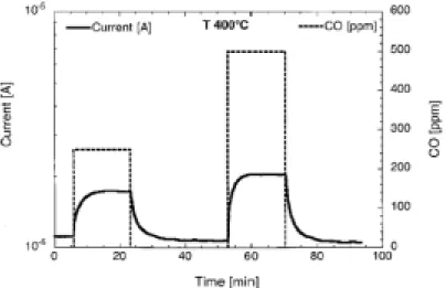
evaporating the desired commercial metal oxide powders at high temperature10-14. For example, Gas sensors have been fabricated using the SnO2 nanowires11. The
responses of the sensors have been characterized for gaseous polluting species like CO and NO2 for environmental applications, as well as for ethanol for breath
analyzers and food control applications. The response of the current flowing through the SnO2 nanowires when two square concentration pulses of CO (250 and 500 ppm)
are fed into the test chamber, at a working temperature of 400 °C and 30% RH. The electric current increased for about 60% and 100% with the introduction of 250 and 500 ppm CO, respectively which is shown in figure 1.5.
Figure 1.5 Response of the SnO2 nanobelts to CO at a working temperature of 400 °C
and 30% RH. (Ref. 11)
Conducting polymers have attractive features such as mechanical flexibility, ease of processing, and modifiable electrical conductivity. Polyaniline/poly-(ethylene oxide) (PANI/PEO) nanowire sensors that can detect NH3 gas at concentrations as
low as 0.5 ppm with rapid response and recovery time15. The measured current versus time curves, which reflect the gas-concentration dependence of the temporal conductance behavior, as shown in figure 1.6. The higher current changed as the higher NH3 gas flowed.
Figure 1.6 Measured time-dependent current through an individual CPNW sensor upon exposure to NH3 gas. The nanowire device being tested was about 335 nm in
diameter. (Ref. 15)
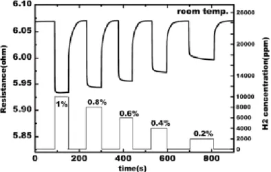
Pd nanowires have been studied to detect hydrogen gas due to safety reasons 17. The sensor based on resistance change of Pd nanowires upon hydrogen incorporation. The measured electrical resistance versus time curves exhibited sharp decreases upon hydrogen injections. The electrical resistance change is dependent on hydrogen concentration, as shown in Figure 1.7. The higher current changed as the higher H2
Figure 1.7 Sensor resistance responses for hydrogen concentration varied in a range from 0.2 to 1% by pulses. (Ref. 17)
All applications of nanowire sensor are listed in the following table 1-1. Material of nanowire sensor Application
Silicon pH sensor, bio-sensor, DNA sensor and virus sensor
Metal oxide gas sensor
Polymer gas sensor and bio-sensor
Metal gas sensor
Table 1-1 The applications of various materials of nanowire sensor.
1.3 Motivation
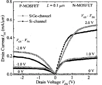
The more applications were observed for the silicon nanowire form table 1-1 since the silicon dioxide can effectively passivate surface dangling bonds, and at the same time can be chemically modified through the well known silanol chemistry to provide surface functionalization and, therefore, selectivity for particular analytes. The high surface-to-volume ratio of nanowires results in a strong dependence of carrier concentration on charge transfer from the surface and changes in nanowire conductance. For the study of SiGe field effect transistor19, we could found that the
higher current change as the same gate voltage applied (shown in figure 1.8). However, the mechanism for the silicon nanowire sensor is detecting the surface charge as the molecular stays on it. This result point out SiGe nanowires maybe have higher change in electrical property at the same chemical species bonding to surface of nanowires. Therefore, if we used the SiGe nanowire instead of Si nanowire, we would get higher current change at the same bio-molecular bound on the surface. It means we would have higher sensitivity for SiGe nanowire instead of Si nanowire.
Figure 1.8 Drain current of N- and P-MOSFETs are improved with Si/SiGe-channel. (Ref. 19)
Chapter 2
Fabrication of Nanowires
2.1 Introduction
Various approaches for growing nanowires, including (1) lithography with photons in UV, DUV, EUV and X-ray spectrum20 (2) machining using AFM, STM, NSOM21 (3) nanoimprint lithography22 (4) spacer formation23 (5) vapor state synthesis24 (6) vapor-liquid-solid growth(VLS) approach25 (7) electrochemical deposition26 (8) Laser Ablation27.
2.1.1 Lithography with Photons
In photon and particle-based lithography, by using nonlinear resists, near-field phase shifting or topographically directed technology, it has been possible to achieve sub-50nm feature. For example, EBL has demonstrated the ability to achieve 20nm width nanowires with 60nm height. Height is often limited by the lift-off process. Extreme ultraviolet light (EUV) lithography has generated 38nm patterns20.
2.1.2 Machining Using AFM, STM, NSOM
In 1990, J. A . Dagata et al. proposed the tip-induced anodic surface oxidation by using scanning probe lithography (SPL) to define nano- patterns on the semiconductor surface, as shown in Figure 2.1. AFM, STM and NSOM and the like are called SPM. The operation mechanism is in an environment humidity control when approximately 50% and the sample surface attaches a water thin film when the probe contacts this water thin film. Take the probe as negative electrode and take the sample surface as the positive electrode then the water molecule can start to ionization and produces the partial region oxide compound with the probe under- earth sample surface. The probe produces the electric field can along with the distance of sample
surface to attenuation, the oxidation stops immediately when the electric-field intensity is smaller than 109 V/m21. The oxide compound growth speed gives the probe bias to have the enormous relations. In the process by way of program configure, but fine holds controls scans the probe the displacement, carries on oxide compound of the specific line to grow, then achieves the micro region design forming the goal, this is scanning probe lithography technique to apply to the lithography at the beginning of shape.
Figure 2.1 Schema of Scanning Probe Lithography (SPL).
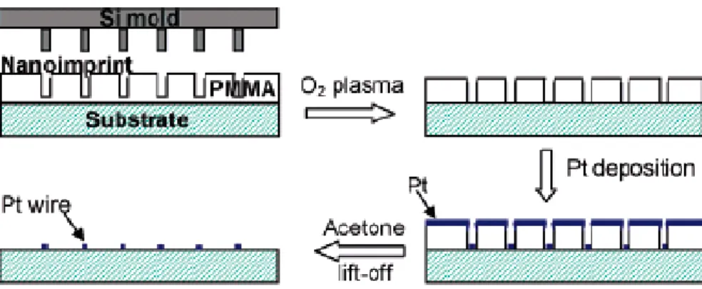
2.1.3 Nanoimprint Lithography (NIL)
Nanoimprint lithography is a novel method of fabrication nanometer scale patterns. In previous report22, the single crystalline Si nanowire structures are fabricated as a mold for producing high surface area Pt wire. PMMA are spun on substrate and are used as imprint resist. The process flow for nanoimprint patterning is
shown in Figure 2.2.
Figure 2.2 Schema of imprint process. (Ref. 22)
2.1.4 Spacer Formation
Controlled deposition and size reduction, which involves deposition on cleaved edges, or oxidation, followed by anisotropic etching forming spacers This process provides a density increase as well as size reduction. It can be used to pattern silicon fins for double-gate MOSFETs shown in Figure 2.3.
Figure 2.3 Schema of spacer process. (Ref. 23)
2.1.5 Vapor State Synthesis
Vapor state synthesis of single-crystalline freestanding Ag nanowire has been reported by Kim′s group24. Their synthetic method is unique in that it uses only a single reactant, Ag2O, without using any templates or catalysts. In a typical synthesis,
Ag2O powder was placed in an alumina boat in the middle of horizontal quartz tube
furnace. The NWs were grown at a few centimeters downstream from the precursor on a Si substrate. At high temperature (T = 900°C-1000°C), the precursor vapor was carried downstream by the flow of Ar to a lower temperature zone (T = 500°C), where Ag NWs were grown.
2.1.6 Vapor-Liquid-Solid (VLS) Growth Approach
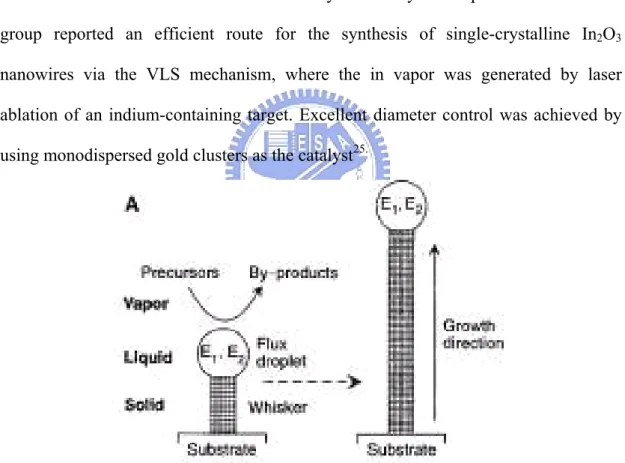
Vapor state synthesis grown nanowires lack a diameter-control mechanism. Diameter of nanowires can be controlled by the catalyst nanoparticle size. Zhou′s group reported an efficient route for the synthesis of single-crystalline In2O3
nanowires via the VLS mechanism, where the in vapor was generated by laser ablation of an indium-containing target. Excellent diameter control was achieved by using monodispersed gold clusters as the catalyst25.
Figure 2.4 Mechanism of spacer process. (Ref. 25)
2.1.7 Electrochemical Deposition
Anodized aluminum oxide (AAO) film is a kind of poriferous material. In previous report, the free-standing Pd nanowires were prepared by electrodeposition
into the nanopores of anodized aluminum oxide (AAO) films. The free-standing Pd nanowires were formed after removing the AAO template.
2.1.8 Laser Ablation
A method combining laser ablation cluster formation and VLS growth was developed for the synthesis of semiconductor nanowires27. In this process, laser ablation was used to prepare nanometer diameter catalyst clusters that define the size of wires produced by VLS growth. This approach was used to prepare bulk quantities of uniform single-crystal Si and Ge nanowires with diameters of 6 to 20 and 3 to 9 nm, respectively, and lengths ranging from 1 to 30 micrometers. The schematics are shown in Figure 2.5. In the Laser ablation technique, (1) Laser ablation with photons of energy hν of the SiFe target creates a dense, hot vapor of Si and Fe species. (2) The hot vapor condenses into small clusters as the Si and Fe species cool through collisions with the buffer gas. The furnace temperature is controlled to maintain the Si-Fe nanocluster in a liquid state. (3) Nanowire growth begins after the liquid becomes supersaturated in Si and continues as long as the Si-Fe nanoclusters remain in a liquid state and Si reactant is available. (d) Growth terminates when the nanowire passes out of the hot reaction zone onto the cold finger and the Si-Fe nanoclusters solidify.
The side-wall spacer technique is the cheapest and easier controlled technique to fabricate the nanowires. In the following, we would use the cheapest technique side-wall spacer to fabricate the Poly-Si/SiGe nanowire and discuss the drive current and sensitivity enhancement of Poly/SiGe nanowire with different Ge concentrations.
2.2 Experiment
The side-wall spacer formation is an easy process for nanowire fabrication with the advantages of high-yield and low-cost. The method only using the combination of the conventional lithography and processes technology was demonstrated without complex processes such as EBL, SPL and VLS etc. In the beginning, a p-type (100)-oriented bare silicon wafer with 1-10Ω-cm resistivity was prepared.
1. After standard RCA cleaning, 980℃ Wet Oxidation was performed for 1 hours to grow the bottom oxide as an insulator oxide by ASM/LB45 Furnace system. The thickness of the oxide is 3000Å which was shown in Figure 2.6.
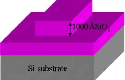
2. Mask #1: Define the active area. We etched the oxide 1000 - 1500 Å by dry oxide etcher (TEL 5000) after Mask I defined. Then, a 1500 - 2000 Å oxide step was formed shown in Figure 2.7.
3. Following standard RCA clean, we deposited 150Å amorphous Si film on bottom oxide in the condition of 650℃ and 160 mTorr. The process increased adhesion between SiGe film and SiO2 layer shown in Figure 2.8.
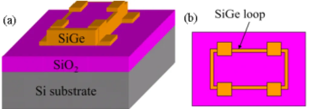
4. Then, 500-1000 Å SiGe films with different Ge concentrations were deposited with the ultra-high-vacuum chemical vapor deposition (ANELAVA SiGe UHV-CVD) at 650℃. Also, the 800 Å poly-Si film was deposited, too. The structure is shown in Figure 2.9.
5. We defined the S/D contact regions with Mask II, and etched the whole height of the SiGe film (20% over etched) and the poly-Si film (20% over etched) by TCP
poly etcher in the follows. Only the S/D and SiGe/poly-Si deposited in the sidewall spacer were stayed. The residual SiGe film is what we want – SiGe nanowire. The structure is shown in Figure 2.10.
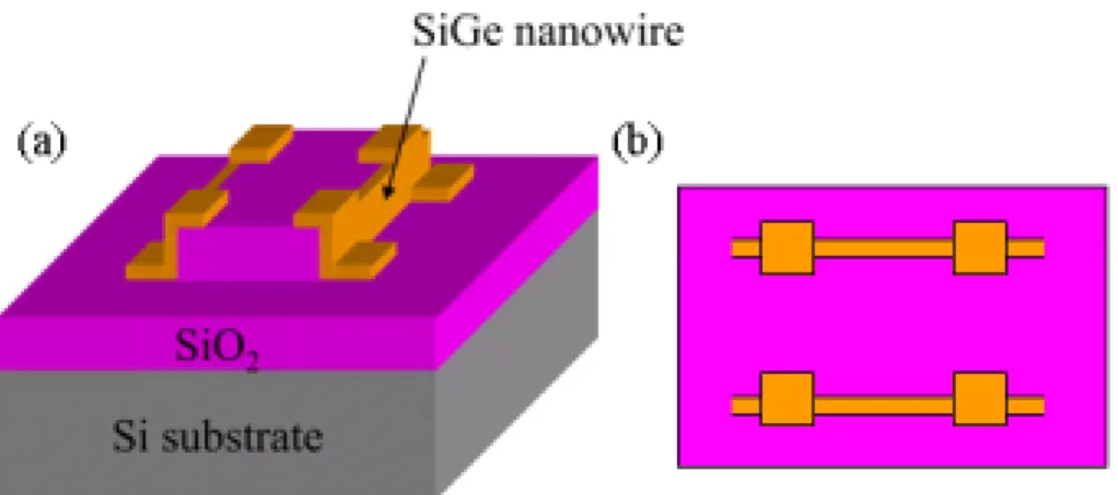
6. Next, we etched each pair of the parallel SiGe NW by TCP poly etcher after Mask III was defined. Thus, the poly-Si/SiGe nanowires were isolated. The structure is shown in Figure 2.11.
7. Finally, the aluminum was then deposited with a thickness of 5000 Å by thermal coater. Mask IV was used to reserve the S/D region, and then 400℃ sintering 30 min was done shown in Figure 2.12.
8. Al sintering at 430℃ in N2 ambient for 25 minutes.
Figure 2.6 3000Å SiO2 layer was grown on Si substrate.
.
Figure 2.8 150Å Amorphous Si layer is deposited on SiO2 layer.
Figure 2.9 SiGe films with different Ge concentration were deposited on α-Si layer.
Figure 2.10 The definition of the S/D region and nanowire. (a) The 3-D view (b) The top view
Figure 2.11 Remove one side of the parallel SiGe spacer to cut off the leakage current (a) The 3-D view (b) The top view.
Figure 2.12 Defined Al contact pad. (a) The 3-D view (b) The top view.
2.3 The Dimension of Nanowires
The dimension of nanowire was controlled by the deposition for the width and the step of oxide for the height. In order to etch the poly-Si or SiGe film clearly, we added the 20% over-etching at the step of dry etching. The dimensions of poly-Si nanowires and SiGe nanowires with different Ge concentrations were observed by Scanning Electron Microscope (SEM) after dry etching, which is shown in Figure 2.13 (a) and (b) show the poly-Si nanowire with 174 nm in height and 76.9 nm in width, (c) shows the poly-Si0.93Ge0.07 nanowire with 280 nm in height and 108 nm in
width, and (d) shows the poly-Si0.89Ge0.11 nanowire with 86 nm in height and 44 nm in
width respectively.
Figure 2.13 (a) The top view of poly-Si nanowire. (b) The cross-section view of poly-Si nanowire with 174 nm in height (H) and 76.9 nm in width (W). (c) The Si0.93Ge0.07 nanowire with H = 280 nm and W = 108 nm. (d) The Si0.89Ge011 nanowire
with H = 86 nm and W = 44 nm.
2.4 Results and Discussions
The electrical properties of poly-Si/SiGe nanowires were measured by an Agilent 4156C semiconductor parametric analyzer. We swept the ID-VD from –5 V to 5 V,
and changed the bottom gate VG = –10 V, –5 V, 0V, 5V and 10V, respectively. In
order to make sure that the measured current came from the nanowire, we made a test structure which the diagram is shown in Figure 2.14 (b). The current measured between the two 3 um distance isolated pads without nanowire is few pA which shows in Figure 2.14 (a). The ID-VD curve of Poly-Sinanowire with 15 um in length is
shown in Figure 2.14 (c) by different bottom gate voltages applied. It is observed that the undoped poly-Si nanowires show the property of p-type like. The drive current increased as the bottom gate applied negative voltage, however, the drive current decreased as the bottom gate applied positive voltage. The result could be the surface charge. The same phenomenon was also found in SiGe nanowires, too. The ID-VD
curve of Si0.93Ge0.07 nanowire with 15 um in length is shown in Figure 2.14 (d). The
ID-VD curve of Si0.89Ge0.11 nanowire with 15 um in length is shown in Figure 2.14 (e).
Because of the drive current higher than the leakage current (2 pA), we could make sure that what we measured were all the drive currents. For comparing the current in different sizes of nanowire, we considered the nanowire as a resistance. Let us consider the following equation (1).σ is the conductor, I is the current, L is the length, V is the applied voltage and A is the area of nanowire. Thus, we should normalize the length and area of the different nanowires by multiplying the L and dividing the A. The normalized current with bottom gate applied –15V is shown in Figure 2.15 (f). The higher drive current is achieved for SiGe nanowire instead of Poly-Si nanowire. Also, the drive current increased as the Ge concentration increased. It is useful for detecting the molecular on the nanowire.
Figure 2.14 (a) The leakage current of the isolated pad without nanowire. The current is about 2 pA. (b) The diagram for leakage current test structure. (c) The drive current of Poly-Si nanowire with 15 um in length. (d) The current of Si0.93Ge0.07 nanowire
with 15 um in length. (e) The current of Si0.89Ge0.11 nanowire with 15 um in length. (f)
The normalized current of Poly-Si and SiGe nanowires. The higher drive current is obtained by SiGe nanowire with higher Ge concentration.
In the follows, we discuss the influence of implantation. Two conditions are considered. The first one is only the Source/Drain implanted. The PR was used for hard mask to stop the channel be implanted. Boron was doped with doses 5x1015 cm-2 at energy 10 keV. Activation annealing at 950℃ in N2 flow was then employed for 30
minutes after PR stripped. The diagram is shown in insert of Figure 2.15 (c).
The ID-VD curve of Si0.89Ge0.11 nanowire with 5 um in length is shown in Figure
2.15 (a) by different bottom gate voltages applied. It is observed that the undoped poly-Si nanowires show the property of p-type like, too. The same phenomenon was also found in Poly nanowires. The ID-VD curve of Poly-Sinanowire with 5 um in
length is shown in Figure 2.15(b). For comparing the current of Poly-Si and SiGe nanowires, we normalized the current by the same way. The higher current was found in SiGe nanowire instead of Poly-Si nanowire shown in Figure 2.15 (c).
The second condition: both source/Drain and nanowire channel were implanted by Boron with doses 5x1015 cm-2 at energy 10 keV. Activation annealing at 950℃ in N2
flow was then employed for 30 minutes after ion implantation. The diagram is shown in the insert of Figure 2.15 (f). Figure 2.15 (d) and Figure 2.15 (e) show the current of Si0.07Ge0.11 nanowire and Poly silicon nanowire with 15 um in length. Both the current
of SiGe and Poly-Si nanowire increased to the level of uA. The normalized current is shown in Figure 2.15 (f). The higher drive current is also achieved for SiGe nanowire.
Figure 2.15 (a) and (b) shows the drive current of Si0.89Ge0.11 and Poly-Si nanowire
with 5 um in length after S/D implant. (c) The normalized current of Poly-Si and Si0.89Ge0.11 nanowires after Source/Drain implanted. The insert picture is the diagram
of nanowire with PR covered. (d) and (e) shows the drive current of Si0.89Ge0.11 and
Poly-Si nanowire with 15 um in length after S/D and channel implant. (e) The normalized current of Poly-Si and Si0.89Ge0.11 nanowires after Source/Drain and
The serial test structure was used to know the contact resistance between aluminum and the SiGe/Poly-Si pads, which diagram is shown in the insert of Figure 2.16 (a). The micro wire with 5 um in length and 5 um in width is connected to each pad, and the pad dimension is 100 um x 100 um. The Boron implantation and activation annealing were the same as the conditions above. We measured the current for one block distance to eleven block distance, and calculated the resistance of them (voltage divide current). After plotting the resistance v.s. the block distance shown in Figure 2.16 (a), then the linear fit line is calculated on it. The intersection of the y-axial and fit line was the resistance without any micro wire, which meant the contact resistance between the aluminum and Poly-Si pads. The clearly view is shown in Figure 2.16 (b). The same process was used to measure the contact resistance of Al/Si0.89Ge0.01 shown in Figure (c) and (d). The contact resistance is 31.702 Ω for
Poly-Si, and the contact resistance is 71.57 Ω for Si0.89Ge0.11. However, the resistance
of Poly-Si with 11 pad distance is 31 kΩ which is higher than the resistance of SiGe (22.7 kΩ). The lower wire resistance and higher contact resistance of SiGe were observed in the experiment.
Figure 2.16 (a) and (b) show the resistance V.S. the contact pads of Poly-Si/Al. (c) and (d) show the resistance v.s. the contact pads of Si0.89Ge0.11/Al. The intersection of
the y-axial and fitted line is the contact resistance between the aluminum and Poly-Si/SiGe pad.
2.5 Summary
The side-wall spacer Poly-Si/SiGe nanowires were successfully fabricated by the side-wall spacer technique on Si wafer. The SEM image is used to know the dimension of nanowire. In order to normalize the drive current of nanowires, we consider the nanowire as a resistor. The conductance is chosen for comparison between the nanowires. The higher drive achieved of SiGe nanowire instead of Poly-Si nanowire, and the higher current obtained for the SiGe nanowire with higher Ge concentration. The reason for less improvement of conductance after ion implantation may be that the implant dominates the current and decreases the influence of Ge element. However, the drive current of Si0.89Ge0.11 nanowire still has
50% improvement than Poly-Si nanowire after ion implantation. The test structure of serial contact pad with 5 um length micro wire was used to compare the contact resistance of SiGe and Poly-Si. The higher contact resistance and lower conductance are the properties of SiGe nanowire.
Chapter 3
Electrical Properties of SiGe Film with Various Oxidation Conditions
3.1 .1 An Overview of the Applications of High Mobility SiGe Alloy
As the channel length of metal-oxide-semiconductor field effect transistors (MOSFETs) is deeply scaled down to sub-100 nm, enhancement of the carrier mobility in the channel is desired for improving the performance of complementary MOS (CMOS) circuits28. For this purpose, Ge is a promising channel material for MOSFETs because of high mobility of both the electrons and holes. Enhanced device performances have been demonstrated by using a strained Si channel grown upon a relaxed (SiGe) substrate29, where the electron mobility is increased due to the reduced intervalley phonon scattering30. However, at lower Ge content, only moderate increase in hole mobility could be achieved in strained Si compared to bulk Si31. On the other hand, with high Ge content (83%), SiGe channel high hole mobility enhancement in PMOSFETs can be realized32. To achieve the highest enhancement, pure Ge channel is attractive.
3.1.2 Ge Condensation Process in SiGe Film
Conventionally, relaxed Si1-xGex film with high Ge content has been obtained by
growing compositionally graded Si1-xGex much thicker than the critical thickness in
order to introduce dislocations to relax strain in Si1-xGex layer33. Although the density
of dislocations in the relaxed SiGe layer by this approach has been greatly reduced over time, the control of dislocations is still challenging and requires optimization for dislocation suppression. In addition, the thick Si1-xGex films need for strain relaxation
10% germanium increment per micron) poses a serious bottleneck for throughput34. An approach to achieve high Ge content in relaxed Si1-xGex layer has been
reported that takes the advantage of the selective removal of Si atoms from SiGe film by Si1-xGex thermal oxidation35. When supply of Si atoms diffused from the SiGe to
the oxidation interface meets the consumption of Si atoms during oxidation, only Si atoms would be oxidized because Si oxidation is preferred to Ge oxidation36, which leads to an increased Ge content in the Si1-xGex layer as the film is thinned down.
3.1.3 Mechanism of SiGe Oxidation
The oxidation of SiGe thin films has been demonstrated at several laboratories37-40. In these cases, enough Ge on the oxidation of Si had to be snow-plowed in order for oxidation enhancement to be observed. They proposed that breaking of the weaker Si-Ge bound as compared with Si-Si explain the rate enhancement. This may only be the last event, not necessarily controlling. For example, represents a steady-state situation in which Si-Si bonds must still be broken below the Ge-enriched layer to supply the needed Si flux to the interface to maintain the high oxidation rates. Attention should be focused on the growth interface and interactions there since the Ge effect is found only in the initial and linear regime of oxidation. In all cases reported so far, it is shown that Si is preferentially oxidized and only one Ge-rich layer is formed at the oxide/substrate interface for SiGe with a Ge concentration below 50%. On the other hand, there are two oxide layers formed after oxidation for SiGe with Ge concentration above 50%.
According to the theory binary alloy oxidation41-42, the oxide growth will depend on the alloy composition. For the case of the SiGe alloy, Si is more reactive than Ge. The reason is the large difference between the heat of formation of SiO2 (-204
only silicon is oxidized initially. Ge is completed rejected from the oxide and piles up at the oxide/substrate interface. On the other hand, oxygen concentration at the oxidation front decreases with the oxide thickness increases. Then, the decreasing oxygen concentration at the oxidation front counteracts the effect of increasing Ge concentration in the Ge-rich SiGe layer so that Ge is not oxidized during the entire oxidation process.
For SiGe with high Ge concentration (> 50%), Si and Ge will be oxidized during the oxidation process. In alloys containing 50 and 75 at.% Ge, the rate of diffusion of Si to the oxide/alloy interface is sufficiently slow with respect to the rate of oxidation that it rapidly becomes impossible to grow pure SiO2 . Thus, the initial oxide formed
is a mixed (Si, Ge)O2 oxide. Eventually, the activity of oxygen at the interface
decreases because of the thickness of the oxide, resulting in a slow down of the oxidation rate. This makes it possible for Si to diffuse to the interface as fast as is required to form pure SiO2.
Eventually, oxide thickness will reach a critical value, which is proportional to the Ge concentration in SiGe film, such that the oxygen and Ge concentration at the oxide/SiGe interface are too low for Ge to be oxidized. At this stage a steady-state condition has been reached at which selective oxidation of Si succeeds and Ge piles up at the oxide/SiGe interface again. So that it is shown that Ge at the oxide/SiGe is in elemental form, while Ge at the oxide surface is in an intermediate oxidized form.
3.1.3 Oxidation Behavior of SiGe
The oxidation behavior of SiGe films has been studied to a great extent43-45. Ge is completed rejected from the oxide and piles up at the oxide/substrate interface after oxidation process. A Ge-on-insulator (GOI) was fabricated by Ge condensation
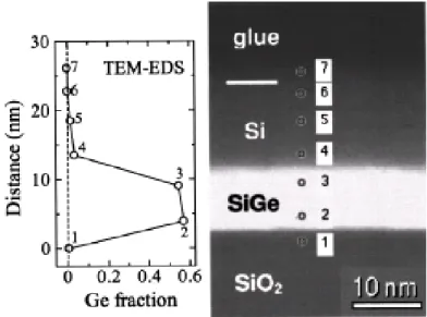
technique in previous literature46. In addition, as the thickness of SiGe layer is smaller than diffusion length of the Ge atoms, the SiGe layer will become uniform, as show in Figure 3.1. The total amount of Ge atoms in the SGOI normalized by the value before oxidation is plotted as a function of oxidation time. It is found that the amount is kept constant during oxidation. This result enables an estimation of the final Ge fraction xf
based on the simple relationship xf = xi (Ti/Tf ). Here, xi, Ti and Tf are the initial Ge
fraction, and the initial and final SGOI thicknesses, respectively shown in Figure 3.2. The conservation of Ge atoms in the SGOI layers and the low Ge concentration in the oxide layer indicate that the SiGe oxide layer rejected the Ge atoms which remained in the SGOI layer.
Figure 3.1 Scanning TEM image and Ge profile across the layers Obtained by EDS measurement. (Ref. 43)
Figure 3.2 The Ge fractions after dry oxidation. (Ref. 43)
After the oxidation process, the dislocation density significantly decreases, as show in Figure 3.3. This decrease is attributed to the high temperature annealing, lead to the rearrangement of the lattice.
Figure 3.3 Plane-view TEM observations (a) before and (b) after oxidation at the temperature of 1200 °C. (Ref. 44)
3.1.5 Motivation
SiGe oxidation is widely used in either SiGe/Si hetro-junction devices, poly-SiGe gated MOSs, or SiGe channel devices. However, the optimal oxidation condition is not known yet. In this study, we adopt different oxidation temperature, oxidation time, oxygen flow, and oxidation rate and investigate the influence on the electrical characteristics of SiGe-based p-MOSFETs.
3.2
The Process Flow of SiGe-Based P-MOSFET
P-type (Boron doped) Si substrate (100)-oriented with 1-10Ω-cm resistivity was used in this study. After initial RCA cleaning, 3000Å oxide was thermally grown at 980℃ by a horizontal furnace through wet oxidation, served as an isolation layer. After one more time RCA cleaning, a 150Å thick amorphous-Si was deposited by LPCVD at 550℃, as a buffer layer between SiO2 and SiGe film. SiGe (Ge content at
7% and 11%) film was then deposited onto amorphous-Si layer about 800 Å by UHV-CVD, shown in Figure 3.4 (a).
By means of photolithography, the active region could be defined after photo-resist was removed. After S-D and channel patterning, TCP poly etcher was employed for SiGe etching by Cl2 and HBr. Later, the main part of this study proceeds
by oxidizing the remaining SiGe part through different temperatures and times (top view shown in Figure 3.4 (b)). Oxidation parameters like temperature, time, and oxygen flow were tried in order to find out the optimum oxidation condition of SiGe channel. Moreover, pre-deposited-oxide before oxidation, oxidation rate controlling, and annealing after oxidation were also performed trying to make better electrical characteristics performance of SiGe-based p-TFT possible. All experimental factors are listed in Table 3.1 to Table 3.6.
Next, devices were dipped in BOE solution to remove surface SiO2 formed during oxidation of SiGe film. After 1000Å SiO2 deposited by PECVD served as gate
dielectic, 600℃ annealing with O2 was performed to cure the defects in gate oxide.
Then, 2000Å poly-Si was deposited by LPCVD to work as control gate, shown in Figure 3.4 (c). After gate region and channel length defined by lithography, poly-etcher and BOE solution were used for etching. Top view is shown in Figure 3.5 (d). Then, Boron was doped heavily with 5x1015 cm-2 at 10 keV. Activation
annealing at 950℃ in N2 flow was then employed for 30 minutes after ion
implantation.
Figure 3.4 (a) The stack of SiGe/SiO2/Si. (b) Top view of SiGe-S/D and channel
pattern. (c) The PE gate oxide and Poly gate were deposited. (d) Poly gate pattern.
3000Å SiO2 by PECVD was deposited as passivation layer. Lithography comes next to form contact holes. SiO2 was then etched by BOE solution for about 55
seconds. Finally, a 500 nm Al film was deposited by evaporation and then contact pads were patterned. Al sintering was performed at 430℃ for 30minutes.The detailed fabrication process flow is as follows:
2. RCA cleaning
3. Wet oxidation at 980oC for 3000Å 4. RCA cleaning
5. 150Å amorphous-Si by LPCVD 6. RCA cleaning
7. 800Å SiGe(Ge content at 7% and 11%) by UHVCVD 8. Mask #1:Define active region
9. Dry etching by TCP poly etcher 10. PR removing and RCA cleaning 11. SiGe dry oxidation
12. BOE dipped to remove SiO2
13. RCA cleaning
14. PECVD SiO2 1000Å deposition
15. Gate oxide annealing at 600o with O2 for 1hr
16. LPCVD poly-Si 2000Å deposition 17. Mask #2:Define gate and channel length
18. Wet etching by poly-etcher solution for 90 seconds 19. Wet etching by BOE solution for 25 seconds 20. PR removing
21. Boron doping of 5x1015 cm-2 at 10 keV 22. Activation at 950oC for 30 minutes 23. STD cleaning
24. PECVD SiO2 3000 angstrom deposition
25. Mask #3:Define contact hole
26. Wet etching by BOE solution for 50 seconds 27. PR removing
28. Al coating for 5000Å 29. Mask #4:Define contact pad 30. Al etching
31. PR removing
32. Sintering of Al at 430oC for 30 minutes
The cross-section view of p-type SiGe-thin-film-transistor is shown in Figure 3.5.
Figure 3.5 The cross-section view of p-type SiGe-thin-film-transistor.
Alloy concentration Oxidation condition Variable: Temperature
1000 oC 950 oC Si0.89Ge0.11 16 minutes 3750 sccm O2 flow un-oxidized Table 3.1 Influence of Oxidation Temperature Experiment
Alloy concentration Oxidation condition Variable: Time 36 minutes 16 minutes 4 minutes Si0.93Ge0.07 1000 oC 3750 sccm O2 flow un-oxidized Table 3.2 Influence of Oxidation Time Experiment
Alloy concentration Oxidation condition Variable: O2 Flow
3750 sccm 2500 sccm Si0.89Ge0.11 1000 oC 16 minutes un-oxidized Table 3.3 Influence of Oxygen Flow Experiment
Alloy concentration Oxidation condition Variable: Thickness
1000Å 500Å 300Å Si0.93Ge0.07 1000 oC 36 minutes 3750 sccm O2 flow no pre-oxide Table 3.4 Influence of Thickness of Pre-Oxide Experiment
Alloy concentration Oxidation condition Variable: Rate
950 oC 15 minutes 900 oC 30 minutes Si0.93Ge0.07 3750 sccm O2 flow
850 oC 75 minutes Table 3.5 Influence of Oxidation Rate Experiment
Alloy concentration Oxidation condition Variable: Annealling
6hrs anneal Si0.93Ge0.07
950 oC 5 minutes
3750 sccm O2 flow no annealing
3.3 Results and Discussions
Id-Vg and Id-Vd characteristics in these experiments were measured by HP4156A. In the following measurements of current, all devices were normalized to W/L = 1μ/1μ. In Id-Vg measurements, Vd was applied at (-5 V). While Id-Vd was measuring, |Vg-Vt| was set at 3V.
3.3.1 Influence of Oxidation Temperature on Electrical Properties
Figure 3.6 (a) shows Id-Vg characteristics of three different devices: un-oxidized, oxidation at 950 , and oxidation at 1000 . Si℃ ℃ 0.89Ge0.11 film was used in these
experiments, and both of the oxidized devices were oxidized for 16 minutes with 3750 sccm O2 flow. It can be seen that both oxidized devices show superior electrical
performance than the un-oxidized one by higher On/Off ratio. The device of 1000 ℃-oxidized shows even higher on current than the one of 950 ℃-oxidized one while both devices have roughly the same off state current.
Figure 3.6 (b) shows Id-Vd characteristics which are consistent with the prediction: the device oxidized at 1000 ℃ has highest Id of the three devices – 2.58µA at Vd = (-6)V. 950℃- oxidized device has 1.83 µA, and the un-oxidized one has 0.40µA. It was known that since SiGe got oxidized, concentration of Ge would be increased, and then mobility would also get enhanced which resulted in a higher on state current, On/Off ratio gets improved then. With higher oxidation temperature, the rate of oxidation would be higher, which made more Si in SiGe film oxidized. Then the mobility would be even higher, and better performance was achieved.
Figure 3.6 (a) Id-Vg characteristics of different oxidation temperatures. (b) Id-Vd characteristics.
3.3.2 Influence of Oxidation Time on Electrical Properties
Figure 3.7 (a) shows Id-Vg characteristics of four different devices: un-oxidized, oxidized for 4 minutes, oxidized for 16 minutes, and oxidized for 36 minutes, respectively. Si0.93Ge0.07 film was used in these experiments. All of the oxidized
devices were oxidized at 1000oC with 3750 sccm O2 flow. From the diagram, the
trend of the curves indicates that longer oxidation time results in higher on state current. Besides, after calculation, the On/Off ratio of 36m-oxidized, 16m-oxidized, and 4m-oxidized is 3.3, 1.6, 1.5 times higher than that of the un-oxidized device, respectively. Due to the same reason as described previously, in the longer oxidation
time devices, more amount of Si was oxidized and then higher Ge concentration was achieved. Figure 3.7 (b) depicts Id-Vd characteristics for devices with different oxidation times. As predicted, 36m-oxidized device has highest on current, which is 5.08µA at Vd = (-8)V. For the other devices, they are 1.52µA, 0.75µA, and 0.61µA for 16m-oxidized, 4m-oxidized, and un-oxidized devices, respectively.
It is presumed that unless Si in the SiGe layer is fully oxidized, the performance of the SiGe-based p-MOSFET would always be improved with the increasing of oxidation time since the positive correlation between the amount of oxidized Si and the mobility of SiGe channel.
Figure 3.7 (a) Id-Vg characteristics after different oxidation times; the temperature is 1000℃ (b) Id-Vd characteristics.
3.3.3 Influence of Oxygen flow on Electrical Properties
Si0.89Ge0.11 film was used in this experiment. Devices were oxidized at 1000oC for
16 minutes. Figure 3.8 (a) depicts Id-Vg characteristics of devices with different oxygen flows during oxidation: 3750 sccm, 2500 sccm, and un-oxidized. The device under larger oxygen flow shows larger on-state current and lower-off state current, which are undoubtedly better than the devices oxidized under 2500 sccm oxygen flow and the un-oxidized one. It is supposed to be contributed by more Si being oxidized, as discussed before. The On/Off ratios of 3750sccm-device and 2500sccm-device are 5.89 and 1.86 times higher than the un-oxidized one. As to Id-Vd characteristics, which is shown in Figure 3.8 (b), the device with 3750 sccm O2 flow has 2.56µA at
Vd = (-6)V. The devices with 2500 sccm O2 flow and un-oxidized have 1.83µA and
0.43µA, respectively. From the experiments above, the amount of oxidized Si explains the improvement of electrical charateristic performance well. In the following study, several different oxidation conditions were applied, and some other results would be achieved.
Figure 3.8 (a) Id-Vg characteristics after different oxygen flow rates at 1000℃ (b) Id-Vd characteristics.
3.3.4 Influence of the Thickness of Pre-oxide on Electrical Properties
As it is known that the oxidation rate would decreases with increasing the oxidation time, a new experiment is designed to investigate the influence of the initial oxidation rate on electrical performance of SiGe-based TFT. SiO2 was deposited onto
SiGe film first by PE-CVD just after UHV-CVD SiGe film deposited. The thicknesses of SiO2 were 300Å, 500Å, and 1000Å, respectively, and a non-pre-oxide device was
also fabricated. Si0.93Ge0.07 was used in this experiment and oxidation was performed
at 1000oC for 36 minutes with 3750 sccm O2 flow. Figure 3.9 (a) depicts Id-Vg
getting higher while the thicknesses of pre-oxide is getting larger, which is 2.6, 1.9, 1.7 times higher than that of non-pre-oxide device, respectively. But on the other hand, the on-state current decreases. It is presumed that less amount of Si in SiGe film would be oxidized owing to thicker pre-oxide existing that results in lower on current. As shown in Figure 3.9 (b), Id at Vd = (-8 V) of non-pre-oxide, 300 Å, 500 Å, and 1000 Å are 5.46µA, 2.79µA, 1.07µA, and 0.95µA, respectively. But there is still benefit from depositing pre-oxide. Since the oxidation rate was lowered by pre-oxide, the segregation Ge atoms would distribute evenly in SiGe channel, which lowers the off-state current, and results in a higher On/Off ratio.
Figure 3.9 (a) Id-Vg characteristics with different thicknesses of pr-oxide deposited before oxidation ; the temperature is 1000℃ and the time is 36 min. (b) Id-Vd characteristics.
3.3.5 Influence of Oxidation Rate on Electrical Properties
In the previous study, it is concluded that under lower oxidation rate, SiGe-based p-TFT would achieve better On/Off ratio performance. However, the amount of oxidized Si in last experiment was still a variable. The factor of the amount of oxidized Si was removed by a new designed method. Several oxidation conditions were performed first and the thickness of SiO2 was measured. Three oxidation
conditions of roughly the same thickness of SiO2 were selected. They are 950oC 15
minutes, 900oC 30 minutes, and 850oC 75 minutes, respectively, which indicate the same amount of Si oxidized. Si0.93Ge0.07 was used in this experiment and oxidation
was performed with 3750 sccm O2 flow. Figure 3.10 (a) depicts Id-Vg characteristics
at Vd = -5 V. On-state current of the three devices almost equals, but the device with lower oxidation rate has lower off-state current, which supports our conclusion from the previous study. In Figure 3.10 (b), it is shown that the on-state current of the three devices are also almost the same at about 2.1 ~ 2.3 µA. As predicted, same amount of oxidized Si results in same Id. Slow oxidation rate makes Ge atoms distribute evenly and then makes lower off-state current which achieves a higher On/Off ratio.
Figure 3.10 (a) Id-Vg characteristics of different oxidation rates. (b) Id-Vd characteristics.
3.3.6 Influence of Annealing after Oxidation on Electrical Properties
In the final section, annealing was performed after SiGe film oxidation. Si0.93Ge0.07 was used in this experiment and oxidation was performed at 950oC for 5
minutes with 3750 sccm O2 flow. Device was annealed for 6 hours after oxidation,
and a non-annealing device was also fabricated. Figure 3.11 (a) depicts Id-Vg characteristics at Vd = -5 V. The On/Off ratio of 6 hrs-annealing-device was slightly improved by 1.4 times than non-annealing device. In Figure 3.11 (b), Id-Vd characteristic diagram is shown. Nearly 80% Id improvement is achieved by annealing for 6 hours, which is 3.90µA, in comparion with 2.17µA of the
non-annealing device. It is supposed that annealing at high temperature cures the defects in the SiGe channel, and facilitates evenly distribution of Ge in SiGe channel and thus improves the on-state current and the leakage current.
Figure 3.11 (a) Id-Vg characteristics of annealing applied. (b) Id-Vd characteristics.
3.4 Summary
It is found that all the electrical characteristics such as On/Off ratio, and on state current would get improvement after the SiGe channel was oxidized. This is because after oxidation, Si atoms in SiGe channel would be combined with O atoms to form SiO2 while Ge atoms would be separated from that. The more amount of Si in the