Studies Of High Performance Metal Gate
Low Temperature Poly-Silicon Thin Film
Transistor
:
:
Studies Of High Performance Metal Gate Low
Temperature Poly-Silicon Thin Film Transistor
Studies OF High Performance Metal Gate
Low Temperature Poly-Silicon Thin Film
Transistor
Student: Hsiang-Ku Shen
Advisor: Dr. Albert Chin
Department of Electronics Engineering & Institute of Electronics
Nation Chiao Tung University
Abstract
We have integrated a Metal gate into Poly-Silicon (LTPS)
thin-film transistors (TFTs) with high –
gate dielectric. We
use Ytterbium ( Yb , has the lowest work-function in Lanthanide
series metal
2.6 eV ) for NMOS. We get good TFT
performance in NMOS, such as a low threshold voltage, a high
drive current, a low subthreshold slope, high gate–dielectric
breakdown voltage, and a very good on/off current ratio. The
good performance is related to the low work-function metal,
Ytterbium, makes the threshold voltage lower successfully and
small equivalent oxide thickness by high
dielectric material.
This was achieved without special crystallization steps, we only
use furnace to crystallize.
Contents
Abstract (in Chinese)
………IAbstract (in English)
………...IIContents
……….IIIFigure Captions
………..VChapter 1 Introduction
1.1 Thin Film Transistor….
………..………….….11.2 Overview Of Polycrystalline Silicon Thin Film Transistor
Technology………...1
1.3 Poly-Silicon Recrystallization Methods………..……….4
1.3.1 Solid-Phase Crystallization Method………..5
1.3.2 Excimer Laser Annealing Crystallization Method………6
1.3.3 Metal-Induce Lateral Crystallization Method………...7
1.3.4
Rapid Thermal Annealing Crystallization Method………8
1.4 Gate Dielectric Film Option…...………..9
1.4.1 Original Gate Oxide Growth Technology……….….9
1.4.2 Reason For Using LaAlO
3For Gate Dielectric Film….………….10
1.6 Motivation……….13
1.7 Thesis Outline……….15
Chapter 2 The Experimental Steps
2.1
The Fabrication Steps……….16
2.2 The Structure Of Fabrication………..17
Chapter 3 Result & Discussion
3.1 Method Of Device Parameter Extraction………...24
3.1.1 Determination Of Threshold Voltage………...24
3.1.2 Determination Of Sub-threshold Slope………...25
3.1.3 Determination Of Field Effect Mobility………..26
3.1.4 Determination Of ON/OFF Current Ratio………..26
3.2 Experimental Data Result & Discussion………27
Chapter 4 Conclusion
………43References
……….44Figure Captions
Chapter 1 Introduction
Fig 1.1 the structure of Poly-Silicon on Metal Oxide
Fig 1.2 The Fermi level pining effect of Si-Hf bond Fig 1.3 The Fermi level pining effect of Si-O-Al bond
Chapter 2 Experimental Steps
Fig 2.1 Step 1 Fig 2.2 Step 2 Fig 2.3 Step 3 Fig 2.4 Step 4 Fig 2.5 Step 5 Fig 2.6 Step 6 Fig 2.7 Step 7 Fig 2.8 Step 8 9 Fig 2.9 Step 10 Fig 2.10 Step 11 Fig 2.11 Step 12 Fig 2.12 Step 13 Fig 2.13 Step 14 Fig 2.14 Step 15
Chapter 3 Result & Discussion
Table 1 The primary parameter comparison of different structure thin film transistor
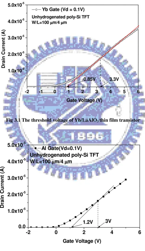
Fig 3.1 The threshold voltage of Yb/LaAlO3 thin film transistor
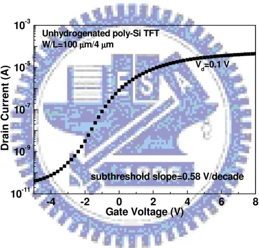
Fig 3.2 The threshold voltage of Al/LaAlO3 thin film transistor
Fig 3.4 The mobility of Yb/LaAlO3 thin film transistor
Fig 3.5 The drain current of Yb/LaAlO3 thin film transistor at different voltage
Fig 3.6 The C-V measurements of Yb/LaAlO3 thin film transistor
Fig 3.7 The drain current of Al/LaAlO3 thin film transistor at Vg=1V.
Fig 3.8 The drain current of Yb/LaAlO3 thin film transistor at Vg=1V
Fig 3.9 The drain current of Al/LaAlO3 thin film transistor at Vg=3V.
Fig 3.10 The drain current of Yb/LaAlO3 thin film transistor at Vg=3V
Fig 3.11 The drain current of Al/LaAlO3 thin film transistor at Vg=5V
Fig 3.12 The drain current of Yb/LaAlO3 thin film transistor at Vg=5V
Fig 3.13 The comparison of drain current at different gate voltage between Yb-gate and Al-gate
Fig 3.14 The breakdown voltage of Yb/LaAlO3 thin film transistor Fig 3.15 The gate voltage shift of Yb/LaAlO3 thin film transistor
Chapter 1
Introduction
1.1 Thin-Film Transistors
A transistor whose active, current-carrying layer is a thin film (usually a film of silicon), in contrast to MOSFETs, which are made on Silicon wafers and use the bulk-silicon as the active layer. In a flat-panel display, light must be able to pass through the substrate material to reach the viewer. Opaque silicon wafers obviously will not be suitable for these transmissive displays. Glass is the most commonly used starting substrate because it is highly transparent and is compatible with conventional semiconductor processing steps. Since glass is not a semiconductor like silicon, a thin film of silicon is deposited on top and the transistors are fabricated using this thin layer. Hence, the name "thin-film transistor."
1.2 Overview of Polycrystalline Silicon Thin-Film Transistors
Technology
Polycrystalline silicon thin-film transistors (TFTs) have been investigated extensively for their use on the peripheral driving circuits in active matrix liquid crystal displays (AMLCDs) [1], high-density static random access memories (SRAMs) [2][3], linear image sensors [4], thermal printer heads [5], liquid crystal shutter arrays for printers [6], photodetector amplifier [7], and nonvolatile memories [8] ,etc.
Traditionally, AMLCDs were fabricated using hydrogentated amorphous silicon ( -Si:H) TFTs for the pixel switching devices [9]. The -Si:H TFTs have many advantages, particularly its compatibility with low temperature process on large glass substrate and high off-state resistivity which result a low leakage current. However, the low electron field effect mobility in -Si:H TFTs has limited the technology development for AMLCDs application. To integrate the switching elements with the driving circuits on the same substrate is very desirable not only to reduce the cost but also to improve the system performance. Therefore, poly-Si TFTs, which provide higher electron field effect mobility, have been developed as a substitute for -Si:H TFTs. Besides, poly-Si TFTs have other advantages such as lower photocurrent, CMOS capability and better reliability [10], thus enables the integration of peripheral circuits as well as the active-matrix switching elements on the same substrate.
It should be noted that ‘Poly-Silicon’ covers a range of thin film materials, which vary in the methods of preparation, grain size and nature, distribution of intragranular and bulk defects, and surface roughness. Thus, the properties of any particular film will be dependent on these parameters, which have therefore been the subject of extensive studies to optimize key TFTs parameters such as off-current, on-current,
strongly influenced by grain boundaries and intragranular defects. In order to enhance TFTs electrical characteristics, several techniques which are used to increase the grain sizes of poly-Si films have been proposed. The methods for recrystallization of -Si to poly-Si at glass-compatible temperatures are the key technology for fabricating low-temperature process (LTP) Poly-Silicon TFTs on glass. It was reported that the -Si film can be recrystallized by several techniques, such as: solid-phase crystallization (SPC) [12], excimer laser annealing (ELA) [13]-[15], metal-induce lateral crystallization (MILC) [16]-[18], rapid thermal annealing (RTA) [19], and microwave crystallization [20] to obtain larger grain sizes of poly-Si for high mobility.
The presence of grain-boundary and intragranular defects in the active region of Poly-Silicon TFTs places a major limitation on the devices’ performance. The dangling bond midgap states affect threshold voltage and subthreshold swing, while the strain bond tail states influence leakage current and field-effect mobility [21]. The well-established method for reducing these trap states is hydrogenation in hydrogen plasma at 300 [21]-[23]. The atomic hydrogen, which has a higher diffusivity, diffuses rapidly into the Poly-Silicon film and then passivates defects. It was found that the dangling bonds have a faster response to bond with hydrogen, while the
strain-bonds response slower. Only when the hydrogen concentration is so large as to fill both the midgap states and the tail states, a significant fraction of the tail states will be passivated. Although hydrogenation is successfully used to improve the performance of Poly-Silicon TFTs, it has been reported that TFTs exposed to hydrogen plasma suffer a low hot-carrier endurance and a low thermal stability [24].
In this study, we utilized ammonia (NH3) plasma to replace the conventional
hydrogen (H2) plasma treatment for passivating defects of LTP Poly-Silicon TFTs. It
is shown that NH3-plasma passivation can improve enormously the TFT’s
performances, particularly in carrier mobility and reliability. These improvements were attributed to not only the hydrogen passivation of the defect states, but also the nitrogen pile-up at gate dielectric/Poly-Silicon interface and the strong Si-N bond formation to terminate the dangling bonds at the grain boundaries of the Poly-Silicon films. Furthermore, the gate oxide leakage current significantly decreases and the
oxide breakdown voltage slightly increases after applying NH3 plasma treatment.
1.3 Poly-Silicon Recrystallization Methods
The performance of Poly-Silicon TFTs is strongly influenced by grain boundaries and intragranular defects. In order to enhance TFTs characteristics, several
techniques are used to increase the grain sizes of Poly-Silicon films have been proposed.
1.3.1 Solid-Phase Crystallization Method
One of prominent methods is the crystallization of amorphous silicon films deposited by low-pressure chemical vapor deposition (LPCVD). The grain sizes obtained by solid-phase crystallization of -Si films is larger by several times and has smoother surface morphology than that of as-deposited poly-Si films. Traditionally, the silicon deposition in LPCVD reactors is performed at a temperature around 550
using SiH4 gas, followed by SPC at 600 . Recently, the use of disilane (Si2H6) as gas
precursor in lieu of SiH4 is being actively studied [25]. It was reported that in order to
achieve a large grain size, the deposition rate of the as-deposition and annealing temperature must be low. Under such conditions, the nucleation rate during annealing is low and therefore grains can grow to a large size.
The crystallized silicon film structure is believed to related to the structural disorder of the initially deposited material. It has been shown previously that by increasing the disorder of silicon network, a significant enlargement of the grain size of the crystallized silicon can be achieved. The disorder of the underlying silicon
network can be in turn increased with using low deposition temperature and high deposition rate. Disilane has been shown to result in high deposition rate compared to
SiH4 even at temperature below 470 . After SPC, larger grain Poly-Silicon films can
be obtained at low temperature below 600 with disilane as gas precursor to silane.
1.3.2 Excimer Laser Annealing Crystallization Method
Pulsed excimer laser annealing is also being investigated as an alternative crystallization technique to replace furnace annealing [13]-[15]. For fabricating high performance Poly-Silicon TFTs on a glass substrate, excimer laser crystallization method is very promising for the following reasons. First, it is a low-temperature process introduced no serious thermal shrinkage of the glass substrate caused by the effects of the short pulse and large absorption coefficient of silicon in the UV light regime. Secondly, it can crystallize the film selectively by partially irradiating the film surface, so both Poly-Silicon TFTs and amorphous Silicon TFTs can be formed on the same substrate. The laser process heats the thin silicon film to the melting point on a short time scale (tens of nanoseconds) that allows the film to melt and recrystallized without significantly heating the glass substrate. Since this process achieves higher annealing temperatures than a conventional furnace annealing, significantly
higher-quality Poly-Silicon films can be obtained.
1.3.3 Metal-Induce Lateral Crystallization Method
Recently, the metal-induced lateral crystallization (MILC) process has been studied widely for polycrystalline silicon thin film transistor applications. Compared with the conventional solid-phase crystallization (SPC) process [12] of amorphous silicon ( -Si), MILC process offers the advantages of lower annealing temperature ( 600 ) and better crystallization film. In addition, Poly-Silicon films crystallized by the MILC process can be used as the basis for developing the low cost integrated circuits on glass substrate. At present, nickel (Ni) [16]-[18] and palladium (Pd) have been used to induce lateral crystallization of -Si:H film. Experimental annealing temperatures and MILC rates obtained for Ni and Pd are 500 , 1.6 m/h, and 500 , 10 m/h, respectively. However, the annealing temperature ( 500 ) is still too high for Poly-Silicon TFT devices to be fabricated on conventional glass substrate, and the low MILC rate, i.e. long annealing time, also increases the thermal budget in the Poly-Silicon TFT fabrication process. So, gold (Au) has been employed to induce lateral crystallization of -Si:H film owing its lower eutectic temperature (363 ). The crystallization of Au/ -Si:H film is observed starting from annealing treatment at 175 , which is a much lower crystallized temperature than for Ni and Pd (500 ). After the discovery of Au-MILC where microtwin-free Si grains are obtained, MILC
also has been successfully applied to the low-temperature fabrication of high-mobility N-channel TFTs.
1.3.4 Rapid Thermal Annealing Crystallization Method
To obtain the Poly-Silicon crystalline phase, laser crystallization can be used with very good results [14], but the process is expensive and difficult to control. On the other hand, for similar results, furnace annealing requires lower temperature and is much simple, can be better checked, and is cheaper [19]. So, to achieve desirable material properties for the Poly-Silicon films, RTA has been used in this work, thermal crystallization of amorphous silicon. For the Si films annealed at 750 or higher, using RTA, the grain average sizes are reduced whereas the electron/hole mobility are increased. This indicates that the Poly-Silicon film electrical properties depend not only on the grain size, but also on the crystalline quality of the grains. Moreover, it appears that the large amount of crystalline defects remaining in the so-called “grains” of the films annealed at 600 (SPC) are partially annihilated when the films are annealed at higher temperatures. With regards to the TFTs electrical characteristics, the work suggests combining SPC and RTA steps to obtain TFTs with improved electrical performance.
1.4 Gate Dielectric Film Option
1.4.1 Original Gate oxide Growth Technology
In order to achieve low temperature process of high quality gate dielectric film, several methods for deposition of gate dielectric were investigated such as plasma-enhanced chemical vapor deposition (PECVD), electron cyclotron resonance (ECR) plasma thermal oxide, liquid phase deposited (LPD) oxide. PECVD system which has good step coverage, high deposition rate, low temperature process at 300 . The PECVD widely used for the deposition of many kinds of films such as silicon
dioxide (using TEOS+O2 as the source gases), silicon nitride, oxide/nitride/oxide
(ONO) stack films (in-situ deposition). The tetraethylorthosilicate (TEOS) can be decomposed below 300 by the enhancement effects of plasma or ozone. TEOS silicon dioxide films were demonstrated superior step coverage at low temperature. However, the deposited TEOS oxide has a higher leakage current, lower breakdown voltage, and higher instability than thermal oxide due to the low integrity and high interface trapped charges. The deposited oxide also has the rough oxide/Poly-Silicon interface due to the localized enhancement of oxidant diffusion through the grain
boundaries, which leads to higher local electric field. Recently, N2O plasma oxide was
investigated for gate dielectric of Poly-Silicon TFTs due to the combined effects of nitrogen-plasma and oxygen-plasma passivation and smoother interface.
1.4.2 Reason For Using LaAlO
3For Gate Dielectric Film
To prevent from short channel effect in high speed transistors, thickness of gate oxide continues shrinking. With this condition, we first encounter the difficulty of uniformity of thin film. Next, on characteristic of device, we will encounter: (1) direct tunneling, which make large leakage current. (2) mobility degradation, surface scattering raises on account of increasing vertical electric field with thickness shirking. To solve the problem above, scientists use high dielectric constant material that get thicker physical thickness with the same EOT as silicon oxide for gate dielectric film.
In this thesis, we use Sputtering (PVD)-LaAlO3 for gate dielectric film. The LaAlO3
combines the good dense property of Al2O3 and the high dielectric constant (κ~23).
The performance is due to the increase, by a factor of κdielectric/κSiO2,in the gate
capacitance density. This lowers the threshold voltage and improves both the gate-leakage current and breakdown field, since the thickness of the high dielectric constant layer can be increased. And PVD (Physical Vapor Deposition) process is not
1.5 Metal Gate Technology
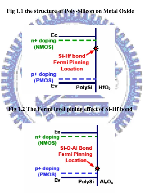
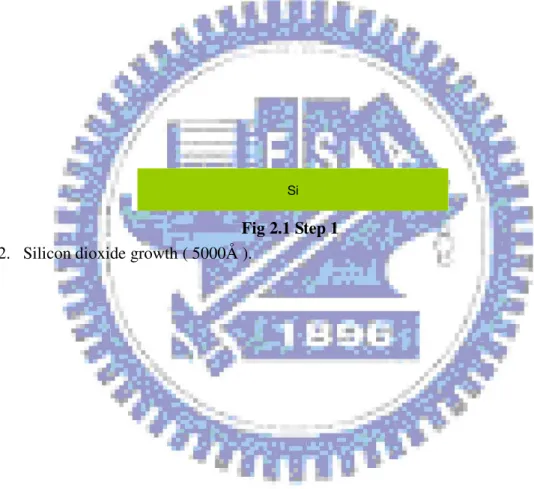
Poly-Silicon is conventional gate material for CMOS process, because of adjustable threshold voltage with different concentration of implantation. While the thickness of gate dielectric continue shrink, Poly-Silicon gate will face several problem. (1) the surface between Poly-Silicon and Metal oxide (high dielectric constant material, Fig 1.1)[26] will cause Fermi-Level Pinning Effect that causes high threshold voltage ( Fig 1.2-1.3 )[26]. (2) doped Poly-Silicon deprivation will cause larger parasitic capacitance. Base on the reason above, metal gate technology will be trend for CMOS process.
Metals which apply for CMOS process divide into two parts: 1.Middle Band-gap Metal: Ti Mo etc.
To use the same metal that can cause symmetry threshold voltage between NMOS and PMOS 2.Dual Metal System: NMOS: Al Ta TaN etc. (Low work function) PMOS: Au Pt etc. (High work function)
To use different metal which has different work function adjusts threshold voltage that matches the threshold voltage of NMOS and PMOS.
Fig 1.1 the structure of Poly-Silicon on Metal Oxide
Fig 1.2 The Fermi level pining effect of Si-Hf bond
1.6 Motivation
Although display technology does not suffer Fermi-Level Pinning Effect because of its thickness of gate dielectric film larger than 100nm, we still can adjust
drive current (ID) by using different metal which has different work-function. In this
thesis, we use Ytterbium (Yb, the Lanthanide series metal that previously gave
YbSi2-x low electron barrier to Si contact with good uniformity, work-function 2.6
eV) for gate material of NMOS, and will choose Iridium ( Ir work-function 5.27
eV) for PMOS in the future research. From the threshold voltage equation[27]:
NMOS: ms fp ox ox ss SD TN t Q Q V φ φ ε 2 ) | (max) (| ' − ' + + = PMOS: ms fn ox ox ss SD TP t Q Q V φ φ ε 2 ) | (max) | (− ' − ' + − =
The threshold voltage of NMOS decreases with lower φms, and the threshold voltage
of PMOS increases with higher φms, relatively, and we can get higher drive current.
We attempt to integrate this conception into Low Temperature Poly-Silicon technology that we can achieve high performance TFTs. In this thesis, we report
LaAlO3 gate dielectric with low work-function Ytterbium metal gate into LTPS TFTs
NMOS, which show a high breakdown voltage, low sub-threshold slope, high field-effect mobility, large on-off-state drive current ratio (Ion/Ioff) and high drive
current. The high breakdown voltage and high transistor drive current suggest that the
Ytterbium/LaAlO3 TFTs can meet the device requirements for both pixel and display
circuits. And then we hope that we can apply this technology for drive circuit on panel that realizes SOP ( System On Panel ).
1.7 Thesis Outline
In this thesis, we concentrate our efforts on metal gate for improving Poly-Silicon TFTs’ performance.
In chapter 1, a brief overview of Poly-Silicon TFTs technology was given to describe the various applications and characteristics of Poly-Silicon TFTs. And it also
shows our conception and motivation to use high –κgate dielectric and Ytterbium
metal gate.
In chapter 2, the fabrication process flows of low temperature Poly-Silicon TFTs
with metal gate and high –κ gate dielectric, experimental recipes and device
parameters extraction methods will be described.
In chapter 3, it shows the experimental data and the detail discussions of characteristics of high dielectric constant TFTs with metal gate includes high drive current, low threshold voltage, low sub-threshold slope, not bad mobility, and very good breakdown voltage. And it also shows the comparison between the performance of our conception and the performance of other TFTs’ design.
Finally, conclusions and future works as well as suggestion for further research are given in chapter 4.
Chapter 2
The Experimental Steps
2.1 The Fabrication Steps
Fabrication of the TFTs started with the formation of a Poly-Silicon film, by
depositing 100-nm amorphous Silicon on SiO2/Si wafers (using LPCVD at 550 oC),
followed by crystallization at 600oC and 20 hour annealing in N2. Then 500 nm thick
PECVD oxide was deposited for isolation and device active region was formed by patterning and etching the isolation oxide. The source and drain regions in the active
device region were implanted with phosphorus (35 KeV at 5×1015 cm-2) and activated
at 600oC for 12 hour annealing under N2. Then the 50 nm thick LaAlO3 gate dielectric
was deposited on previously patterned active region by sputtering from a LaAlO3
source with 150 W power and 30 sccm Ar flow rate. A 400oC and 30 min furnace O
2
treatment was applied to improve the gate oxide quality. Then gate was formed by depositing 200 nm Ytterbium using PVD. The TFTs devices were completed by gate definition with lift-off process, electrode formation and 400oC sintering for 30 min
under N2 ambient without using hydrogenation plasma passivation treatment. The
2.2 The Structure of fabrication
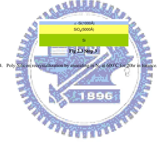
1. Silicon substrate.
Si
Fig 2.1 Step 1
2. Silicon dioxide growth ( 5000Å ).
Si SiO2(5000Å)
3. Amorphous Silicon deposition by LPCVD at 550˚C ( 1000 Å ).
Si SiO2(5000Å)
-Si(1000Å)
Fig 2.3 Step 3
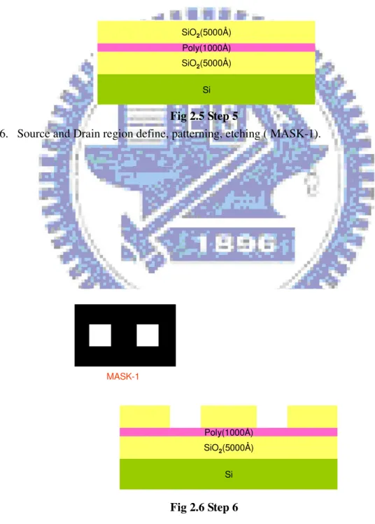
4. Poly-Silicon recrystallization by annealing in N2 at 600˚C for 20hr in furance.
Si SiO2(5000Å) Poly(1000Å)
5. Isolation oxide deposition by PECVD ( 5000 Å ) . Si SiO2(5000Å) Poly(1000Å) SiO2(5000Å) Fig 2.5 Step 5
6. Source and Drain region define, patterning, etching ( MASK-1).
Si SiO2(5000Å)
Poly(1000Å)
MASK-1
7. Source and Drain implantation with phosphorus ( 35KeV at 5e15 cm-2). Si SiO2(5000Å) Poly(1000Å) N+ N+ phosphorus Fig 2.7 Step 7 8. Activating in N2 at 600˚C for 12hr.
9. Removing Silicon on gate region ( MASK-2 ).
Si SiO2(5000Å) Poly(1000Å) N+ N+ MASK-2 Fig 2.8 Step 8 9
10.LaAlO3 deposition by PVD in Ar ( 150-W, 30-sccm, 500 Å ). Si SiO2(5000Å) Poly(1000Å) N+ LaAlO3(500Å) N+ Fig 2.9 Step 10
11.Contact hole define, patterning, etching ( MASK-3 ).
Si SiO2(5000Å) Poly(1000Å) N+ LaAlO3(500Å) N+ MASK-3 Fig 2.10 Step 11
12.Photoresist deposition Si SiO2(5000Å) Poly(1000Å) N+ LaAlO3(500Å) N+ PR Fig 2.11 Step 12
13.Metal region definition ( lift-off, MASK-4 )
Si SiO2(5000Å) Poly(1000Å) N+ LaAlO3(500Å) N+ PR PR MASK-4 Fig 2.12 Step 13
14.PVD-Yb deposition ( 2000 Å ) Si SiO2(5000Å) Poly(1000Å) N+ Yb(2000Å)LaAlO3(500Å) N+ PR PR Fig 2.13 Step 14 15.Removing PR Si SiO2(5000Å) Poly(1000Å) N+ Yb(2000Å)LaAlO3(500Å) N+ Fig 2.14 Step 15
Chapter 3
Result & Discussion
3.1 Method Of Device Parameter Extraction
In this thesis, we use Ellipsometer to measure the thickness of Poly-Silicon, amorphous-Si and dielectric films in the fabrication procedure. All the electrical characteristics of proposed Poly-Silicon TFTs were measured by HP 4156 Precision Semiconductor Parameter Analyzer. Many methods have been proposed to extract the characteristic parameters of Poly-Silicon TFTs. In this section, those methods are described.
3.1.1 Determination Of Threshold Voltage
Threshold voltage (Vth) is an important parameter required for the channel
length-width and series resistance measurements. However, Vth is not uniquely
defined. Various definitions have been proposed and the reason can be found in
ID-VGS curves. One of the most common techniques is the linear extrapolation method
with the drain current measured as a function of gate voltage at a low drain voltage of 50~100mV to ensure operation in the linear region [17]. The drain current is not zero
when VGS below threshold voltage and approaches zero asymptotically. Hence the IDS
extrapolated intercept of gate voltage (VGSi) by 2 DS GSi th V V V = − --- (Eq. 3.1)
Equation (3.1) is strictly only valid for negligible series resistance. Fortunately series resistance is usually negligible at the low drain current when threshold voltage
measurements are made. The IDS-VGS curve deviates from a straight line at gate
voltage below Vth due to sub-threshold current and above Vth due to series resistance
and mobility degradation effects. It is common practice to find the point of maximum
slope of the IDS-VGS curve (the same as the max-value point of Field Effect Mobility,
from Eq. 3.4)and fit a straight line to extrapolate to ID=0 by means of finding the point
of maximum of transconductance (Gm).
In other thesis, someone can use a simpler method to determinate the Vth called
constant drain current method. The voltage at a specified threshold drain current is
taken as the Vth. This method is adopted in the most studied papers of Poly-Silicon
TFTs. It can be given a threshold voltage close to that obtained by the complex linear
extrapolation method. Typically, the threshold current is specified at (W/L)×10nA for
VDS=0.1V and (W/L)×100nA for VDS=5V, where W and L are channel width and
channel length, respectively.
3.1.2 Determination Of Sub-threshold Slope
Sub-threshold slope (S.S.) is a typical parameter to describe the control ability of gate toward channel, which reflects the turn on/off speed of a device. It is defined as the amount of gate voltage required to increase/decrease drain current by one order of magnitude.
reality, the S.S. increases with drain voltage due to channel shortening effect such as charge sharing, avalanche multiplication and punchthrough effect. The sub-threshold slope is also related to gate voltage due to undesirable and inevitable factors such as the serial resistance and interface states.
In this thesis, the S.S. is defined as one-third of the gate voltage required to decrease the threshold current by three orders of magnitude. The threshold current is specified to be the drain current when the gate voltage is equal to threshold voltage.
3.1.3 Determination Of Field Effect Mobility
Usually, field effect mobility (µeff) is determined from the maximum value of
transconductance (Gm) at low drain bias. The transfer characteristics of Poly-Silicon TFTs are similar to those of conventional MOSFETs, so that the first order of I-V relation in the bulk Si MOSFETs can be applied to Poly-Silicon TFTs. The drain
current in linear region (VDS VGS Vth) can be approximated as the following
equation:
(
−)
− = 2 2 1 DS DS th GS ox eff DS L V V V V W C I µ --- (Eq. 3.2)where W and L are channel width and channel length, respectively. Cox is the gate
oxide capacitance per unit area and Vth is the threshold voltage. Thus, the
transconductance is given by DS ox eff GS DS m V L W C V I g = ∂ ∂ = µ --- (Eq. 3.3)
Therefore, the field-effect mobility is
(max) →0 = m VDS DS ox eff g WV C L µ --- (Eq.3.4)
3.1.4 Determination Of ON/OFF Current Ratio
On/Off current ratio is one of the most important parameters of Poly-Silicon TFTs since a high-performance device exhibits not only a large on-current but also a small off-current (leakage current). The leakage current mechanism in Poly-Silicon TFTs is not like that in MOSFET. In MOSFET, the channel is composed of single crystalline Si and the leakage current is due to the tunneling of minority carrier from drain region to accumulation layer located in channel region. However, in Poly-Silicon TFTs, the channel is composed of Poly-Silicon. A large amount of trap state densities in grain structure attribute a lot of defect states in energy band gap to enhance the tunneling effect. Therefore, the leakage current is much larger in Poly-Silicon TFTs than in MOSFET. When the voltage drops between gate voltage and drain voltage increases, the band gap width decreases and the tunneling effect becomes much more severe. Normally we can find this effect in typical Poly-Silicon
TFTs’ IDS-VGS characteristics where the magnitude of leakage current will reach a
minimum and then increase as the gate voltage decreases/increases for n/p-channel TFTs.
There are a lot of ways to specify the on and off-current. In this chapter, take n-channel Poly-Silicon TFTs for examples, the on-current is defined as the drain current when gate voltage at the maximum value and drain voltage is 0.1V. The off-current is specified as the minimum current when drain voltage equals to 0.1V.
V V at Plot V I of Current Minimum V V at Plot V I of Current Maximum I I DS GS DS DS GS DS OFF ON 1 . 0 1 . 0 = − = − = --- (Eq. 3.5)
3.2 Experimental Data Result & Discussion
The fabricated devices were characterized using HP4156 and HP4284 Precision Semiconductor Parameter Analyzer. We first show the data of NMOS-TFT (Yb /
LaAlO3). The Id-Vg characteristics of a representative TFT are shown in Fig. 3.1. The
threshold voltage is 0.85 V which is better than the threshold voltage of the device with aluminum gate which we reported before ( 1.2 V, Fig 3.2 ). The threshold voltage
decreases because that Ytterbium 2.6 eV) makes the lower φms. Base on the
threshold voltage equation: ms fp
ox ox ss SD TN t Q Q V φ φ ε 2 ) | (max) (| ' − ' + + = [27], lower ms
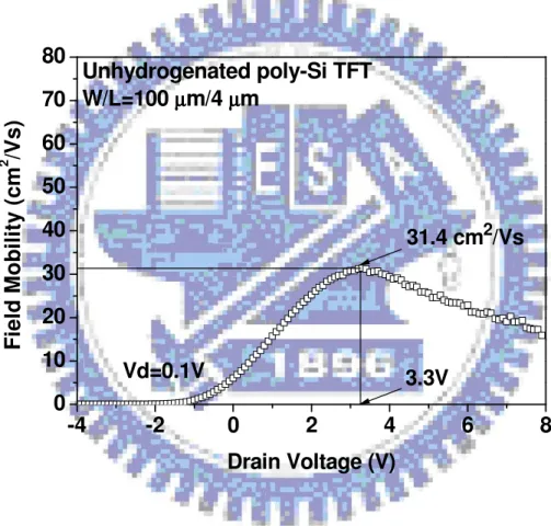
φ makes lower threshold voltage. And in Fig 3.3, we can see the sub-threshold
slope of 0.58 V/decade, the low sub-threshold swing indicates a low interface trap
density, and is consistent with the good electron field-effect mobility of 31.4 cm2/Vs
which is showed in Fig 3.4. This is because the sputtering and subsequent 400oC
oxidation also oxidized the poly-silicon surface. Although this is the undesired feature
in high κ CMOS to lower down the EOT [28-31], the good high-κ /Ytterbium
interface gives the not bad mobility and good sub-threshold slope. The Ion / Ioff ratio of
the Ytterbium/LaAlO3 TFT is 1.63×10⁶, even without performing hydrogen
passivation.
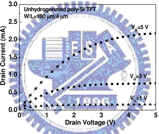
And then the output characteristics (Id-Vd) of the Ytterbium/LaAlO3 TFT are
high-speed display ICs. This good performance is related to the lower threshold
voltage and the high gate-capacitance of 3.9×10⁻⁷ F/cm2 from C-V measurements (Fig
3.6), which gives a small equivalent-oxide thickness (EOT) of 8.7 nm at a κ value
of ~22.5 [28][29] This is the thinnest reported EOT TFTs so far [32-35], And the high
drive current is higher than our past reported Al/LaAlO3 (EOT=8.7 nm) thin film
transistor, which is showed in Fig 3.7~3.13. It is because the work-function of Al
eV) is higher than that of Yb 2.6 eV). So the data affirm our conception. Our
design also provides an alternative way to create high drive current, along with existing approaches such as excimer-laser crystallization (ELC) [32][36-38], metal-induced lateral crystallization [39] and electric field enhanced crystallization [40]. It shows that good uniformity is also obtained due to the furnace crystallization, in contrast with the narrow process window and poor uniformity in ELC TFTs [41].
The field dependence of the gate current density is showed in Fig 3.14 shows a gate dielectric breakdown voltage of 31-32 V. This corresponds to an electric field of 6.25 MV/cm that is slightly larger than PECVD TEOS oxide of 5.4 MV/cm[35]. This is high enough to drive a liquid crystal display. This high breakdown field is comparable with or better than that for PECVD TEOS oxide [32-34][42]. This is important for achieving good dielectric reliability [28-31]. It may arise from the plasma-free process used, which does not damage the gate dielectric.
Figure 3.15 shows the charge-trapping characteristics of the Ytterbium/LaAlO3
TFTs under constant-current stress from 0.1 to 10 mA/cm2 (or ~2.9 to 5.8 MV/cm
electric field ). The gate voltage shift is only 0.61 V even under 10 mA/cm2 stress, which is much better than the 2.2 V shift in TEOS oxide TFTs under the same stress
condition [43]. Such low charge-trapping indicates the good quality of the gate
dielectric and is consistent with high – κLaAlO3 CMOSFETs also fabricated at low
temperature [28-29] and good intersurface between metal gate and high – gate
dielectric. Hence integrating high- κ gate dielectrics with Ytterbium metal gate into
TFT-NMOS should not degrade the TFT device reliability, often dominated by the
grain-boundary related hot-carrier degradation[44]
The important device parameters are summarized in Table 1, where the data from
devices using PVD LaAlO3 with Al gate, LPCVD SiO2 with poly-silicon gate,
PECVD TEOS oxides [33-35] with poly-silicon gate and Al2O3 gate dielectric with
Poly-SiGe gate [45]are also shown for comparison. The better device performance of
the Ytterbium/LaAlO3 TFTs that compared with LPCVD, PECVD TEOS oxide TFTs
(using the same furnace-crystallization process) and relative low –
κ
Al2O3 devices,is due to the lower threshold voltage which results from the higher capacitance
density combining with low work-function Ytterbium metal gate (Vth=
φ
ms +Gate
dielectric This work
LaAlO3 50 nm (8.7 nm EOT) LPCVD SiO2 80 nm[33] PECVD TEOS oxide 60 nm[34] PECVD TEOS oxide 40 nm[35] Al2O3 50 nm[45] Gate
electrode Ytterbium Aluminum Poly-Si Poly-Si Poly-Si Poly-SiGe
Vth (V) 0.85 1.2 5.6 8.14 Not extracted 3 FE (cm2/Vs) 31.4 40 20 12.44 3 47 Sub-threshold slope (V/decade) 0.58 0.31 1.4 1.97 2.67 0.44 Ion/Ioff 1.63×10⁶ 1.5×10⁶ 3.5×10⁵ 2.97×10⁵ Not extracted 3×10 5 Breakdown field (MV/cm) 6.25 6.3 Not extracted Not extracted 5.4 Not extracted Table 1
-2 -1 0 1 2 3 4 5 6 1.0x10⁻⁵ 2.0x10⁻⁵ 3.0x10⁻⁵ 4.0x10⁻⁵ 5.0x10⁻⁵ Unhydrogenated poly-Si TFT W/L=100 µµµµm/4 µµµµm D ra in C ur re nt (A ) Gate Voltage (V) 0.85V Yb Gate (Vd = 0.1V) 3.3V
Fig 3.1 The threshold voltage of Yb/LaAlO3 thin film transistor
-2 0 2 4 6 0.0 1.0x10⁻⁵ 2.0x10⁻⁵ 3.0x10⁻⁵ 4.0x10⁻⁵ 5.0x10⁻⁵ Unhydrogenated poly-Si TFT W/L=100 µµµµm/4 µµµµm D ra in C ur re nt (A ) Gate Voltage (V) Al Gate(Vd=0.1V) 3V 1.2V
Fig 3.2 The threshold voltage of Al/LaAlO3 thin film transistor
-4
-2
0
2
4
6
8
10
-1110
-910
-710
-510
-3D
ra
in
C
ur
re
nt
(A
)
Gate Voltage (V)
Unhydrogenated poly-Si TFT W/L=100 µµµµm/4 µµµµm Vd=0.1 Vsubthreshold slope=0.58 V/decade
-4
-2
0
2
4
6
8
0
10
20
30
40
50
60
70
80
Unhydrogenated poly-Si TFT
W/L=100
µµµµ
m/4
µµµµ
m
Fi
el
d
M
ob
ili
ty
(c
m
2/V
s)
Drain Voltage (V)
3.3V
31.4 cm
2/Vs
Vd=0.1V
0
1
2
3
4
5
0.0
0.5
1.0
1.5
2.0
2.5
3.0
V
G=5 V
V
G=3 V
D
ra
in
C
ur
re
nt
(m
A
)
Drain Voltage (V)
V
G=1 V
Unhydrogenated poly-Si TFT
W/L=100
µµµµm/4
µµµµm
-4
-3
-2
-1
0
1
0.00
0.05
0.10
0.15
0.20
0.25
0.30
0.35
0.40
C
ap
ac
ita
nc
e
(
µµµµ
F/
cm
2)
Bias (V)
LaAlO3 with 400oC 30 min O2 treatment
∆∆∆∆
V
hys=
< 70 mV
0 1 2 3 4 5 0.0 0.5 1.0 1.5 2.0 2.5 D ra in C ur re nt (m A ) Drain Voltage (V) Al(VG=1V)
Fig 3.7 The drain current of Al/LaAlO3 thin film transistor at Vg=1V
0 1 2 3 4 5 0.0 0.5 1.0 1.5 2.0 2.5 D ra in C ur re nt (m A ) Drain Voltage (V) Yb(VG=1V)
0 1 2 3 4 5 0.0 0.5 1.0 1.5 2.0 2.5 D ra in C ur re nt (m A ) Drain Voltage (V) Al(VG=3V)
Fig 3.9 The drain current of Al/LaAlO3 thin film transistor at Vg=3V
0 1 2 3 4 5 0.0 0.5 1.0 1.5 2.0 2.5 D ra in C ur re nt (m A ) Drain Voltage (V) Yb(VG=3V)
0 1 2 3 4 5 0.0 0.5 1.0 1.5 2.0 2.5 D ra in C ur re nt (m A ) Drain Voltage (V) Al(VG=5V)
Fig 3.11 The drain current of Al/LaAlO3 thin film transistor at Vg=5V
0
1
2
3
4
5
0.0
0.5
1.0
1.5
2.0
2.5
D ra in C ur re nt (m A ) Drain Voltage (V) Yb(VG=5V)0
1
2
3
4
5
0.0
0.5
1.0
1.5
2.0
2.5
D
ra
in
C
ur
re
nt
(m
A
)
Drain Voltage (V)
Yb(VG=1V) Al(VG=1V) Yb(VG=3V) Al(VG=3V) Yb(VG=5V) Al(VG=5V) Fig 3.13The comparison of drain current at different gate voltage between Yb-gate and Al-gate
0
1
2
3
4
5
6
7
8
10
-810
-710
-610
-510
-410
-310
-210
-110
00
5
10
15
20
25
30
35
40
Electric Field (MV/cm)
C
ur
re
nt
D
en
si
ty
(A
/c
m
2)
0
50
100
150
200
250
300
0.0
0.2
0.4
0.6
0.8
1.0
G
at
e
V
ol
ta
ge
s
hi
ft
(V
)
Stress Time (sec)
10 mA/cm
2stress
1 mA/cm
2stress
100
µµµµA/cm
2stress
4. Conclusion
We have fabricated and characterized high-performance LTPS TFTs-NMOS
which incorporate high- κ LaAlO3 dielectric with low work-function Ytterbium
metal gate that provides good dielectric properties such as a high breakdown field, low threshold voltage, low leakage current and low charge trapping rate. These devices exhibit excellent electrical characteristics and high drive current, even without special process steps. We can expect that we may achieve better performance by using hydrogenation passivation or excimer laser crystallization process steps to improve the trap density on interface or get high quality Poly-Silicon film. And we will keep the same conception on TFTs-PMOS by using higher work-function metal such as the second highest work-function metal, Iridium. We do not expect to use Pt (The highest work-function metal) because that it is difficult to be etched in process.. And finally, we may integrate this high performance device for drive circuit on panel that realizes SOP ( System On Panel ).
References
[1] T. Serilawa, S.shirai, A. Okamoto, and S. Suyama, “Low-temperature fabrication
of high-mobility Poly-Si TFTs for large-area LCD’s”, IEEE Trans. Electron Dev., vol. 36, no. 9, pp. 1929,1989.
[2] S. Ikeda et al., “Apolysilicon transistor technology for large capacity SRAMs”,
IEDM Tech. Dig., pp.469, 1990.
[3] F. Hayashi and M. Kitakata, “A high performance polysilicon TFT using RTA
and plasma hydrogenation applicable to highly stable SRAMs of 16 Mbit and beyond,” VLSI Technology, 1992. Digest of Technical Papers. 1992 Symposium on , 1992 , p36 –37
[4] S. Morozumi et al., “Completely integrated contact-type linear image sensor”,
IEEE Trans. Electron Dev., vol. 21, no. 8, p. 1546, 1985.
[5] Y. Hayashi et al., “A thermal printer head with CMOS thin-film transistors and
heating elements integrated on a chip”, ESSCC Digest, pp. 266, 1988.
[6] F. Okumura et al., in IDRC Digest, p. 174, 1988.
[7] N. Yamauchi, Y. Inaba, and M. Okamura, “An integrated photodetector amplifer
using -Si p-i-n photodiodes and poly-Si thin-film transistos,” IEEE Photonic Tec.
Lett., vol. 5, no. 3, p.319, 1993.
[8] H. C. Lin et al., “Deposition and Device application of in situ Boron doped
Polycrystalline SiGe Films Grown at Low Temperature”, J. Appl Phys. Lett., vol. 42, no. 9, pp. 835-837, 1993
[9] H. C. Tuan, “Amorphous silicon thin film and its applications to large-area
elements”, Mater. Rec. Soc. Ump. Proc., vol. 33, p247, 1984.
[11]M. G. Clark, “Current status and future prospects of Poly-Si devices,” IEEE
Proc.-Circuits Devices Syst., Vol. 141, No. 1, February 1994.
[12]A. Nakamura, F. Emoto, E. Fujii, and A. Tamamoto “A High-Reliablity,
Low-Operation-voltage Monolithic Active-Matrix LCD by Using Advanced Solid-Phase growth Technique,” IEDM Tech. P.847, 1990.
[13]N. Kubo, N. Kusumoto, T. Inushima, and S. Yamazaki, “Characterization of
polycrystalline-Si thin-film transistors fabricated by excimer laser annealing method.” IEEE Trans. Electron Devices, vol. 40, pp. 1876-1879, Oct. 1994.
[14]G. K. Giust and T. W. Sigmon, “Low-Temperature Polysilicon Thin-Film
Transistors Fabricated from Laser-Processed Sputtered-Silicon Films,” IEEE
Electron Device Lett., vol. 19, pp. 343-344, Sept. 1998.
[15]G. K. Giust and T. W. Sigmon, “High-Performance Laser-Processed Polysilicon
Thin-Film Tranasitor,” IEEE Electron Device Lett., vol. 20, no. 2, pp. 77-79, Feb. 1999.
[16]Zhiguo Meng, Mingxiang Wang, and Man Wong, Member, IEEE, “High
Performance Low Temperature Mateal-Induced Unilaterally Crystallized polycrystalline Silicon Thin Film transistors for System-on-Panel Applications,” IEEE Trans. Electron Devices, vol.47, no.2, Feb. 2000.
[17]Seok-Woon Lee, Tae-Hyung Ihn, and Seung-Ki Joo, “Fabrication of
High-Mobility P-Channel Poly-Si Thin Film Transistos by Self-Aligned Metal-Induced Lateral Crystallization,” IEEE Electron Device Lett., vol. 17, no.8 Aug. 1996.
[18]Won Kyu Kwak, Bong Rae Cho, Soo Young Yoon, Seong Jin Park, And Jin Jang,
“A High Performace Thin-Film Transistor Using a Low Temperature Poly-Si by Silicide Mediated Crystallization,” IEEE Electron Device Lett., vol. 21, no.3 March 2000.
[19]Eric Campo, Emmanuel Scheid, Danielle Bielle-Daspet, and Jean-Paul Guillemet, “Influence of Rapid Thermal and Low Temperature Processing on the Electrical Properties of Polysilicon Thin Film Transistos,” IEEE Trans. on Semi.
Manufacturing, vol. 8, no.3 Aug. 1995.
[20]Yong Woo Choi, Jeong o Lee, Tae Woong Jang, and Byung Tae Ahn, “Thin-Film
Transistors Fabricated with Poly-Si Films Crystallized at Low Temperature by Microwave Annealing,” IEEE Electron Device Lett., vol. 20, no. 1, pp. 2-4, Jan. 1999.
[21]I. W. Wu, T. Y. Huang, W. B. Jackson, A.G. Lewis, and A. Chiang, “Passivation
kinetics of two types of defects in polysilicon TFT by plasma hydrogenation,”
IEEE Electron Device Lett., vol. 12, no.4, p.181, 1991.
[22]T. I. Kamins, and P. J. Marcoux, “Hydrogenation of transistors fabricated in
polycrystalline-silicon films,” IEEE Electron Device Lett., vol. 1, no. 8, p.159, 1980.
[23]R. A. Ditizio, S. J. Fonash, and B. C. Hseih, “Examination of the optimization of
thin film transistor passivation with hydrogen electron cyclotron resonance plasma,” J. Vac. Sci. Technol. A, vo. 10, no. 1, p 59, 1992.
[24]M. Hack, A. G. Lewis, and I. W. Wu, “physical models for degradation effects in
polysilicon thin-film transistors,” IEEE Trans. Electron Devices, vol. 40, no. 5, p. 890, 1993.
[25]K. Nakazawa, “Recrystallization of amorphous silicon films deposited by
low-pressure chemical vapor deposition from Si2H6 gas,” J. Appl. Phys., vol. 60,
pp.1703-1706, 1991.
[26] C. Hobbs, L. Fonseca, V. Dhandapani, S. Samavedam, B. Taylor, J. Grant, L. Dip, D. Triyoso, R. Hegde,D. Gilmer, R. Garcia, D. Roan, L. Lovejoy, R. Rai, L.
Motorola, Austin, TX. Fermi Level Pinning at the PolySi/Metal Oxide Interface [27]Donald A. Neamen, ”Semiconductor Physics And Devices Basic
Principles. ”,Third Edition
[28] D. S. Yu, A. Chin, C. C. Laio, C. F. Lee, C. F. Cheng, W. J. Chen, C. Zhu, M.-F.
Li, S. P. McAlister, and D. L. Kwong, “3D GOI CMOSFETs with novel IrO2(Hf)
dual gates and high- κ dielectric on 1P6M-0.18 m-CMOS,” in IEDM Tech.
Dig., 2004, pp. 181-184.
[29] D. S. Yu, K. C. Chiang, C. F. Cheng, A. Chin, C. Zhu, M. F. Li, and Dim-Lee
Kwong, “Fully silicided NiSi:Hf/LaAlO3/smart-cut-Ge-on-insulator n-MOSFETs
with high electron mobility” IEEE Electron Device Lett. 25, pp. 559-561, Aug. 2004.
[30] C. H. Huang, M. Y. Yang, A. Chin, W. J. Chen, C. X. Zhu, B. J. Cho, M.-F. Li, and D. L. Kwong, “Very low defects and high performance Ge-on-insulator
p-MOSFETs with Al2O3 gate dielectrics,” in Symp. on VLSI Tech., 2003, pp.
119-120.
[31] A. Chin, Y. H. Wu, S. B. Chen, C. C. Liao, and W. J. Chen, “High quality La2O3
and Al2O3 gate dielectrics with equivalent oxide thickness 5-10Å,” in Symp. on
VLSI Tech. Dig., 2000, pp. 16-17.
[32] C. H. Tseng, T. K. Chang, F. T. Chu, J. M. Shieh, B. T. Dai, H. C. Cheng, and A. Chin, “Investigation of inductively coupled plasma gate oxide on low temperature polycrystalline-silicon thin film transistors,” IEEE Electron Device
Lett. 23, pp. 333-335, June 2002.
[33] Y. W. Choi, J. N. Lee, T. W. Jang, and B. T. Ahn, “Thin-film transistors fabricated with poly-Si films crystallized at low temperature by microwave annealing,” IEEE Electron Device Lett., vol. 20, pp. 2-4, Jan. 1999.
Lin, T. S. Chao, C. Y. Chang, “Effects of plasma treatments, substrate types, and
crystallization methods on performance and reliability of low temperature
polysilicon TFTs” in IEDM Tech. Dig., 1999, p. 305-308.
[35] K. M. Chang, W. C. Yang, and C. P. Tsai, ”Electrical characteristics of low temperature polysilicon TFT with a novel TEOS/oxynitride stack gate dielectric,” IEEE Electron Device Lett., vol. 24, pp. 512-514, Aug. 2003.
[36] G. K. Guist and T. W. Sigmon, “High-performance thin-film transistors fabricated using excimer laser processing and grain engineering,” IEEE Trans.
Electron Devices, vol. 45, pp. 925–932, April 1998.
[37] J.-H. Jeon, M.-C. Lee, K.-C. Park, S.-H. Jung, and M.-K. Han, “A new poly-Si TFT with selectively doped channel fabricated by novel excimer laser
annealing,” in IEDM Tech. Dig., 2000, pp. 213–216.
[38] C. H. Tseng, C. W. Lin, T. K. Chang, H. C. Cheng,and A. Chin, “Effects of
excimer laser dopant activation on the low temperature polysilicon thin-film transistors with lightly doped drains,” Electrochemical and Solid-state Letters, 4, p. G94-G97, Nov. 2001.
[39] S.-W. Lee and S.-K. Joo, “Low temperature poly-Si thin-film transistor fabrication by metal-induced lateral crystallization,” IEEE Electron Device Lett., vol. 17, pp. 160-162, April 1996.
[40] B. Kim, H.-Y. Kim, H.-S. Seo, S. K. Kim, and C. D. Kim, “Surface treatment effect on the poly-Si TFTs fabricated by electric field enhanced crystallization of Ni/a-Si:H films,” IEEE Electron Device Lett., vol. 24, pp. 733-735, Dec. 2003. [41] C. W. Lin, L. J. Cheng, Y. L. Lu, Y. S. Lee, and H. C. Cheng,
“High-performance low-temperature poly-Si TFTs crystallized by excimer laser irradiation with recessed-channel structure,” IEEE Electron Device Lett., vol. 22,
[42] C. A. Dimitriadis, P. Coxon, L. Dozsa, L. Papaddimitrious, and N. Economou, “Performance of thin film transistors on polysilicon films grown by LPCVD at various conditions,” IEEE Trans. Electron Devices, vol. 39, pp. 598–606, Mar. 1992.
[43] K. M. Chang, W. C. Yang, and B. F. Hung, ”High-performance RSD poly-Si
TFTs with a new ONO gate dielectric” IEEE Trans. Electron Devices, vol. 51,
pp. 995-1001, June 2003.
[44] T. Yoshida, K. Yoshino, M. Takei, A. Hara, N. Sasaki, and T. Tsuchiya, “Experimental evidence of grain-boundary related hot-carrier degradation mechanism in low-temperature poly-Si thin-film-transistors,” in IEDM Tech.
Dig., 2003, pp. 219–222.
[45] Z. Jin, H. S. Kwok, and M. Wong, “High-performance polycrystalline SiGe
thin-film transistors using Al2O3 gate insulators,” IEEE Electron Device Lett., vol.
Vita
Studies Of High Performance Metal Gate Low Temperature Poly-Silicon Thin Film Transistor.