IEEE ELECTRON DEVICE LETTERS, VOL. 27, NO. 4, APRIL 2006 291
A Micromachined CMOS Distributed Amplifier by
CMOS Compatible ICP Deep-Trench Technology
Tao Wang, Chun-Hao Chen, Yo-Sheng Lin, Senior Member, IEEE, and Shey-Shi Lu, Senior Member, IEEE
Abstract—A CMOS-process-compatible backside inductively coupled-plasma (ICP) dry etching technology to form deep trenches underneath the inductors of RF ICs is developed to enhance the performance of RF ICs with on-chip inductors. A 1–12.6-GHz CMOS distributed amplifier (DA) was designed and implemented in a standard CMOS process. The DA exhibits good input 1-dB compression point(P1 dB) of −2 dBm and input third
intercept point of 7 dBm both at 2.4 and 5.8 GHz. The authors demonstrate that a significant improvement in power gain(S21)
and noise figure (NF) can be achieved by conducting the proposed backside ICP dry etching to selectively remove the silicon under-neath the inductors of the DA. The result shows that a 1.06-dB increase inS21 (from 9.7 to 10.76 dB) and a 0.87-dB decrease
(from 5.51 to 4.64 dB) in NF are achieved at 5.8 GHz mainly due to the improvement of the quality factor of the inductors in the DA. This means that this backside ICP dry-etching technique is very promising for system-on-a-chip applications.
Index Terms—CMOS, distributed amplifier (DA), inductively coupled plasma (ICP), inductor, noise figure (NF), quality factor (Q), system-on-a-chip (SOC).
I. INTRODUCTION
R
ECENTLY, RF CMOS and BiCMOS processes have be-come more and more popular for RF ICs operated in the 5-GHz band [1] and even in the higher 30–100-GHz band [2]. However, the quality-factor (Q) performance of the monolithic RF inductors fabricated on normal silicon substrates, of which the thickness normally ranges from 280 to 750µm depending on the technology used [3], are not satisfactory up to now, mainly due to the losses in the conductive silicon substrate as well as the series resistance of the metallization. Various methods have been proposed to enhance Q, such as high-resistivity silicon [4], front side and backside micromachining [5], [6], porous silicon [7], proton implantation [8], and pat-terned ground shields (PGS) [9]. Only a few of these methods have verified their high-Q inductors in RF active circuits. This is because most of the proposed methods are very difficult, if not impossible, to be integrated into the standard CMOS technology due to their inherent nonstandard CMOS processing steps. In addition, the front side etching has inherent limitations such as how far the circuits can be placed from the inductors [5].Manuscript received January 4, 2006; revised February 7, 2006. This work was supported by the National Science Council (NSC) of Taiwan, R.O.C., under Contract NSC94-2215-E-002-032. The review of this letter was arranged by Editor C. Bulucea.
T. Wang, C.-H. Chen, and S.-S. Lu are with the Graduate Institute of Electronics Engineering and Department of Electrical Engineering, National Taiwan University, Taipei 10617, Taiwan, R.O.C. (e-mail: [email protected]).
Y.-S. Lin is with the Department of Electrical Engineering, National Chi-Nan University, Puli 54561, Taiwan, R.O.C.
Digital Object Identifier 10.1109/LED.2006.871857
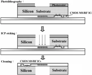
Fig. 1. Processing steps of the backside ICP deep-trench etching technology.
The PGS method, while compatible with CMOS technology, has the drawbacks of limited improvement ofQ and reduction of self-resonant frequency (fSR). Fortunately, these problems can be largely improved by our proposed CMOS-compatible IC postprocess, i.e., backside inductively coupled-plasma (ICP) dry etching technology.
In this paper, selective removal of the silicon underneath the inductors in RF ICs based on ICP deep-trench technology is demonstrated by a 1–12.6-GHz CMOS distributed amplifier (DA) fabricated on a 280-µm-thick silicon substrate. Satisfac-tory improvements in power gain(S21) and noise-figure (NF) performances are achieved.
II. DEEP-TRENCHTECHNOLOGY ANDDESIGN OFDA The processing steps of our backside ICP deep-trench tech-nology are shown in Fig. 1 and described as follows. First, for the ease of chip handling, the front side of the die(∼ 5 mm × 5 mm) with RF ICs was stuck to a glass substrate with adhesive S1813 followed by dropping photoresist SU8 on the backside of the sample. Note that these process steps can be omitted when applied in mass production because the wafer diameter is large. After standard photolithography processes on the backside of the die, the ICP dry etching was used to remove the silicon (280-µm thick) underneath the inductors. The main gases used during the ICP etching process were alternate SF6(for etching) and C4F8 (for passivation) with a 17-s cycle. The ICP etching rate being about 2 µm/min, the total etching time was about 140 min. Finally, the adhesive and photoresist, which covered the front side and backside of the die, respectively, was removed for test purposes. For the present small 5 mm× 5 mm chip, it
292 IEEE ELECTRON DEVICE LETTERS, VOL. 27, NO. 4, APRIL 2006
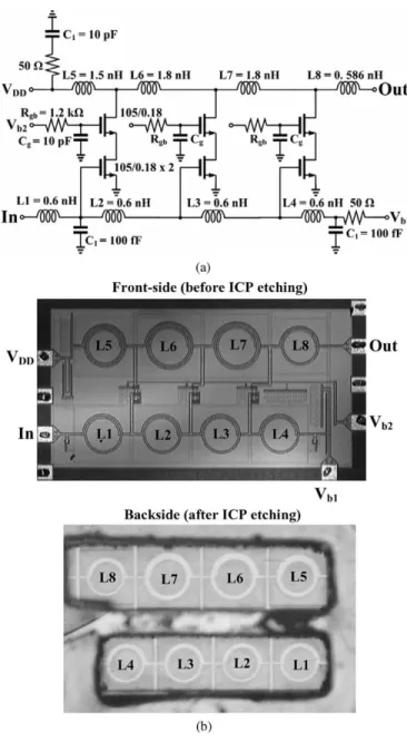
Fig. 2. (a) Schematic of the CMOS DA. (b) Front side (before the etching) and backside (after the etching) die photos of the CMOS DA. The DA occupies an area of 1.1 mm× 0.6 mm, excluding the test pads.
is found that the yield is 100% in the laboratory. It is not clear to us whether this process will be a low-cost and high-yield process in the industry. However, as technology advances, we believe that the yield of this process should also be high even for large-diameter wafers used in the industry.
Fig. 2(a) shows the schematic of the designed 1–12.6-GHz CMOS DA. Basic design guidelines for DAs can be found in [10] and [11]. Cascode field-effect transistors (FETs) were used to replace the traditional common-source FET to improve the gain performance. The damping resistorRgbin the gate of the common-gate transistor was used to improve the amplifier stability. Fig. 2(b) shows the front side (before the etching) and the backside (after the etching) die photos of the CMOS DA. As can be seen from the backside die photo, the exposed front side on-chip inductors are visible to the naked eye and the sidewalls of the “drilled” or micromachined holes are virtually vertical.
Fig. 3. Measured (a) power gain(S21) and input return loss (S11) and (b) NF and reverse isolation(S12) of the CMOS DA both before and after the backside
ICP dry etching.
Compared with the traditional backside wet bulk microma-chining, the dry ICP etching has the advantages of forming vertical sidewalls and being fully CMOS-process compatible, since it is a standard processing technique in modern CMOS technology.
III. MEASUREMENTRESULTS ANDDISCUSSIONS
The frequency-dependent S-parameter measurements were performed from 0.1 to 20 GHz by an HP-8510C network analyzer on several dice both before and after the backside ICP etching process. The supply voltage(VDD) and the power consumption (PDC) are 1.8 V and 39.6 mW, respectively. Fig. 3(a) shows the measured power gain(S21) and input return loss(S11) of the CMOS DA both before and after the backside ICP dry etching. As can be seen, the performance variation of
S21from die to die is obviously smaller than the improvement due to ICP. Even on a silicon substrate with high resistivity of 20 Ω · cm, a 1.06-dB increase in peak S21 (from 9.7 to 10.76 dB) is achieved at 5.8 GHz for the DA after the backside ICP dry etching. In addition, a significant improvement inS21 in the medium frequency range of 3–8 GHz is also achieved
WANG et al.: A MICROMACHINED CMOS DISTRIBUTED AMPLIFIER 293
for the DA after the backside ICP dry etching. For RF ICs fabricated with advanced RF-CMOS technologies, which nor-mally adopt low-resistivity silicon substrate(∼ 0.1 Ω · cm) for achieving tight n+–p+spacing, the effect of the backside ICP deep-trench technology would be more prominent.
Fig. 3(b) shows the measured NF and the reverse isolation (S12) of the CMOS DA both before and after the backside ICP dry etching. A 0.87-dB decrease (from 5.51 to 4.64 dB) in NF is achieved at 5.8 GHz for the DA after the backside ICP dry etching. In addition, a significant improvement in NF in the medium frequency range of 3–8 GHz is also achieved for the DA after the backside ICP dry etching. The reason why the measured NF for the DA with ICP inductors (ICP DA) is even worse than that of the DA with standard inductors (STD DA) at frequencies higher than 9 GHz can be explained as follows. In this paper, the ICP DA and the STD DA were both designed based on the standard inductors; that is, the same set of inductors was employed in the two experiments (STD DA and ICP DA). Although backside ICP dry etching can improve both the maximum Q (Qmax) and self-resonance frequency (fSR) performances of the inductors in the DA, the mismatch resulting from ICP etching becomes more prominent with the increase of frequency. At frequencies where the power gain loss resulting from the mismatch exceeds the power gain im-provement resulting from the imim-provement ofQ, the measured NF of the DA with ICP inductors becomes higher than that of the DA with standard inductors. This means that for RF ICs with operating frequencies higher than 8 GHz, in order to achieve significant improvements in both power gain and NF performances in all the frequencies of interest, the design of RF ICs should be optimized based on the ICP inductors and not on the standard inductors. That is, different inductors have to be used in the ICP and non-ICP design. A complete set of ICP inductors should be designed, fabricated, measured, and modeled [12]–[14]. In this way, an optimized design of ICP RF ICs can be achieved based on the created inductor models. Moreover, linearity performances of the DA have also been measured. GoodP1 dBof−2 dB and input third intercept point (IIP3) of 7 dB both at 2.4 and 5.8 GHz were achieved (not shown here).
IV. CONCLUSION
A CMOS-process-compatible backside ICP dry etching tech-nology to form deep trenches underneath the inductors of RF ICs was developed to enhance the performance of RF ICs with on-chip inductors. Significant improvements in S21 and NF were achieved for a test DA after the backside ICP dry etching. Apparently, the proposed ICP technology is also capable of
improving the isolation between RF/analog and digital circuits and thus paves a way for system-on-a-chip.
ACKNOWLEDGMENT
The authors are grateful for the support from the United Microelectronics Company (UMC) for integrated circuit fabri-cation under the UMC campus program, Chip Implementation Center (CIC) for chip fabrication, and National Nano Device Laboratories (NDL) for high frequency measurements.
REFERENCES
[1] H. W. Chiu, S. S. Lu, and Y. S. Lin, “A 2.17 dB NF, 5 GHz band monolithic CMOS LNA with 10 mW DC power consumption on a thin (20µm) substrate,” IEEE Trans. Microw. Theory Tech., vol. 53, no. 3, pp. 813– 824, Mar. 2005.
[2] T. O. Dickson, M. A. LaCroix, S. Boret, D. Gloria, R. Beekens, and S. P. Voinigescu, “30–100 GHz inductors and transformers for millimeter-wave (Bi)CMOS integrated circuits,” IEEE Trans. Microw. Theory Tech., vol. 53, no. 1, pp. 123–134, Jan. 2005.
[3] H. W. Chiu and S. S. Lu, “A 2.17 dB NF, 5 GHz band monolithic CMOS LNA with 10 mW DC power consumption,” in Symp. VLSI Tech. Dig., 2002, pp. 226–229.
[4] J. N. Burghartz, D. C. Edelstein, K. A. Jenkins, and Y. H. Kwark, “Spi-ral inductors and transmission lines in silicon technology using copper-damascene interconnects and low-loss substrates,” IEEE Trans. Microw.
Theory Tech., vol. 45, no. 10, pp. 1961–1968, Oct. 1997.
[5] H. Lakdawala, X. Zhu, H. Luo, S. Santhanam, L. R. Carley, and G. K. Fedder, “Micromachined high-Q inductors in a 0.18µm copper inter-connect low-k dielectric CMOS process,” IEEE J. Solid-State Circuits, vol. 37, no. 3, pp. 394–403, Mar. 2002.
[6] M. Ozgur, M. E. Zaghloul, and M. Gaitan, “Optimization of back-side micromachined CMOS inductors for RF applications,” in Proc.
IEEE Int. Symp. Circuits and System, Geneva, Switzerland, May 2000,
pp. V-185–V-188.
[7] H. S. Kim, D. Zheng, A. J. Becker, and Y. H. Xie, “Spiral inductors on Si p/p+ substrates with resonant frequency of 20 GHz,” IEEE Electron
Device Lett., vol. 22, no. 6, pp. 275–277, Jun. 2001.
[8] C. Y. Lee, T. S. Chen, C. H. Kao, J. D. S. Deng, C. C. Yen, Y. K. Lee, J. C. Kuo, J. F. Chang, G. W. Huang, K. M. Chen, and T. S. Duh, “A simple systematic procedure of Si-based spiral inductor design,” in Proc.
IEEE RFIC Conf., Jun. 2004, pp. 619–622.
[9] C. P. Yue and S. S. Wong, “On-chip spiral inductors with patterned ground shields for Si-based RF IC’s,” IEEE J. Solid-State Circuits, vol. 33, no. 5, pp. 743–752, May 1998.
[10] B. M. Ballweber, R. Gupta, and D. J. Allstot, “A fully integrated 0.5–5.5-GHz CMOS distributed amplifier,” IEEE J. Solid-State Circuits, vol. 35, no. 2, pp. 231–239, Feb. 2000.
[11] H. T. Ahn and D. J. Allstot, “A 0.5–8.5-GHz fully differential CMOS distributed amplifier,” IEEE J. Solid-State Circuits, vol. 37, no. 8, pp. 985– 993, Aug. 2002.
[12] A. C. Watson, D. Melendy, P. Francis, K. Hwang, and A. Weisshaar, “A comprehensive compact-modeling methodology for spiral inductors in silicon-based RFICs,” IEEE Trans. Microw. Theory Tech., vol. 52, no. 3, pp. 849–857, Mar. 2004.
[13] D. Melendy, P. Francis, C. Pichler, K. Hwang, G. Srinivasan, and A. Weisshaar, “Wide-band compact modeling of spiral inductors in RFICs,” in Proc. IEEE MTT-S Dig., 2002, pp. 717–720.
[14] Y. S. Lin, “Temperature and substrate-impedance dependence of noise figure of monolithic RF inductors on silicon,” IEEE Electron Device Lett., vol. 26, no. 6, pp. 397–400, Jun. 2005.