Low Leakage Reliability Characterization Methodology for
Advanced
CMOS with Gate Oxide in the
lnm
Range
Steve S. Chung’, H. J. Feng‘, Y. S. Hsieh*, Alex L i d , W. M. Linz, D. E Chen’, J. H. Ho’, K. T. Huang’, C. K . Yang’, Osben Chenp, Y. C. Sheng’, .D. Y. Wu’, W. T. Shiau’, S. C. Chien’, Kuan Liao’, and S. W. Sun’
‘ p e p y t m e ? t of Electronic Engineering, National Chiao Tung Universiry. Taiwan
United MIcmelectronics Corporation (UMC), Central R&D Division,, Taiwan
Abstract- A low leakage characterization technique for the lateral profiling of interface and oxide traps in a 12A-16A range gate oxide CMOS devices has heen demonstrated. The approach being taken includes an incremental frequency Charge- Pumping(1FCP) measurement and a neutralization procedure such that interface and oxide traps can be separated. The most critical steps are the elimination of leakage current during measurement and a neutralization procedure, which enables accurate determination of interface and oxide traps. This method has been demonstrated successfully for an advanced sub-l00nm CMOS devices. As an important merit for its application, evaluations of HC reliability and NBTI effect have also been demonstrated. Evaluations of gate oxide qualities with plasma nitridation in both n- and p-MOSFET reliabilities have been properly described based on the current analysis technique. 1. Introduction
There are three major techniqnes, i.e., charge pumping[l-2], gated-diode[3-41, and DCIV[S], for the characterization of interfaceloxide traps(Ni,/Q,,) in CMOS devices. However, for sub-100nm device with f, in the range 10-20A, as oftoday, none of the above has been provided for the quantitative calculation of Ni,/Q,,. A recent one reponed by the author using gated-diode for a thicker oxide is given in [6] where Nit and QOt can be separated. The gated-diode[3-41 and DCIV[5] can measure the generation- recombination current due to existing Neand/or Q., in the form of drain or substrate current, however, for very thin gate oxide, a
quantitative analysis is difficult and not available so far. In [ 7 ] , we have demonstrated successfully an IFCP(Incrementa1 Frequency Charge Pumping) method for the interface character- ization, in which a method has been developed to eliminate the leakage current error during the measurement. However, further effort is needed for a full characterization of device reliability, including hot carrier (HC) effect and Negative Bias Temperature Instability(NBT1) studies in particular for pMOSFET devices with bx5 20.4.
In this paper, a low leakage reliability evaluation technique has heen provided for the characterization of HC and NBTI effects, with focus on the profiling of interface/oxide traps. Results have heen demonstrated for more advanced technology with effective channel length (60nm) and ultra-thin (12-16A) gate oxide CMOS devices.
2. Device Preparation
The devices in this study were fabricated by the state-of-the-art IC manufacturing. 12-16A gate oxides CMOS devices were formed by advanced plasma nitridations and with several splits of nitride density (PNI-PN3). More detailed descriptions of these samples can also be found from [7].
3. Results and Discussion
A. Principle of the Low Leakage CP Method
Figure 1 shows the schematic diagram of a low leakage IFCP measurement developed by us previously in [7]. With both
S/D grounded and by applying a gate pulse with a fixed high level and a varying low voltage (Vg,), the channel will operate between accumulation and inversion. This ,gives rise to the charge pumping current IcP(=IS) measured from the bulk. Fig. I(b) shows the normal ( t 2 3 0 A ) and abnormal (b,<30A) CP curves, from which it can”he observed that when fX<30A, leakage occurs as a result of the tunneling between the gate and hulk. This will affect the calculation accuracy of the interface traps since interface trap is proportional to the value of measured ICP. Obviously, as revealed in Fig. 2, the leakage current increases largely with a reducing gate oxide thickness (e.g., V,, < OV for the ultra-thin oxide sample EOT= 12A).
Fig. 3 shows the steps of this IFCP method. We need to remove the leakage current during the CP measurement. Here, we use the approach by measuring CP currents at two different frequencies. For example, first, we measure the Icp at two different frequencies as in Fig. 3 , wherefi=2MHz andh=IMHz, from which we take the difference of
ICp
for these twofrequencies. This Icp becomes the lcp value at a new frequency fi- f2 = IMz. Table 1 lists the equations of this CP technique, in which a correct value of CP current is calculated by removing the leakage component by using two CP curves under different frequencies. Again in Fig. 4, it shows the linearity of the measured Icp with measurement frequency in that from the measured CP curves under various frequencies, the IC? for any frequency can he derived from a known frequency values. For example, Icp for lMHz is twice the value of that for SOOkHz, and is 5 times the value measured at 200kHz.
B. Lateral Profiling of InterfacdOxide Traps Along the Channel Direction
As is well known that the lateral profiling of the generated interface or oxide traps, needs to have two key element?., one is the charge pumping current and the other one is the so called local threshold voltage distribution, such that the distribution of traps can he delineated along the channel direction. In the past, several successful implementations of the method can he found from those reported in [I-21. Based on the hasic measurement of a device characteristics as shown in Fig. 5 , it shows the device drain currents of a fresh (hefore-stress, curve 1 ) and
a
stressed one(afier-stress, curve 2). For the presence of the interface and oxide traps, as can he seen from the measurement of GIDL current in Fig.6, we see that there are oxide traps generated in the gate oxide. Before calculating the profiling of either interface or oxide trap, we need to separate the contribution of charge pumping current contributed from both traps. As a consequence, to separate the Ni, from Qo,, the steps are as follows.I . First, for a fresh device, the drain current (at VG= -2V) is measured, curve (I). Again, the device is stressed and its current, curve(2), is measured, Fig. 5 .
To identify whether Qo,is generated, we monitor the GIDL current as given in Fig. 6, from which we see a shift between curve(1) and curve(2) corresponding to a threshold voltage shift, VT, caused by the Qat. A neutralization is performed in three-step, in which curve(2) is moved to curve(3) and then aligned with the fresh one, curve(1). Specifically, first, we inject negative charges into the gate 2.
19.2.1
oxide from the gate edge (Vo= OSV, Vn= -2V. time= Ssec).
Second, we inject negative charges by FN tunneling under the gate channel (V@ 2.W. time=5sec). Finally, we use the bias condition (Vo= 0.5, Vo=VB= -ZV, t i m e 30sec) to eliminate the hole traps completely. In Fig. 6. we s e e the GIDL shifts back to the fresh state.
At the same time, Icp, are measured as shown in Fig. 7, the difference between curves ( I ) and (3) gives the AIcp. In accordance with Eq. ( 2 ) in Table 11, we calculate the value of dAI,,IdV,, and dV,,ldx to obtain the lateral distribution of N,(x). Here, dV,,(x)/dx or dVT(x)/dx can he obtained in a similar way as those described in [ 2 ] . On the other hand, the difference between curves ( 2 ) and (3) give the Qdx) by using Eq. (4) in Table 11. The calculation of N;, and QOt is thus completed.
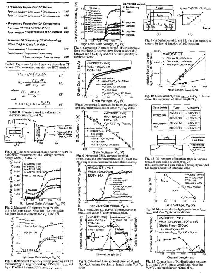
Results of the N;, and No,(= QJq) distributions are shown in Fig. 8, in which the drain junction is located at AI&=
O.OZpm(Fig. IO). The method to determine the physical lateral junction of source or drain with the body can be found in [7] (also in Fig. 9) and the results for the total N..s are shown in Fig. IO. These results indicate that the device with higher nitrogenation contents exhibits a larger slope and hence a larger amount of N.. Besides, from the calculated value for several different test samples in Fig. 11, it reveals that the one with additional RPN treatment has a larger amount of interface traps. C. Applications to Evaluating Device HC Reliability
3.
To evaluate the HC reliability, in Fig. 12, we measure the I, degradation of nMOSFET device after Iomx (V, O.5V, Vo= ZV), IB.MI.(VG= 1.4V. Vn= 2V), and VF Vo
( V e
Vn= 2V) stress conditions, respectively. The maximum In degradation is found at V e Vn stress condition. Figs. 12 and 13 show the consistency that V,=VD stress exhibits a largest 1, degradation and larger Ni distribution comparing to those of Ie.mr stress.As an application of the profiling of interfaceloxide traps, it can be used to identify the quality of gate oxide using different dosages of nitrogen. Fig. 14 shows the comparison of the oxide quality between the PNI and the PN3 with the same gate oxide thickness (EOT= I&). We observed the PNI sample is worse than PN3 sample after VG VD= 2V stress. AS shown in this figure, the N.(x) of PNI sample is larger than that of PN3 sample whether in the gate channel or in the overlap region. Here, we see that a higher concentration of plasma nitridation is better to resist the channel hot elemon injection since PN3 sample reliability has been improved with a high plasma density and N2 content close to the poly-SiOzinterface. In other words, higher concentration of plasma nitridation has better HC stress
reliability for nMOSFET.
TO study the dependency of the HC reliability on the gate oxide thickness. we found that a thicker sample has worse reliability after the stress. l l i s result is consistent with lateral profiling for two different gate oxide thickness samples as in Fig.
15. The thicker sample ( I d ) has larger area of Nu than thinner .
sample (14A) so that it has worse hot carrier reliability. We think the Ni, at p-substrate of a fiesh device is donor type interface trap, so above the quasi-Fermi level E@, the pOhrity of N. is positive. Since a thinner sample ( 14A) has smaller Nh than thicker sample (16A) ones for a fresh device, the N;, of thinner sample (14A) provides less attractive force to channel hot electron injection and hence induced less Nu after the stress. Based on this reasoning, we believe that the N;, of a fresh device will affect the amount of hot electron injection for nMOSFET device.
In a similar manner, experiments have been performed for pMOSFET, in which a pulse with high state V,, keeping fixed and with a varying pulse low voltage V,, applied at the gate, the charge pumping current can be measured as shown in Fig. 16.
19.
The experimental steps to d o the neutralization for pMOSFET are shown in Fig. 17 and the profiling results for
N ,
andNo,
are given in Fig. 18. Similar results for the drain currentdegradation shown in Fig. 19 reveals that the largest degradation occurs at Vo= Vo stress condition. Using the same approach as that in nMOSFET to separate N,, and Q,,, we have the lateral profiling of interface traps Nl(x) and oxide traps Q.,(x), as shown in Figs. 20 and 21 for different N2 contents and different gate oxide thickness, respectively. Here, it was noted that the PN3 sample is worse than PNI sample after Vo= VD= -2V stress. This might he due to an acceptor type interface trap at the n-substrate and if the interface traps are under the quasi-Fermi level Eh, the polarity of Na is negative which can attract hot hole injection. Since PN3 has larger amount of N2. it creates larger attractive force for hot hole injection during stress and then leads to more generation of N;,.D. Applicatiom to pMOSFET NBTI Studies
To explore further merit of the present approach, NBTI induced degradations were studied. There are two different modes of NBTI. For symmetrical NBTI, a negative bias is applied at the gate while S / D and substrate are grounded. Fig. 23 shows the profiling results of
N.
at 1M)"C. For asymmetrical NBTI, V p V n stress is applied at 100°C. The measured Io and GIDL currents and the procedures similar to Fig. 17 should he made. From the results of both Figs. 23 and 24, we can see that N. is largely enhanced on the drain side, which is attributed to a combination of NBTI and HC effect [3]. As a final verification of NBTI, both samples were subject to asymmetrical stress and with profiling results given in Fig. 25, where PN3 with high density plasma nihidation exhibits a largest Nu as a result of larger N2 content and its interaction with H2.As a conclusion of the observed NBTI effects: (I) the symmetrical NBTI effect will generate a double hump(Ni,) at the
S / D junction region(Fig. 23). (2) Nit is greatly enhanced for device under asymmetrical NBTI stress. where both
HC
and pureNBTI
effect can b e seen at the drain side(Fig. 24), and (3) larger amount of Na has been generated in a heavily nitrided pMOSFET as shown in Fig. 25.In summary. the low leakage CP measurement (IFCP). equipped with a neutralization step, has been demonstrated successfully for the interface characterization of ultra-thin gate oxide devices. It allows fast determination of both Ni, and Qm generated under both HC and NBTI stresses. In particular, the quantitative profiling of Ni,/Qo, is the first one reponed io dare
for b.c2O A devices. Evaluation of gate oxide qualities with plasma nitridation in both n- and p-MOSFET reliab
been adequately described based on the current analysis tech- nique. Results have shown that the present profiling technique has been a useful approach toward an understanding of the device HC reliability and NBTI effects for CMOS devices with different techniques of nitridation and with ultra-thin gate oxide thickness.
Acknowledgments This work was supported in pan by the Natioml Science Council, lhiwan, under contract NSC91-2215.E009-040. References
[I1 S. S . Chung et al..Pmc. SSDM,pp. 8 4 3 4 3 , 1993.
[2] C.ChenetaL.IEEET-ED..Vol.45, No. Z.pp.512-519. 1998. [3] S. S . Chung et al., in Tech. Dig. IEDM, pp. 513-516.2002, 141 S. -J. Chen et al., Proceedings of IRPS, pp. 203-207.2003.
151 C. T. Sah. Proceedings of 6th ICSICT. pp. 1-15,2001.
[6] S. S. Chung et al.. Symposium on V U 1 Tech, pp. 19-20. 1997. [7] S. S. Chung et al.. Symposium on VLSI Tech, pp. 19-20.2002.
.2.2
b " R -U 7 ICW, -U - lsnn -I berween the ? f = f j -f2. and can be multiplied by an
6
J
71vm.MM,,
.
Icw,.nn,,.*m, 3(bJ algebraic factor. 3sand
(4)
A', ( x ) = Q, ( r ) / q =
c,?v,
nMOSFET
.
PNI ( , O W N . , EO,= 141,Table I1 Equations used to calculate the dirvlbutions of N,< and N,.
".,CPC""
,..C. 6. L IOA
.,..(I,*
,...
I C I--C " A
Fig. I (a) Thhc schematic of charge pumping (CP) for nMOSFET measurement. (b) Leakage cumnts occurs when f,' ZOA. 171
I
0.0 0.5 1.0
0 High Level Gate Voltage, Vnh (V)
w , , Fig. 2 Measured CP cments for ulua thin
(12-16A) gate oxide. Note that IZA gale oxide
"
High Level Gale Voltage, V,, (V) Fig. 3 Incremental frequency charge pumping (IFCP)
methodology- using two-~eakage
cr
curves, kp,, andLn.
Lo obtain a c o m e t CP curve, kp,,,_,,
~ n _Channel Lenglh (pm)
Fig. 8 Calculated Lateral distribution of N,, and
No,(=Qa/q) along the channel length under Vo= V,
S W S S .
Mask Length, bsK (irm)
Fig. 10 Calculated N,, from &p,MAx in Fig. 1. It also s h o w the cxmcfion of offset length ?Lo
... .~
.
R*l.ldl*edB a s mid*
P - l
\:""
n trap.U \ ...
Fig. 11 (a) Amount of interface maps in vaious types of gate oxide devices (Fig. 2).
(b) Plasma nitrided gate oxide. The highly nitnded has larger amount of inlerface vaps.
Gale Voltage, VQ (V) Fig. 12 Measured device I, degradation at L,=-,
1.
-..,
and V,= V, - .suess conditions.nMOSFET(PN1)
-U W/L= 10/0.09pm, EOT= 14A
k 1
Stress Time= 250secI
Channel Length (pm)
Fig. 13 Comparison of N,, distribution between
lB, and V,= VD suess conditions. Note that V,= V, has much lager values of NLr
19.2.3
Channel Length (p)
Fig. 14 Comparison of the generated N,, for ~ W O different plasma nitrided samples, where PN3 reliability has been improved with a high plasma density and N,content close to oolv-Si.
Channel Length (pm)
Fig. 15 Comparison of the generated N, for two different gate oxide thicknesses, where thinner oxide shows better reliahilifv
pMOSFET (PNl) WIL= 1010.09 pm Slress@V,= 2V
.
- . v B = v o - ~ \ 0 0 0 5 1 0 $ 5 2 0 2 1 Gate Voltage, VG (V)Fig. 19 (pMOSFET1 Measured device I, degradation
at I,,,, IBW, and VG= V D stress conditions. Fig. N,, for two different gate oxide thicknesses. where 21 (pMOSFET) Comparison of the generated thinner oxide shows better reliability.
Fig. 22 Calculated N from I,,., in Fig. 16. It also shows the exv&on of offset length ? b.
Drain V d I w , V, Gate Voltage. V, (9
Fig. 17 (Left) Drain cumenis for fresh, Stressed, and after
neutralization. N is dominant from these cuwes. (Right)
The neutralizari& procedure is similar to fig. 5
Channel Length (rm)
Fig. 18 Calculated Lateral drsvibution of N,, and N,(=QJq) along the channel length under V,= V,
shess for pMOSFET device.
Fig. 23 Symmeeicai NBTI smis where D and S are
grounded and Vo= -2V. stressed ai T= IOWC. N,, distribution with double-hump can be seen at the
S D side.
- 8
2
~MOSFET (PNI) reliability.Fig. 25 Asymetrical NET1 &es.es~ where source is grounded while V,= Vn= -2V is applied at the drain side. Note that PNI hnr a lower plasma nibidation density and a better
0
'
Stress@VG=Vo=-2V j $ Time=25Osec-
4 2m
'
-.-
lnierlace Trap c B c sourcc;
-
$ ti$
2 -0-OIideTrap 2 0 Temp.=lOO"C+
-
0 0.03 0 03 0.06 0.09 Channel Length (pm)Fig. 24 Asymmetrical NBTI smss where source is grounded
while V,= V,= -2V is applied at the drain side. Note that N,, is dominant of the device degradation since N.. has l m ~ e r vzilues inride the channel region