國立交通大學
光電系統研究所
碩士論文
微波退火技術應用於新穎式透明非晶態銦鎵鋅氧薄膜電晶體
之研究
Study of Microwave annealing Technology on Novel
Transparent Amorphous Indium Gallium Zinc Oxide Thin
Film Transistors
研 究 生 : 羅婉柔 Yuan-Jou Lo
指導教授 : 劉柏村 教授 Prof. Po-Tsun Liu
林建中 教授 Prof. Chien-Chung Lin
微波退火技術應用於新穎式透明非晶態銦鎵鋅氧薄膜電晶體之研究
Study of Microwave Annealing Technology on Novel Transparent
Amorphous Indium Gallium Zinc Oxide Thin Film Transistors
研 究 生 : 羅婉柔 Yuan-Jou Lo
指導教授 : 劉柏村 教授 Prof. Po-Tsun Liu
林建中 教授 Prof. Chien-Chung Lin
國立交通大學
光電系統研究所
碩士論文
A Thesis
Submitted to Institute of Photonic System College of Photonics
National Chiao Tung University in partial Fulfillment of the Requirements
for the Degree of Master
in
Photonic System
October 2012
Hsinchu, Taiwan, Republic of China
微波退火技術應用於新穎式透明非晶態銦鎵鋅氧薄膜電晶體
之研究
研究生: 羅婉柔
指導教授: 劉 柏 村 教授
林 建 中 教授
國 立 交 通 大 學
光電系統研究所
摘 要
非晶態氧化半導體(Amorphous Oxide Semiconductors: AOSs) 具有高載子遷移
率而且可低溫沉積、可撓曲、透明性以及均勻度佳等特點已受到廣泛的重視。目
前被研究的氧化半導體有 ITO、IZO、TiO2
、ZnO、In2
O
3、Ga2
O
3、IGO、a-IGZO…
等。其中以透明非晶態氧化銦鎵鋅(Amorphous InGaZnO: a-IGZO)薄膜當作主動層
(Active layer)的薄膜電晶體(Thin Film Transistors: TFTs),具有載子遷移率與可靠
度比傳統氫化非晶矽薄膜電晶體(a-Si:H TFT)高、均勻性優於低溫複晶矽薄膜電晶
體(Low Temperature Polycrystalline Silicon TFT: LTPS TFT) 而且可低溫製程,因
此 a-IGZO 薄膜電晶體具有取代氫化非晶矽薄膜電晶體與低溫複晶矽薄膜電晶體
來製作主動矩陣有機發光顯示器(Active Matrix Organic Light Emitting Display:
AMOLED)的潛力。但是 a-IGZO 存在著一些本質上的缺點,例如對光以及環境中
的水、氧很敏感進而影響元件的穩定性。然而,a-IGZO TFT 長時間操作的可靠度
也是需要探討。本論文主要研究 a-IGZO 經由微波退火後的穩定性分析、元件長
時間操作的可靠度分析與紫外光影響元件穩定性分析等三個主要方向來進行探
討,以期得到改善元件穩定性的方法。從實驗結果我發現,當增加微波退火時間
和能量,可以提升元件穩定性與可靠度。以這個特性,最後我提出新穎式微波退
火技術以改善傳統爐管退火長時間以及高溫的特性。
Study of Microwave Annealing Technology on Novel
Transparent Amorphous Indium Gallium Zinc Oxide Thin
Film Transistors
Student : Yuan-Jou Lo
Advisors : Prof. Po-Tsun Liu
Prof. Chien-Chung Lin
College of Photonics & Institute of Photonic System
National Chiao Tung University, Hsinchu, Taiwan
Abstract
Amorphous oxide semiconductors (AOSs) are attracted much attention due to
high mobility, low temperature deposition, flexible,transmission, and uniformity.It
has been investigated of AOSs, such as ITO, IZO, TiO
2, ZnO, In
2O
3, Ga
2O
3, IGO,
a-IGZO,etc. Especially,the thin film transistors (TFTs) with a-IGZO thin film as
active layer perform higher mobility and better reliability than conventional
hydrogenated amorphous silicon TFT (a-Si: H TFT). In addition, the uniformity of
a-IGZO TFT is also superior to Low Temperature Polycrystalline Silicon TFT
(LTPS TFT). Therefore, the a-IGZO TFTs have the potential to replace a-Si: H TFT
and LTPS TFT forming Active Matrix Organic Light Emitting Display (AMOLED).
However, a-IGZO there are some inherent defect, such as sensitive to water and
oxygen in ambient and light illumination thereby affect the device stability. The
device reliability under GBS also has to be considered.In this thesis, we studied the
interaction between microwave annealing and furnace annealing a-IGZO thin film
transistors.Time dependence threshold voltage variation reliability are investigated.
Photo-reaction of a-IGZO TFT under UV-illumination is also investigated. From
the experimental results, increasing microwave annealing time and power can
improve the device stability and reliability under GBS. Finally we successfully
investigated that microwave annealing can get better electrical characteristics,
stability and reliability than furnace annealing.
誌謝
首先要感謝我的指導教授劉柏村教授為我們建立了一個資源豐富的研
究環境,讓我的碩士班生涯裡受益良多!無論在求學和生活中,老師都給予了
我最無私的指導與關懷。除了設備完善讓我們可以有世界級的研究成果,高水
準的的師資與研究團隊可以隨時與世界頂尖研究成果爭雄,成為更全方位的人
才,可以在未來為校爭光,回饋培育我們的社會。
在實驗的過程中首先要非常感謝鄧立峯與傅治翔學長,一直帶領我們
學弟妹,也不時給我們關心並給予指點並有情有義的帶著我們畢業。還要感謝
我的兩位夥伴王薇雅與張智翔,與我在無塵室內的量測機台共度無數時光。在
漫漫長夜也有破曉時分,擁有得來不易的令人欣慰的成果時,喜悅可以彼此共
享。同時也感謝實驗室中一起成長的好夥伴們揚順、光廷、震碩、立煒學長以
及亦君、俊彥、沁卉等這兩年以來的互相扶持與鼓勵,陪伴我度過這每一刻研
究生涯。還有豐榮、玫諍與韋勳等的加入也使實驗室注入了新的活力。一起相
約打球、聚餐或出遊玩樂等無數歡樂時光也將是珍貴而不可取代的美好回憶。
最後,我要感謝我的父母家人,你們的養育之恩、栽培之情與不離不
棄的陪伴,比任何言語都要深刻而有力的支持著我,讓我能夠繼續堅定地朝著
理想而前進。我會用一切的努力來報答,並用這篇論文獻給我最愛的家人。
Chinese Abstract………..………...I
English Abstract………....…..II
Acknowledgements…………...……….….III
Contents………...IV
Figure Captions...……….……....……..……....VI
Table Captions...VIII
Contents
Chapter 1 Introduction
1.1.
General Background
………...……..…...11.2.
Amorphous Oxide Semiconductors
………..…..……41.2.1. Introduction to Amorphous Oxide Semiconductor………….……….4
1.2.2. The Carrier Transport Mechanism of AOSs……….………...7
1.2.3. Amorphous IGZO………..……...9
1.3. Microwave Annealing Process
………..………..…...…...141.3.1. Interaction of Microwaves with Matter...14
1.3.2. Microwave Processing of Materials……….………….……...…..……18
1.4. Thesis Organization
.………...…...20Chapter 2 Experiment Procedures
2.1. Experiment Procedures
………...………...…………...212.3. Basic Microwave Heating System
………...262.4. Parameter Extraction Method
……….………...282.5. Measurement of Reliability on a-IGZO TFTs………..….
30Chapter 3 Results and Discussion
3-1. The effect of different MWA time on a-IGZO TFT
………...…...313.1.1. a-IGZO TFT with SiO2 gate insulator………...31
3.1.2. a-IGZO TFT with SiNx gate insulator……….…...33
3-2. The effect of different MWA Power on a-IGZO TFT
……….…………...353.2.1. a-IGZO TFT with SiO2 gate insulator……….…….…...35
3.2.2. a-IGZO TFT with SiNx gate insulator……….……….…...37
3-3. The comparison of MWA and Furnace annealing on a-IGZO TFT
...393.3.1. a-IGZO TFT with SiO2 gate insulator……….…..39
3.3.2. a-IGZO TFT with SiNx gate insulator………..….41
3-4. Material Analysis Results
……….……43Chapter 4 Experimental Results and Discussion
4-1. Conclusions
……….….48Figure Caption
Fig. 1-1 The basic operation of the pixel array: After the scan line was selected,
the data line applied a voltage to charge the storage capacitor…………....
2Fig. 1-2 Cross section of a LCD’s subpixel………..………...
3Fig. 1-3 Schematic orbital drawing of electron pathway (conduction band bottom)
in
conventional
silicon-based
semiconductor
and
ionic
oxide
semiconductor………...………...
7Fig. 1-4 Transmittance of a-IGZO film in visible light region...
10Fig. 1-5 The carrier concentration as a function of O
2pressure during the deposition
in a- InGaZnO
4and a-In
2Zn
3O
6...
12Fig.
1-6
(a)
The microwave heating system, (b)
the setup in the microwave
chamber.………...
20Fig. 2-1 The cross-section of a-IGZO TFTs...
24Fig. 2-2 Schematic DC sputtering system………...
26Fig.
3-1
The
electrical
characteristics
of
different
MWA
time
for
SiO
2gate
insulator. …..………..…………..……..
31Fig.
3-2
The
PBIS
and
NBIS
results
for
different
MWA
time
for
SiO
2gate
insulator..………...
32Fig.
3-3
The
electrical
characteristics
of
different
MWA
time
for
SiN
xgate
insulator………...
33Fig.
3-4
The
PBIS
and
NBIS
results
for
different
MWA
time
for
SiN
xgate
insulator………...
34Fig.
3-5
The
electrical
characteristics
of
different
MWA
power
for
SiO
2gate
insulator………..…………....
35Fig.
3-6
The
PBIS
and
NBIS
results
for
different
MWA
power
for
SiO
2gate
insulator………...
36Fig.
3-7
The
electrical
characteristics
of
different
MWA
power
for
SiN
xgate
Fig.
3-8
The
PBIS
and
NBIS
results
for
different
MWA
power
for
SiN
xgate
insulator………..………...
38Fig. 3-9 Electrical characteristics comparison with MWA and furnace annealing for
SiO
2gate insulator………...
39Fig. 3-10 The PBIS and NBIS comparison of MWA and furnace annealing for SiO
2gate insulator………...
40Fig. 3-11 Electrical characteristics comparison with MWA and furnace annealing
for SiN
xgate insulator……….
41Fig. 3-12 The PBIS and NBIS comparison of MWA and furnace annealing for SiN
xgate insulator………...
42Fig. 3-13 The X-ray diffraction results for different MWA time, MWA power and
furnace annealing…...……….……....
44Fig. 3-14 The scanning electron microscope results for different MWA time, MWA
power and furnace annealing………...……...
45Fig. 3-15 The X-ray photoelectron spectroscopy results for different MWA time,
MWA power and furnace annealing……….…..
46Fig. 3-16 The X-ray photoelectron spectroscopy results of 2P_100s and furnace
Table Caption
Table 1-1 The comparison of a-Si TFT, poly-Si TFT and TAOSs TFT………
4Table 2-1 Experiment flow chart………..……
24Table 2-2 The experiment flow of devices under light illumination………....
30Table 3-1 The data of MWA different time for SiO
2gate insulator………...
32Table 3-2 The data of different MWA time for SiN
xgate insulator………...
33Table 3-3 The data of MWA different power for SiO
2gate insulator………….….
36Table 3-4 The data of different MWA power for SiN
xgate insulator………….….
37Table 3-5 The data of comparison with MWA and furnace annealing for SiO
2gate
insulator………...…...
40Table 3-6 The data of comparison with MWA and furnace annealing for SiN
xgate
insulator………...
42Table 3-7 The data of optical band-gap for different MWA time, MWA power and
furnace annealing………..………...………...
43Chapter 1 Introduction
1.1 General background
Display is the widely used productions. We can find a lot of applications in our daily life.
Therefore, display technologies become more and more important in recent years. Display
industry can be considered to start from cathode ray tubes and transfer to TFTs. In this case,
we need the brief introduction about TFT-LCD. The basic structure of a TFT-LCD panel, as
shown in Fig. 1-1 [1], may be thought of as two glass substrates sandwiching a layer of liquid
crystal. The upper glass substrate is fitted with a color filter, while the back glass substrate has
transistors fabricated on it. Furthermore, the black matrix, an opaque polymer, which is
deposited on the upper glass structure, blocks the environment light to illuminate the front of
TFT and incidentally avoids the incorrect color mixture by back light through color filter. [2]
As shown in Fig. 1-2 [2] we can see the cross-section of TFT-LCD’s subpixel. However,
nothing shields the light from back illumination, so the photocurrent still takes place in LCD
operation. Transistors can be classified into the depletion-mode and the enhancement-mode,
based on whether drain current flows through TFT when no voltage is applied to gate
electrode. For the depletion-mode TFT, when the device is on, drain current flows through the
device when no gate voltage is applied. For the enhancement-mode TFT, when the device is
data line applied a voltage to charge the storage capacitor, which the driving signals addressed
the sub-pixel and therefore the liquid crystal twisted in order to correspond the gray level that
data line provided.
After the scan line was selected, charging a voltage to open the switch, the data line
applied a voltage to charge the storage capacitor, which the driving signals addressed the
sub-pixel and therefore the liquid crystal twisted in order to correspond the gray level that
data line provided. But at the same time TFTs leak current from the data line or the storage
capacitor, the gray level is not precise anymore, especially deep black level—the most
sensitive to human eyes. On the other hand the contrast performance (white level brightness over black level brightness) usually depends on black level, so contrast degrades by TFT’s leakage current at off-state. What is more, many drawbacks of image quality, say, flicker and
vertical crosstalk, occur at the condition that TFTs having large off-current.
Fig. 1-2 Cross section of a LCD’s subpixel [2]
Recently, a new electronics is emerging for applications because we need the
performance more efficient. So far, organic molecule semiconductors have been almost
exclusively examined for such applications but their performance and chemical instability are
not sufficient for practical applications. According to above statements, we can find that TFTs
play important roles in the flat panel display industry. For different applications, the methods
of improving TFT become more and more important. In this case, we have five requirements
for TFT. First, we want higher refresh rates, fast pixel switching speeds, high on/off current
1.2 Amorphous Oxide Semiconductors
1.2.1 Introduction to Amorphous Oxide Semiconductor
There’re a lot of materials for TFTs’ active layers. For example, we can see there are
three kinds of TFT which are much wider used in flat display industry. These three are a-Si
TFT, poly-Si TFT and transparent amorphous oxide semiconductor (TAOS) TFT. As we show
in the Table 1-1 [5] we can see the comparison of different kind of TFTs. A-Si TFT has good
stability and uniformity, but the performance isn’t good enough. So it is usually choose a-Si
TFT for large size display. [6] Poly-Si TFT has good stability and performance, but its
uniformity isn’t good enough. So it is usually choose poly-Si TFT for small size display. [6]
Transparent amorphous oxide semiconductor TFT has not only good stability and uniformity
but also good performance. So we chose TAOSs TFT as our active layer in this study.
According to the above statements, we can find that TAOSs TFT not only have good
performance but also have other five advantages. TAOS TFT has high mobility, good
uniformity and high optical transparency. It can deposit at room temperature and ease of
fabrication. It also has low off current, large allowance in the choice of gate insulator and
compatible with the present flat display panel industry.
Research on amorphous semiconductors started in 1950s to seek appropriate materials.
The largest impact on electronics is the discovery of hydrogenated amorphous silicon (a-Si:H)
by Spear and LeComber in 1975. This is the first material which can control carrier concentration by impurity doping as in crystalline and it opened a new frontier called ‘Giant Micro-electronics’ which means electronics based on circuits fabricated on a large area
substrate. [7] The structure of inverted-staggered type is the most common one used in
TFT-LCD products nowadays. [8] The fabrication process in TFT manufacture industry needs
many thin film deposition techniques. Take the inverted-staggered bi-layer a-Si:H TFT for
instance, the gate insulator (GI) and semiconductor layers can be deposited in a in-situ step
(one-pump-down process). That in-situ step means “processes without breaking vacuum
between two processes.” By using this “in-situ step” method, a clean interface, which is very
important for high-performance device characteristics, can be easily obtained. [9] Besides, the
characteristics of the interface between each layer can be easily and well controlled by only
distribution, and dangling bond passivation. The well step of fabrication can guarantee the
good ohmic contact properties during the source/drain and semiconductor layer regions. In
addition, the major advantages of this material are its good electronic properties such as high
photoconductivity and the ability to achieve low cost fabrication at low temperatures. [10]
Transparent amorphous oxide semiconductors (TAOS) are good candidates for high
performance thin film transistor devices during TFT-LCD application. It’s the materials for
high performance, low processing temperature electronic devices with high mobility >> 10
cm2 (Vs)-1 and high transmittance about 75% in visible light portion of the electromagnetic
spectrum and even when their films are deposited at room temperature. [11] However, the
TAOS materials have uncontrollable carriers generated from oxygen vacancy. Therefore, it is
important to design and explore a suitable material having both properties of large mobility
1.2.2 The Carrier Transport Mechanism of AOSs
The mobility of a-Si:H (~1 cm2(Vs)-1) is much smaller than that of single crystalline Si
(~200 cm2(Vs)-1) due to the intrinsic chemical bonding nature. The average carrier paths in
covalent semiconductors, such as a-Si:H, consist of strongly directive sp3 orbital. The bond
angle fluctuation significantly alters the electronic levels, causing high density of deep
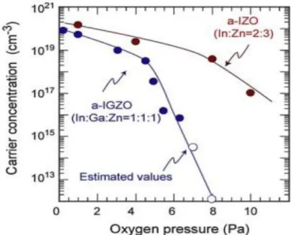
tail-states, as shown in Fig. 1-3. [12]
Fig. 1-3 Schematic orbital drawing of electron pathway (conduction band bottom) in conventional silicon-base semiconductor and ionic oxide semiconductor. [12]
In contrast, transport oxides constituting of heavy post transition metal cat-ions with the
(n-1)d10ns0 electron configuration, where n≧5, are the transparent AOS (TAOS) candidates
having large mobility comparable to those of the corresponding crystals. [13] The electron
pathway in oxide semiconductor is primarily composed of spatially spread ns orbital with an
orbital is possible. The degree of overlap of the ns orbital is insensitive to the distorted
metal-oxygen-metal bonding. This feature shows why the Hall mobility of AOSs is similar to
the corresponding crystalline phase, even under the room temperature deposition of
1.2.3 Amorphous In-Ga-Zn-O TFTs
Among the TAOS materials, amorphous indium gallium zinc oxide (a-IGZO) is one of
the most glaring candidates serving as semiconductor layer in thin film transistor (TFT). [14]
However there are still many critical issues existed in a-IGZO TFT, especially for the easy
absorption and desorption reaction of the oxygen atom with the surrounding atmosphere. As
the oxygen species are absorbed from the ambient atmosphere, they can capture electrons in
the conducting channel and form a depletion region beneath back channel layer. By following
the equation of O g e O s 2 ) (
2 , the resultant buildup of absorbed negative space
charges O2-(s) easily repells conduction electrons and positively shifts Vth of a-IGZO TFT. [14]
Whereas the desorption of oxygen atoms in a-IGZO back channel will result in the left shifts
of Vth. This random reaction of absorption and desorption happening also leads to some
uniformity problems. Some researching groups have applied passivation layer method to
shield the back channel from the contact with ambient air. But the sequel processes would
strongly affects the original properties of a-IGZO film. Therefore, the fundamental method to
release the issue of environmental influence should be the improvement of the film quality of
itself.
TAOSs have attracted keen attention since the high performance thin-film transistors can
by obtained by using the amorphous In-Ga-Zn-O (a-IGZO) thin films for the semiconductor
TFT performance is also confirmed by using the sputter deposition [15], which demonstrates
the possibility of the large-area applications. The dependence of the TFT characteristics on the
metal composition is investigated in detail by a novel combinational approach, since the
multi-metal AOSs can take any ratios of the composition.
The a-IGZO film has electrons as majority carriers, which is mainly affected by the
oxygen vacancies and oxygen interstitials during deposition processes. [16] The ion bonding
structure makes the a-IGZO TFT exhibit high field-effect carrier mobility even in the
amorphous phase. [17] Even if the a-IGZO TFT owns many superior characteristics, the
sensitivity to atmosphere is a extremely critical issue for the a-IGZO TFT application. [18]
The environment-dependent metastability was attributed to oxygen adsorption/desorption
reactions to the backchannel of the a-IGZO TFT device. The random reactions between the
ambient air and the a-IGZO backchannel layer can not only change the oxygen vacancies in
the a-IGZO film but result in a threshold voltage shift with days going by, and even device
uniformity problems. [19] In addition to isolate the a-IGZO layer from exposing to the
atmosphere, the electrical stability and uniformity of the a-IGZO film can be improved by the
optimization of the chemical stoichiometry or adjusting oxygen content inherently.
For the In2O3-Ga2O3-ZnO ternary system, the incorporation of cat-ions with large ionic
valance such as Ga3+ and Al3+ to high conductive oxides such as In2O3 and ZnO is effective to
such as a-ITO and c-ZnO have high density carrier density, hence is difficult to control the
device characteristics. Besides, amorphous In-Ga-Zn-O (a-IGZO) is transparent throughout
the visible spectrum. The transmittance is greater than 80 percent from 400 nm to 850 nm as
shown in Fig. 1-4. [21] Because only In3+ meets the electron configuration criterion
(n-1)d10ns0 (n≧5) of heavy post transition metal cat-ion for ionic AOS (IAOS) among the
three cations. The mobility is primary determined by the fraction of In2O3 content and the
highest value of ~40 cm2(Vs)-1 is obtained for the samples containing the maximum In2O3
fraction. The large ionic valence ions such as Ga3+ combine with high conductive oxides such
as In2O3 and ZnO to control the carrier concentration effectively because of the strong
metal-oxygen bonds. [22] In other words, Ga3+ suppresses carrier generation via oxygen
vacancy formation because Ga ion forms stronger bond with oxygen than Zn and In ion. [23]
Therefore, the InGaZnO4 composition was chosen as the AOS for channel layer of the
transparent TFT. A critical issue of semiconductor materials for TFT applications is
Wavelength (nm) 300 400 500 600 700 % T 50 60 70 80 90 100
Fig. 1-4 Transmittance of a-IGZO film in visible light region. [21]
This is particularly important for AOSs because electron carriers can be easily generated.
It is vital to choose materials which control carrier concentration at low levels (~1014 cm-3) to
achieve low off current (I off) and large on-off current ratio (Ion/I off). [24] In practice, the
effect of binary amorphous materials in the In2O3-ZnO system is employed in commercial
flexible transparent conductive films by depositing on plastic sheet. Thus, the effect of partial
oxygen pressure was studied on the carrier concentration in a-InGaZnO4 and a-In2Zn3O6 and
the results are shown in Fig. 1-5. [25] The carrier concentration in the a-InGaZnO4 is
distinctively reduced to below 1013 cm-3 by increasing PO2 to 8 Pa, on the other hand, it
remains at 1018 cm-3 in the a-In2Zn3O6 deposited under the same condition. It is evident that
incorporation of Ga3+ is supposed to attract the oxygen ions tightly due to its high ionic
around the chemical composition of InGaZnO4 is not sensitive to the variation in the
composition, as shown in Fig. 1-5. [26] Thus, the InGaZnO4 system has better electrical
properties than the In2Zn3O6 system. [27] In addition, the a-IGZO TFTs’ processes are similar
to that of a-Si based TFT. It means the existing production lines can be used. In this case, we
can save a lot of money from buying new equipment.
Fig. 1-5 The carrier concentration as a function of O2 pressure during the deposition in a-
1.3 Microwave Annealing
1.3.1 Interaction of Microwaves with Matter
Conventional heating usually involves the use of a furnace, which heats the walls of the
furnaces by convection or conduction. The core of the sample takes much longer to achieve
the target temperature. Microwave heating is able to heat the target compounds without
heating the entire furnace, which saves time and energy. It is also able to heat sufficiently thin
objects throughout using volumetric heating, rather than through the outer surface. Different
materials convert microwave radiation to differing amounts of heat. The selectivity of
different materials allows the object to be heated at differing speeds as well. [34] [38]
Microwave heating is the perspective techniques, which heat the volume of the wafer,
not just its surface. It used very loosely for electromagnetic radiation in millimeter and radio
frequency spectrum. Microwave processing is quite the same in thermal processing of ceramic
materials. In 1990, Buchta used a microwave generator operating at 2.45GHz and a power
about 1500W to heat 5-inch wafers 125mm to about 1000oC over period of a few seconds.
Recently Thompson and his group used a resonant chamber with a magnetron source. Dr.
Bykov used a 30 GHz gyration device and a resonant processing chamber. They only
demonstrated that microwave can activate at high temperature. In 2007, Jeff M. Kowalski
report that microwave can activate of the heavily doped implanted layers in the range of
situation, and can keep doped less diffusion. The conventional heating is only limited by thermal diffusivity and surface temperature. So, the deep of surface can’t receive the heating energy. But microwave generate heat directly inside the exposed material as result of
molecular motion. Energy is transferred throughout the entire wafer. [29] Therefore, the
effective of activated is more than conventional heating. Electromagnetic (EM) radiation is a
very crucial form of energy available to mankind. It consists of electric and magnetic fields
that fluctuate sinusoidally in planes perpendicular to each other and propagate at the speed of
light. EM radiation does not need a medium to in which to travel. [30] The dual nature of EM
radiation is evident through its wave-like behavior in the case of interference and diffraction
and its particle-like behavior in the case of phenomena like the photoelectric effect. The
quanta of EM radiation are termed as photons. The frequency ν and the wavelength λ are inversely proportional to each other, related by ν = c/λ, where c is the speed of light in vacuum. The energy E of the EM radiation depends linearly on the frequency ν, given by E = h ν where h is the Planck’s constant. [31]
The electromagnetic spectrum is classified into regions of increasing frequencies (or
equivalently, energies): radio waves, microwaves, infrared, visible light, ultraviolet, X-rays,
and gamma rays. Microwaves are generally taken to have frequencies from 300 MHz to 300
GHz which correspond to wavelengths of 1 m down to 1 mm, respectively. Microwaves have
RADAR, electronic warfare, radiation therapy, non-destructive testing of materials, etc. [32]
The interaction of microwaves with materials takes place through the two components of
the microwave radiation: the electric field E and the magnetic field H. The response of a
material when exposed to an electromagnetic radiation may be understood through the
dielectric constant ε of the material. The dielectric constant, also known as the permittivity of
the material, describes the ability of the material to be polarized in the applied electric field.
To understand the dielectric response to sinusoidal fields such as the microwaves, complex
permittivity ε* is employed: ε* = ε’ + i ε”. The real part of the dielectric constant is a measure
of the penetration of microwave energy in the material; while, the imaginary part indicates the
ability of the material to store the energy. The dielectric properties vary with temperature and
frequency. [33]
In any given material, various entities such as the free electrons, valence electrons, ions,
molecular dipoles, and interfacial charges respond to the applied electric and magnetic field.
The sinusoidal fields cause the charged species to polarize and vibrate. Different charged
species all have different natural frequencies of vibration. The conversion to heat occurs
because of the lag of the response of the material to the applied electromagnetic field. In the
heating of dielectric materials, it is assumed that the magnetic field does not contribute to
microwave absorption and the heating occurs entirely due to the electric field.
a. Electronic polarization: When an atom is subjected to an external electric field,
displacement of the electron cloud with respect to the nucleus gives rise to formation of
a dipole. Valence electrons shift much more easily than the tightly bound core electrons.
Covalent crystals have large dielectric constants owing to the displacement of the valence electrons. Thus, materials like silicon (εr’=11.9) and germanium (εr’=11.9) have high real components of the dielectric constant; hence, microwaves easily
penetrate these materials.
b. Dipole polarization: Under the application of an external electric field, polar molecules
orient themselves with the field. The lag associated with this response and the
inter-molecular collisions lead to dielectric heating. In some materials, the polarization
can be retained due to the need for thermal activation for molecular rotation, which gives rise to the formation of “electrets”.
c. Ionic or atomic polarization: Relative displacement of the positive and negative ions or
atoms within molecules and crystal structures from their equilibrium lattice sites gives
rise to ionic polarization.
d. Interfacial polarization: This involves the accumulation of free charges at interfaces
located within the material: grain boundaries, phase boundaries and defect regions.
Under the application of an electric field, the mobile charges are displaced and
1.3.2 Microwave Processing of Materials
Microwaves generate rapidly changing electric fields and will generally heat any
material containing mobile electric charges, such as polar molecules in a solvent or
conducting ions in a solid. Polar solvents are heated as their component molecules are forced
to rotate with the field and lose energy in collisions. Microwave heating a material depends to a great extent on its ‘dissipation’ factor, which is the ratio of dielectric loss or ‘loss’ factor to dielectric constant of the material. The dielectric constant is a measure of the ability of the
material to retard microwave energy as it passes through; the loss factor is a measure of the ability of the material to dissipate the energy. In other words, ‘loss’ factor represents the amount of input microwave energy that is lost in the material by being dissipated as heat. [35]
Therefore, a material with high loss factor is easily heated by microwave energy. In fact, ionic
conduction and dipolar rotation are the two important mechanisms of microwave energy loss
(i.e. energy dissipation in the material).
Microwaves are reflected from the surface and therefore do not heat metals. Metals in
general have high conductivity and are classed as conductors. Conductors are often used as
conduits (waveguide) for microwaves. Materials which are transparent to microwaves are
classed as insulators. Insulators are often used in microwave ovens to support the material to
be heated. Materials which are excellent absorbers of microwave energy are easily heated and
Non-homogeneous material (in terms of dielectric property) may not heat uniformly, that
is, some parts of the materials heat faster than others. This phenomenon is often referred to as
thermal runaway. This condition can be minimized by keeping the sample in mixing or
fluidized condition. Volumetric heating is the key characteristic of microwave processing. In
conventional heating, the thermal energy is transferred to the material from the outside to the
inside, creating a temperature gradient. Small penetration depth of infrared (less than 0.1 mm)
leads to energy deposition being limited to the surface layers. [37] Microwave heating
overcomes this through absorption of the microwave energy throughout the volume of the
material. Since the surface loses energy by radiation, the core of the material is usually hotter
and the temperature profile is the inverse of that seen in conventional heating. Volumetric
heating has the advantage of uniform and rapid processing of materials leading to an
increased throughput. Rapid heating in semiconductors provides the advantage of minimal
diffusion of various species into the substrate.
Poorly absorbing materials (those with small values of ε”) can be hard to heat using microwaves. One common solution to this is the use of microwave susceptors to provide
hybrid heating. [38] Microwave processing can also be employed for selective heating of
1.4 Thesis Organization
This thesis is divided into four chapters. The main purpose of my thesis is to develop an new process method to improve the TFTs’ characteristics. In my thesis, I use a-IGZO as my active layer for increasing the performance of device. Then developed new processing method: MWA for enhancing TAOS and transistor’s characteristics. We will discuss the intrinsic electrical characteristics, stability and reliability in the following pages.
In chapter 1, the brief overview of flat display panel industry, operations of the TFT-LCD, the carrier transport mechanism of AOSs, amorphous In-Ga-Zn-O TFTs and microwave annealing method are introduced.
In chapter 2, the experiment procedures are introduced. The sputtering system and microwave heating system are also described. The measurement and extraction of electrical parameters are also described. The measurement of reliability on a-IGZO TFTs is described.
In chapter 3, the intrinsic electrical characteristics of a-IGZO TFTs with different MWA
time and power with two kind of gate insulator (SiO2 and SiNx) were discussed. Then we will
discuss the comparison of MWA annealing and furnace annealing. Then we will show the results of material analysis with UV-visible, X-ray diffraction, scanning electron microscope and X-ray photoelectron spectroscopy.
Chapter 2 Experiment Procedures
2.1 Experiment Procedures
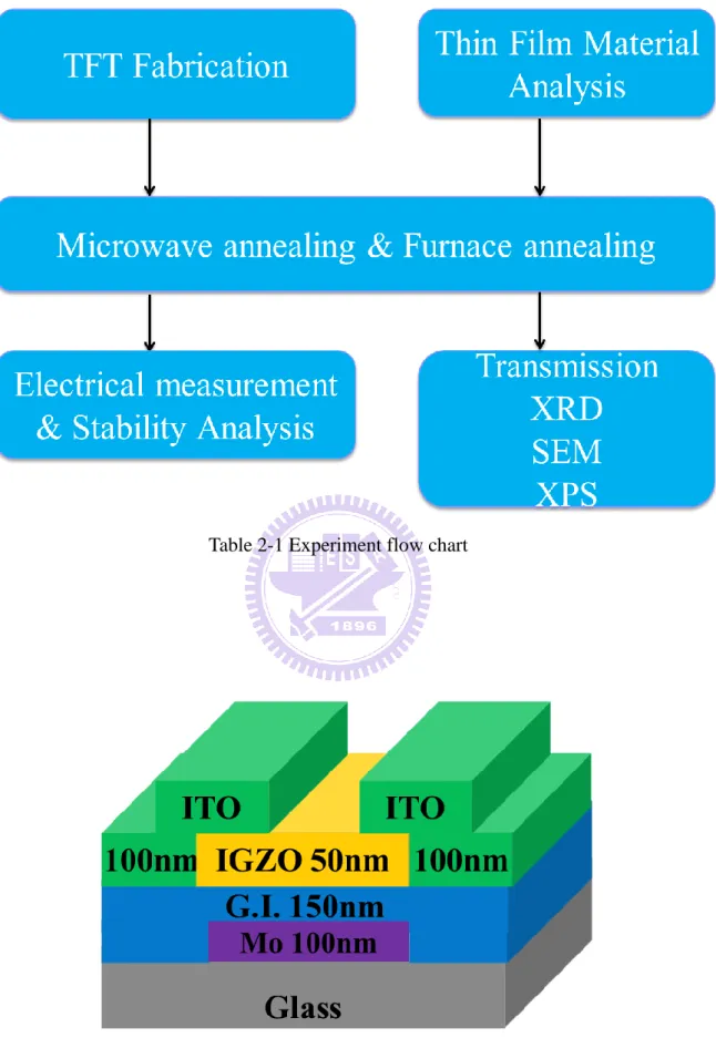
Table 2.1 is the experiment flow path in my experiment. First of all, we fabricate the TFT
device we want. Then we do different treatment to our device. The special part is we will do
microwave annealing to our device after they are fabricated. The treatment can be classified to
two ways, one is electrical analysis and the other is material analysis.
The TFT devices were chosen as a bottom-gated passivation-free inverted staggered
structure and fabricated on a glass substrate. First, a 100-nm-thick Mo layer was formed as a
gate electrode in a dc sputtering system and a 150-nm-thick silicon nitride (SiNx) was
subsequently deposited on the patterned gate electrode by plasma-enhanced chemical vapor
deposition (PECVD). The active channel layer of a 50-nm thick IGZO layer was formed by
dc sputtering with a power of 100 W at room temperature in argon (Ar) ambiance with flow
rate 10 SCCM (SCCM denotes cubic centimeter per minute at STP) with target of In:Ga:Zn:O
= 1:1:1:4 at.%. The sputtering was carried out at a working pressure of 3 x 10⁻³ torr and the
base pressure was below 5 x 10⁻⁶ torr. Then, a 100-nm-thick indium tin oxide (ITO) was
formed serving as source/drain electrodes by RF sputtering system and all the layers were
defined by shadow mask. The channel width and length of a-IGZO TFTs were varied from 200 to 1000 μm. As we see at Fig. 2-1. Sequentially, all samples were microwave annealed at
was denoted as microwave power 600~700 W for annealing time 100s. The MWA processing
time is defined as the period when the microwave power was turned on. In our experiment,
the 5.8GHz microwave source has been employed for annealing process. A sample with
conventional thermal annealing process was also fabricated at 450 °C for 1 h in a furnace with
N2 gas flow rate of 10L/hr under atmosphere pressure for comparison. All electrical and
reliability measurements were carried out by using the semiconductor parameter analyzer,
Keithley 4200. For the X-ray photoelectron spectroscopy measurement, X-ray diffraction,
scanning electron microscope, 50-nm a-IGZO thin films with different microwave annealing
conditions were deposited separately on n-type Si wafer. And measure transmittance with
Table 2-1 Experiment flow chart
2.2 Sputtering systems
The experimental methods of the fabrication of the a-IGZO TFT are described. Besides,
the principle of sputtering system including the RF sputtering and the DC sputtering is
described. In this chapter, we will introduce two sputtering systems. One is RF sputtering and
the other is DC sputtering.
RF sputtering can be applied to the deposition of both insulating conducting materials.
The substrate is located above the target so that the sputtered atoms can be deposited on to the
substrate. A RF power supply generates plasma at the frequency of 13.56 MHz. A RF
sputtering system is shown in Fig. 2-2. [39]
DC sputtering has the advantage of higher deposition rate and is less expensive than RF
sputtering. A DC sputtering is shown in Fig. 2-3 [40], the substrate is located above the target
and acts as the anode. DC sputtering is commonly applied to deposit conductive materials.
The plasma creates ions which are accelerated towards the target by a negative DC bias on the
target. The ions bombard the target surface and dislodge the target atoms, which then deposit
onto the substrate. The sputtering is performed in vacuum, typically between 1 mTorr and 50
mTorr. A lower chamber pressure increases the mean free path, which is the distance between
Fig. 2-2 Schematic RF sputtering system [39]
2.3 Basic Microwave Heating System
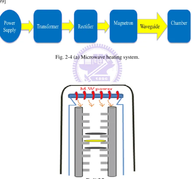
The microwave heating system is made up of four basic components: power supply,
magnetron, applicator for the heating if the target material and waveguide for transporting
microwaves from the generator to the applicator. Fig. 2-4(a) shows a simplistic diagram of the
microwave heating system.
The microwave system mainly contains: [38]
a. Microwave power supply: supplies high voltage power for the microwave source. Supply
includes internal alarms to prevent damage the microwave source, i.e. over volt alarm or
over temperature alarm.
b. Microwave source: generates the microwave energy required for processing. Internal
interlocks prevent overheating, i.e. water flow switch or over temperature sensor.
c. Isolator: eliminates excessive microwave energy form the process chamber to prevent
damage to the microwave source.
d. Coupler: a port to measure forward microwave energy going into the process chamber.
e. Waveguide: delivers generated microwave energy into the process chamber.
f. Process chamber: an octagonal prism and vessel designed to isolate wafers from the
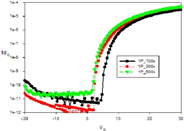
atmosphere while gases and microwave as specified by the recipe are applied to the wafers. The chamber’s geometry promoted a uniform microwave energy field. As the Fig. 2-4 (b). [38]
When the process starts, the loading stage under the process chamber sealed. And then,
the stage rotates slowly for increase the uniformity of the microwave absorption. After ten
minutes N2 gas pre-purge, the microwave power supplies turns on. The susceptors above and
below the wafer can prevent particles from the environment during process. The addition of
filler wafers (bare silicon) above and below the process wafer can prevent plasma generation.
[39]
Fig. 2-4 (a) Microwave heating system.
Fig. 2-4(b) The setup in the microwave chamber. The distance between adjacent slots was 1 cm only. [38]
2.4 Parameter Extraction Method
The device electrical properties were measured by a Keithley 4200 IV analyzer in a
light-isolated probe station at room temperature. In IDS-VGS measurement, the typical
drain-to-source bias was swept from VGS=-20 V to VGS=30 V. In this session, we describe the
methods of typical parameters extraction such as threshold voltage (Vth), subthreshold swing
(SS) and field effect mobility (
μ
FE) from device characteristics.Threshold voltage (Vth) was defined from the gate to source voltage at which carrier
conduction happens in TFT channel. Vth is related to the gate insulator thickness and the flat
band voltage. Plenty of methods are available to determine Vth which is one of the most
important parameters of semiconductor devices. This thesis adopts the constant drain
current method, which is, the voltage at a specific drain current NID is taken as Vth, that is, Vth
= VG (NID) where Vth is threshold voltage and NID stands for normalized drain current.
Constant current method is adopted in most studies of TFTs. It provides a Vth close to that
obtained by the complex linear extrapolation method. Generally, the threshold current NID =
ID/(W/L) is specified at 1 nA in linear region and at 10 nA in saturation region; W and L
represent for TFT channel length and width, respectively. [41]
Subthreshold swing (SS, V / dec.) is a typical parameter to describe the control ability of
gate toward channel which is the speed of turning the device on and off. It is defined as the
magnitude. SS is related to the process, and is irrelevant to device dimensions. SS can be
lessened by substrate bias since it is affected by the total trap density including interfacial trap
density and bulk density. In this study, SS was defined as one-half of the gate voltage required
to decrease the threshold current by two orders of magnitude (from 10-8A to 10-10A). [41] The
threshold current was specified to be the drain current when the gate voltage is equal to Vth.
Typically,
μ
FE is determined from the transconductance (gm) at low drain bias (VD = 0.1V). [41] The TFT transfer I-V characteristics can be expressed as
] 2 1 ) [( C μ = ID FE ox VG Vth VD VD2 L W (2-1) Where,
COX is the gate oxide capacitance per unit area,
W is channel width,
L is channel length,
Vth is the threshold voltage.
If VD is much smaller than VG – Vth (i.e. VD << VG – Vth) and VG > Vth, the drain current
can be approximated as:
D th G V V V L W ) ( C μ = ID FE ox (2-2)
The gm is defined as:
D V L W ox FE m =μ C g (2-3) Thus, m g WV C L μFE (2-4)
2.5 Measurement of reliability on a-IGZO TFTs
In this session, we will introduce two ways of reliability’s measurement. One is gate DC bias stress condition and the other is light illumination’s measurement.
The DC gate bias stress condition was set to VG = +37.5 V for Positive Gate Bias stress
(PGBS) and VG = -37.5 V for Negative Gate Bias Stress (NGBS). Converted into electric field
(E) is 2.5 MV/cm, while source and drain electrodes are connected to ground from 0s to
2000s. The sample was stressed at room temperature (25℃).
The devices was place in the dark environment (in the black box) and under room
pressure and temperature. Table 2-2 shows the experiment flow of devices under light
illumination. The a-IGZO TFTs with different annealing conditions were measured under
different wavelength light which ranged from 900 nm (visible light) to 300 nm (UV light).
The light source was a halogen optic lamp from OSRAM Inc. at 150 W generating light
intensity about 63315 lx. We find the devices fabricated by the standard manufacturing
processes should be placed in the box for few minutes even few hours to get stable electrical
performances. And light_1_on means the specific wavelength illumination on device under
measuring.
Chapter 3 Results and Discussion
3.1 The effect of different MWA time on a-IGZO TFT
3.1.1 a-IGZO TFT with SiO
2gate insulator
First, we discuss the intrinsic characteristics of SiO2 gate insulator. The drain-to-source
voltage (VDS) was fixed at 10 V. The gate-to-source voltage (VGS) was varied from -20 V to
30 V. We fix the MWA power to 1P (600~700W) and change the MWA annealing time for
100s / 300s / 600s. Fig. 3-1 shows the results of SiO2 gate insulator with different MWA time.
We can see the line of 100s is obviously different from the other two. Table 3-1 gives us more
specific results about different MWA time affect to the a-IGZO TFT with SiO2 gate insulator.
We can find that for annealing time 100s to 300s have great increases in mobility and decrease
the amounts of SS / Vth. For the condition of MWA time 600s, we can find that it has almost
the same mobility, Vth and SS value as the condition of MWA time 300s.
Table 3-1 The data of MWA different time for SiO2 gate insulator
Second, we will discuss the reliability of different MWA time with SiO2 gate insulator.
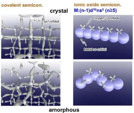
Fig.3-2 shows Vth variation of a-IGZO TFTs after being gate bias stressed with electrical field
of 2.5 MV/cm for 2000s in atmosphere. Vth shifted in the direction of positive voltages under
positive gate bias stress (PGBS). The shift amounts decrease with higher MWA time. On the
other hand, we can find that negative gate bias stress (NGBS) didn’t shift a lot. We find the
shift amounts of Vth don’t have obvious difference through NGBS.
Second(s) 0 500 1000 1500 2000 -1 0 1 2 3 4 5 6 7 8 9 10 11 12 13 1P_100s 1P_300s 1P_600s
3.1.2 a-IGZO TFT with SiN
xgate insulator
First, we discuss the intrinsic characteristics of SiNx gate insulator. The VDS was fixed at
10 V. The gate-to-source voltage (VGS) was varied from -20 V to 30 V. We fixed the MWA
power to 1P (600~700W) and changed the MWA annealing time for 100s / 300s / 600s. Fig.
3-3 shows the results of SiNx gate insulator with different MWA time. We can see the line of
1P_100s is obviously different from the other two. Table 3-2 gives us more specific results for
different MWA time the a-IGZO TFT with SiNx gate insulator. We can find that for annealing
time 100s to 600s have great increases in mobility and decrease the SS / Vth. For the condition
of MWA time 600s, we can find it has the best results than the other two.
Second, we will discuss the reliability of different MWA time with SiNx gate insulator.
Fig.3-4 shows Vth variation of a-IGZO TFTs after being gate bias stressed with electrical field
of 2.5 MV/cm for 2000s in atmosphere. Vth shifted in the direction of positive voltages under
positive gate bias stress (PGBS). The shift amounts decrease with higher MWA time. On the
other hand, we can find that negative gate bias stress (NGBS) didn’t shift a lot. We find the
shift amounts of Vth don’t have obvious difference through NGBS.
Second(s) 0 500 1000 1500 2000 -1 0 1 2 3 4 5 6 7 8 9 10 11 12 13 14 15 16 17 1P_100s 1P_300s 1P_600s
3.2 The effect of different MWA Power on a-IGZO TFT
3.2.1 a-IGZO TFT with SiO
2gate insulator
First, we discuss the intrinsic characteristics of SiO2 gate insulator. VDS was fixed at 10 V.
VGS was varied from -20 V to 30 V. We fixed the MWA time to 100s and changed the MWA
annealing time for 1P (600~700W) and 2P (1200~1400W). Fig. 3-5 shows the results of SiO2
gate insulator with different MWA time. Table 3-3 gives us more specific results for different
MWA power the a-IGZO TFT with SiO2 gate insulator. We can find that for annealing power
1P (600~700W) to 2P (1200~1400W) have great increases in mobility and decrease the SS /
Vth.
Second, we will discuss the reliability of different MWA time with SiO2 gate insulator.
Fig.3-6 shows Vth variation of a-IGZO TFTs after being gate bias stressed with electrical field
of 2.5 MV/cm for 2000s in atmosphere. Vth shifted in the direction of positive voltages under
positive gate bias stress (PGBS). The shift amounts decrease with higher MWA power. On the other hand, we can find that negative gate bias stress (NGBS) didn’t shift a lot. We find the
shift amounts of Vth don’t have obvious difference through NGBS.
Second(s) 0 500 1000 1500 2000 -1 0 1 2 3 4 5 6 7 8 9 10 11 12 13 1P_100s 2P_100s
3.2.2 a-IGZO TFT with SiN
xgate insulator
First, we discuss the intrinsic characteristics of SiNx gate insulator. VDS was fixed at 10 V.
VGS was varied from -20 V to 30 V. We fixed the MWA time to 100s and changed the MWA
annealing time for 1P (600~700W) and 2P (1200~1400W). Fig. 3-7 shows the results of SiNx
gate insulator with different MWA time. Table 3-3 gives us more specific results about
different MWA power the a-IGZO TFT with SiNx gate insulator. We can find that for
annealing power 1P (600~700W) and 2P (1200~1400W) has great increases in mobility and
decrease the SS / Vth.
Second, we will discuss the reliability of different MWA time with SiNx gate insulator.
Fig.3-8 shows Vth variation of a-IGZO TFTs after being gate bias stressed with electrical field
of 2.5 MV/cm for 2000s in atmosphere. Vth shifted in the direction of positive voltages under
positive gate bias stress (PGBS). The shift amounts decrease with higher MWA time. On the
other hand, we can find that negative gate bias stress (NGBS) didn’t shift a lot. We find the
shift amounts of Vth don’t have obvious difference through NGBS.
Second(s) 0 500 1000 1500 2000 -1 0 1 2 3 4 5 6 7 8 9 10 11 12 13 14 15 16 17 1P_100s 2P_100s
3.3 The Comparison of MWA and Furnace Annealing on a-IGZO
TFT
3.3.1 a-IGZO TFT with SiO
2gate insulator
First, we discuss the intrinsic characteristics of SiO2 gate insulator. VDS was fixed at 10 V.
VGS was varied from -20 V to 30 V. We chose the best two conditions: 1P_300s and 1P_600s,
comparing with furnace annealing. Fig. 3-9 shows the results of SiO2 gate insulator with
different MWA conditions and furnace annealing. Table 3-5 gives us more specific results of
different MWA conditions and furnace annealing affect to the a-IGZO TFT with SiO2 gate
insulator. We can find that for the condition of MWA time 300s and 600s have the similar
results, comparing with furnace annealing, we can find that MWA has great increases in
mobility and decrease the SS / Vth.
Fig. 3-9 Electrical characteristic comparison with MWA and furnace annealing for SiO2 gate
Table 3-5 The data of comparison with MWA and furnace annealing for SiO2 gate insulator
Second, we will discuss the reliability of different MWA time with SiO2 gate insulator.
Fig.3-10 shows Vth variation of a-IGZO TFTs after being gate bias stressed with electrical
field of 2.5 MV/cm for 2000s in atmosphere. Vth shifted in the direction of positive voltages
under positive gate bias stress (PGBS). The shift amounts decrease with higher MWA time
and almost the same as furnace annealing for the condition of MWA time 600s. On the other hand, we can find that negative gate bias stress (NGBS) didn’t shift a lot. We find the shift
amounts of Vth don’t have obvious difference through NGBS.
Second(s) 0 500 1000 1500 2000 -1 0 1 2 3 4 5 6 7 8 9 10 11 12 13 1P_300s 1P_600s furnace
3.3.2 a-IGZO TFT with SiN
xgate insulator
First, we discuss the intrinsic characteristics of SiNx gate insulator. VDS was fixed at 10 V.
VGS was varied from -20 V to 30 V. We chose the best two conditions: 1P_ 600s and 2P_100s,
comparing with furnace annealing. Fig. 3-11 shows the results of SiNx gate insulator with
different MWA conditions and furnace annealing. Table 3-6 gives us more specific results
about different MWA conditions and furnace annealing affect to the a-IGZO TFT with SiNx
gate insulator. We can find that for annealing time comparing with furnace annealing, MWA
condition for 1P_600s have great increases in mobility and decrease the SS / Vth.
Fig. 3-11 Electrical characteristic comparison with MWA and furnace annealing for SiNx gate
Table 3-6 The data of comparison with MWA and furnace annealing for SiNx gate insulator
Second, we will discuss the reliability of different MWA time with SiNx gate insulator.
Fig.3-12 shows Vth variation of a-IGZO TFTs after being gate bias stressed with electrical
field of 2.5 MV/cm for 2000s in atmosphere. Vth shifted in the direction of positive voltages
under positive gate bias stress (PGBS). The shift amounts decrease for MWA condition of
2P_100s and almost the same as furnace annealing. On the other hand, we can find that
negative gate bias stress (NGBS) didn’t shift a lot. We find the shift amounts of Vth don’t have
obvious difference through NGBS.
Second(s) 0 500 1000 1500 2000 -1 0 1 2 3 4 5 6 1P_600s 2P_100s furnace
Fig. 3-12 The PBIS and NBIS comparison of MWA and furnace annealing for SiNx gate
3.4 Material Analysis Results
In this chapter, we will introduce four different material analysis results. First is
UV-visible, second is X-ray diffraction, third is scanning electron microscope and the last is
X-ray photoelectron spectroscopy.
First, a-IGZO TFTs with different annealing treatment were measured under different
wavelength light which ranged from 900 nm (visible light) to 300 nm (UV light). The
decrease of the light transmittance in UV light region can be attributed to the decrease of
optical energy band-gap (Eg). The optical band-gap extract from different wavelength’s
transmittance of each condition was collected and compared in Table 3-7. It was clearly observed that the film didn’t change their band-gap a lot from different MWA time and power. Comparing with furnace annealing, it’s still not change their band-gap a lot. Which means that after post-annealing the transmittance didn’t have obvious difference.
Table 3-7 The data of optical band-gap for different MWA time / power and furnace annealing
Second, X-ray diffraction (XRD) is used to observe the active layer pattern shapes and
continue time is 1 second. Fig. 3-13 shows the results of a-IGZO TFTs with difference
annealing conditions for 50nm by XRD. We can find that the XRD results for different MWA time and power didn’t change films structure. Comparing with furnace annealing, MWA still remain amorphous phase. So we can find that different annealing treatment didn’t change the films structure.
Fig. 3-13 The X-ray diffraction results for different MWA time / power and furnace annealing
Third, scanning electron microscope (SEM) images indicate the formations of films
surface structure. Fig 3-14 shows the results of SEM for different annealing conditions. We can find that different MWA time and power didn’t change the surface of films. Comparing with furnace, it’s still have obvious difference between MWA. So we can find that different
.
Fig. 3-14 The scanning electron microscope results for different MWA time / power and furnace annealing
The last, I will show the X-ray photoelectron spectroscopy (XPS) results. The results of XPS analysis on O1s spectrum in each a-IGZO thin film was showed in Fig. 3-15. Fig. 3-15 shows the XPS analysis results of O1s spectrum for the a-IGZO thin film with microwave annealing treatments. Two components of O1s peaks could be fitted by Gaussian Lorentzian deconvolution, which centered at 530.6 and 531.4 eV, respectively. The lower binding energy centered at 530.6 eV, denoted as peak A, originated from the lattice oxygen ions with neighboring metal atoms. [42] The higher binding energy peak at 531.4 eV, denoted as peak B, corresponds to O2_ ion at an oxygen-deficient region in the matrix of the a-IGZO film. [43] According to the results of XPS, peak A increased and peak B decreased while the microwave annealing duration increased, as shown in Fig. 3-15. Also, the XPS spectrum of a-IGZO film with high-power microwave annealing was composed of a high intensity of peak A and low intensity of peak B. This figure revealed a high content of lattice oxygen ions in the microwave-annealed a-IGZO films with few oxygen-deficient regions as the microwave
assisted the oxygen ions binding with metal atoms and suppressed the formation of oxygen-deficient region in the a-IGZO films when increasing both the microwave power and annealing duration.
Fig. 3-15(b) shows the XPS O1s spectrum of a-IGZO thin film with 2P microwave
annealing for 100 s and furnace annealing at 450oC for 1 hour for comparison. The O1s peak
of a-IGZO film with microwave annealing composed of a higher intensity of peak A and a
lower intensity of peak B than those of the 450oC furnace-annealed one. These material
analysis results were consistent with the electrical improvement in device performance and reliability of a-IGZO TFT, since microwave annealing facilitated the formation of lattice oxygen and eliminated the defects originating from oxygen deficiency. Energy transfer to the a-IGZO TFT was even more effective by the microwave annealing process than that of the conventional furnace annealing.
Chapter 4 Conclusions
4.1 Conclusions
According to the statements of previous chapter, we can have the following conclusions. After 1P_300s MWA treatment, it was observed that the a-IGZO TFTs represented a lower threshold voltage (it changes from 3.53V to 3.13V), a lower sub-threshold swing (it changes
from 1.25 V/dec. to 0.62 V/dec.), and a higher mobility (it changes from 5.33 cm2/V-s to 5.81
cm2/V-s) for SiO2 gate insulator. After 1P_600s MWA treatment, it was observed that the
a-IGZO TFTs represented a lower threshold voltage (it changes from 1.12V to 1.02V), a lower sub-threshold swing (it changes from 0.41 V/dec. to 0.30 V/dec.) and a higher mobility
(it changes from 11.7 cm2/V-s to 13.4 cm2/V-s) for SiNx gate insulator. The stability also get
great improve by MWA. We can find that the shift amounts of Vth were decrease with
increasing MWA time and power for both two different G.I. under the PBIS.
Through material analysis of UV-visible, XRD and SEM, we can find that the optical band-gap, phase structure, grain size and the ratio of atom composition of a-IGZO thin films were not damaged by different kind of post-treatments. But when see the results of XPS, we can find that the oxygen defects were repaired and the oxygen bonding was become stronger by increasing MWA time and power.
We can find that MWA can have the performance as good as (even better than) furnace annealing for low thermal budget and short working time. This method has great potential for applying in high-resolution display products and flexible electronics.
In summary, this work has demonstrated the feasibility of high performance and reliable a-IGZO TFTs with microwave annealing process. Microwave annealing with low thermal budget can reduce the manufacturing process period and improve electrical characteristics of
a-IGZO TFTs, due to the effective absorption of microwave energy by the a-IGZO active layer. This selective heating also potentially avoided the damage to materials neighboring the a-IGZO channel layer in the TFT device structure during thermal processes. With optimum microwave annealing around 1200W for 100s in this work, electrical performance and reliability of a-IGZO TFT are more significantly promoted than with furnace annealing at
450oC for 1h. Results of this study significantly contribute to microwave annealing
![Table 1-1 The comparison of a-Si TFT, poly-Si TFT and TAOSs TFT [5]](https://thumb-ap.123doks.com/thumbv2/9libinfo/8448775.182352/14.892.168.828.699.1071/table-comparison-si-tft-poly-tft-taoss-tft.webp)
![Fig. 1-4 Transmittance of a-IGZO film in visible light region. [21]](https://thumb-ap.123doks.com/thumbv2/9libinfo/8448775.182352/22.892.259.674.137.452/fig-transmittance-igzo-film-visible-light-region.webp)
![Fig. 2-3 Schematic DC sputtering system [40]](https://thumb-ap.123doks.com/thumbv2/9libinfo/8448775.182352/35.892.268.699.550.908/fig-schematic-dc-sputtering-system.webp)