國
立
交
通
大
學
機械工程學系
博
士
論
文
利用射頻反應磁控濺鍍方式來研究
氧 化 鋅 薄 膜 之 材 料 特 性 與 電 漿 特 性 之 關 係
Investigation of Relationship between the Plasma and
Material Characteristics of Zinc Oxide (ZnO) Thin Film
by Radio Frequency (RF) Reactive Magnetron Sputtering
研 究 生:許哲維
指導教授:吳宗信 博士
利用射頻反應磁控濺鍍方式來研究
氧化鋅薄膜之材料特性與電漿特性之關係
Investigation of Relationship between the Plasma and
Material Characteristics of Zinc Oxide (ZnO) Thin Film
by Radio Frequency (RF) Reactive Magnetron Sputtering
研 究 生:許哲維 Student:Che-Wei Hsu
指導教授:吳宗信 博士 Advisor:Dr. Jong-Shinn Wu
國 立 交 通 大 學
機 械 工 程 學 系
博 士 論 文
A ThesisSubmitted to Department of Mechanical Engineering Collage of Engineering National Chiao Tung University
in Partial Fulfillment of the Requirements
for the Degree of Doctor of Philosophyin Mechanical Engineering January 2010
Hsinchu, Taiwan, Republic of China
利用射頻反應磁控濺鍍方式來研究
氧化鋅薄膜之材料特性與電漿特性之關係
研究生:許哲維
指導教授:吳宗信 博士
國立交通大學
機械工程學系(熱流組)
中文摘要
本研究主要利用射頻反應磁控濺鍍系統來沈積氧化鋅(ZnO)薄膜在玻璃基板上。我 們分別利用蘭牟爾探針(Langmuir probe)來量測電漿特性、X 光繞射儀 (XRD) 量測材料 結構特性、X 光光電子能譜儀(XPS)量測材料成份及鍵結特性,可見光-紫外光光譜儀 (UV-VIS spectrophotometer)量測光學特性以及接觸角量測儀量測表面親疏水特性。結果 顯示,電漿密度、電子溫度、沈積速率以及所計算出之離子轟擊能量均隨著射頻功率(RF power)的增加而遞增。而在薄膜成長的過程中,沈積速率與離子轟擊能量的大小同時會 影響氧化鋅薄膜之結構特性。由實驗的結果,我們觀察到三個不同的射頻功率範圍與電 漿、材料結構特性有強烈的影響。在低功率的情況下(50-100 瓦),可以觀察到最大的晶 粒(grain size),這主要是因為沈積速率較慢而產生的結果;在功率次之的情況下(100-200 瓦),由於沈積速率與離子轟擊能量的效應相互抵銷下,導致最小的晶粒產生;而在高 功率的情況下(200-400 瓦),因為離子轟擊能量增加,間接使基板溫度升高,進而提供能量使表面不穩定之原子重新排列,所以又可觀察到晶粒尺寸逐漸增大。所以當射頻功率 在400 瓦時,可以得到材料特性最佳的氧化鋅薄膜。此外,在光學特性部分,不管是氧 化鋅薄膜或是氧化鋅薄膜沈積在玻璃上,它們在可見光範圍(400-700 奈米)的平均穿透率 均可超過85 %,而且在紫外光範圍(280-400 奈米)也得到較佳的抗紫外光之特性。薄膜 厚度的效應在光學特性的影響上比起射頻電源的效應來的更重要。最後,當氧化鋅薄膜 沈積在玻璃基板上,它同時也顯示出疏水性特徵。 對於不同氣體比例的影響,沈積速率均隨著氧氣含量的增加而減少,主是係因為氧 氣屬於負電漿,進而導致電漿密度降低所致。當氧氣與氬氣之氣體比例為0.3 時,XRD 的結果指出它屬於多晶系的氧化鋅薄膜,且同時具有較小的半高寬(FWHM)以及最大的 晶粒尺寸。另一方面,藉由X 光光電子能譜儀得知,在此條件下亦同時擁有較多的 O-Zn 鍵結以及較強的鍵結強度。 最後,經由退火處理後,可以同時得到較小的半高寬、較大的晶粒尺寸以及具有較 少殘餘應力薄膜。然而,適當的退火溫度是一個相當重要的因素對於有效改善材料的特 性上,像是薄膜品質、應力、晶粒大小、穿透率、抗紫外線能力等等。其中,當退火溫 度在300 度以下時則會有較明顯的改善趨勢。反之當溫度超過 400 度時,則對材料的改 善效果就趨於和緩。因此,我們推測在玻璃上較佳的退火溫度大約是在400 度。 綜合目前的結果,我們可以同時得到高穿透率、較佳的抗紫外光能力以及疏水性特 徵於氧化鋅薄膜沈積在玻璃基板上,這些特性相當適合用在建築玻璃、車用玻璃等相關
產業上。未來,亦可針對不同的沈積參數做進一步的研究及討論,包括不同的靶材與基 板間之距離、操作壓力等參數。
關鍵字: 氧化鋅、濺鍍、蘭牟爾探針、X 光繞射儀、X 光光電子能譜儀、離子轟擊
Investigation of Relationship between the Plasma and
Material Characteristics of Zinc Oxide (ZnO) Thin Film
by Radio Frequency (RF) Reactive Magnetron Sputtering
Student: Che-Wei Hsu
Advisor: Dr. Jong-Shinn Wu
Department of Mechanical Engineering
National Chiao-Tung University
Abstract
Zinc oxide (ZnO) thin film was deposited on glass substrate by RF reactive magnetron sputtering. The plasma parameters, structural, chemical, optical and hydrophilic/hydrophobic properties of the film were measured using a Langmuir probe, x-ray diffractometry (XRD), X-ray Photoelectron Spectroscopy (XPS), a UV-VIS spectrophotometer, and contact angle measurement, respectively. Results show that plasma density, electron temperature, deposition rate, and estimated ion bombardment energy all increased with increasing applied RF power. The deposition rate and ion bombardment energy were both influenced during ZnO thin film growth. Based on the measurements above, there are three distinct power regimes, which are strongly correlated with plasma properties. In the low power regime (50-100 W), a slow deposition rate produced the largest grain size. The smallest grain size appeared in the medium power regime (100-200 W). This is attributed to insufficient time for the adatoms to migrate on the substrate surface. In the high power regime (200-400 W), a
relatively larger grain size appeared due to very large ion bombardment energy, which heated up the substrate and enhanced the thermal migration of adatoms. The optimal level of RF power for obtaining the optimum material properties of ZnO thin film is RF 400 W. However, the average transmittance is over 85% in the visible region of 400-700 nm for both pure ZnO thin film and ZnO on glass. This thesis also shows that ZnO thin film possessed better UV-shielding characteristics. For all of these optical properties, the thickness effect was more important than the power effect. The ZnO thin film exhibited hydrophobic characteristic when coated on glass substrate.
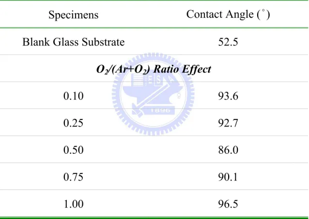
For the O2/(Ar+O2) ratio effect, the results of this study show that the deposition rate
decreased with an increasing O2/(Ar+O2) ratio. This was caused by a reduction in plasma
density due to the addition of electronegative oxygen. At an O2/(Ar+O2) ratio of ~0.3, XRD
results show that ZnO thin film forms a polycrystalline structure with the lowest FWHM (largest grain size). At the same time, the content fraction of the OⅠ
peak (O-Zn bond) and the corresponding binding energy reached their highest levels at this O2/(Ar+O2) ratio,
according to XPS analysis.
The smallest FWHM, largest grain size, and less relaxation stress were simultaneously created by annealing treatment. The moderation annealing temperature is an important factor for improving material properties such as film quality, stress, grain size, transmittance, and UV-shielding characteristics, etc. An annealing treatment below 300℃ offers significant
improvements, whereas it has no obvious variance when the annealing temperature exceeds 400℃. Finally, we deduced that the best annealing temperature is at 400℃ for glass substrate.
In summary, we have obtained the excellent properties of ZnO thin film on glass with the high transparency, good UV-shielding, and hydrophobic characteristics for glass industry applications. The final section of this thesis provides directions for future research on different deposition parameters (distance between target and substrate, working pressure effect, etc.).
Keywords: Zinc Oxide (ZnO), Sputtering, Langmuir probe, x-ray diffractometry (XRD),
誌謝
首先要感謝指導教授吳宗信教授對於學生在博士班期間的指導及協助,使得學生能 提昇自己各方面研究相關的能力以及國際視野,最後順利取得博士學位,在此表達最高 的敬意與謝意。此外,也要特別感謝魏大欽副教授在相關電漿理論及分析上耐心的教導 及指正,使得本研究能更加完整。而鄭宗杰助理教授從碩士班至博士班對於學生在生活 及研究上的提攜及建議不虞餘力,亦督促著學生不斷的成長,也致上衷心的謝意。最後, 同時也要感謝沈弘俊教授、溫志湧教授、傅武雄教授、陳慶耀教授、周長彬教授、魏大 欽副教授、鄭宗杰助理教授、謝健博士等口試委員對於論文中不盡完善的部分給予適當 的建議與指教,使本研究益加完備。 另外,也要感謝國家奈米元件實驗室(NDL)在實驗設備上的協助,當然也要特別感 謝材料分析組的工程師們的鼎力幫忙,包括楊君惠、沈奕伶、簡依玲、姚潔宜、郭美玲、 許瓊姿、周棟煥、林宏旻等。以及張妙如、簡秀芳等人在實驗過程中一般行政事務上的 協助,使學生在研究過程中遇到的疑難雜症均能順利解決並完成。其他包含黃文賢、黃 仕強、沈志彥、楊忠諺博士、謝健博士、張茂男博士、鄧建龍博士等人均在各種不同領 域上給予學生適當的建議及指教,使學生受益良多。還有目前已赴美攻讀博士的鄭明欣 學長,謝謝你的傾囊相授,讓我對材料分析開始有進一步的瞭解。最後當然也不能忘記 曾經在台南 NDL 內提供學生最多支援的工程師們,包括蔡來福、湯淵富、林育德、薛 漢鼎、文祥昇、陳永祥、陽永明等人,在此獻上最深的感謝。除此之外,在這段研究過程中一起打拼、相互砥礪、陪我度過這段有歡笑淚水過程 的謝盛祺、洪政男、蔡尚瑋、張原銘、溫華強等同學。以及無怨無悔被我壓榨的學弟妹 們(吳聲堯、毛穎恆、洪嘉良、廖士均、葉帝佑、鍾宛倩),因為有你們才能呈現如此完 整的成果。當然不能忘記還有現在任教於義守大學的簡賸瑞學長,感謝你們的陪伴及支 持。希望未來大家還可以一起打拼下去,加油! 然而,最重要的當然還有APPL 實驗室內所有學長姐、學弟妹們給予課業及生活上 的相互支持與砥礪,像是邵雲龍、梁桂雄、許國賢、李允民、周欣芸、鄭凱文、黃柏誠、 鍾東霖、陳立軒、梁偉豪、陳百彥、胡孟樺、鄭丞志,以及許多無法一一提及的學弟妹 們。其中要特別感謝邵董從碩班開始對我的照顧,除了提點我研究上要注意的所有細節 及方法外,對於生活上的瑣事及人際關係也給我許多的協助。當然也不能忘記一群人騎 腳踏車挑戰陽明山、東北角的事蹟,多虧這些驚人之舉,也讓求學生涯增添許多不可抹 滅的回憶,謝謝你們陪我度過這幾年充實的研究生活。 而家人給予我精神上、經濟上的支持與鼓勵,使得我在研究期間能夠無後顧之憂的 專心研究;此外,陪我度過這漫長研究生活的女友林欣儀,謝謝妳當我遇到低潮、不如 意時,適時給予我鼓勵並送上溫暖,且不辭辛勞的陪伴我跑遍各大大小小的國內、外研 討會,讓我能順利地完成學業。至於其他在身邊支持、鼓勵我的所有朋友們,雖然無法
一一提及各位,但也都給你們最深的祝福與感謝。在此將論文獻給你們,沒有你們的支 持就沒有現在的我。
許哲維 謹誌 2010.01.31. 于新竹·交通大學
Table of Contents
中文摘要
... i
Abstract ... iv
誌謝
... vii
Table of Contents ... x
List of Tables ... xiii
List of Figures ... xv
Nomenclature ... xxv
Chapter 1. Introduction ... 1
1.1 Background and Motivation ... 1
1.2 General Properties of Zinc Oxide (ZnO) ... 3
1.3 Deposition Techniques of ZnO Thin Films ... 4
1.4 Importance of Plasma Diagnostics ... 6
1.5 Specific Objectives of the Thesis ... 10
Chapter 2. Basics Theories ... 12
2.1. Thin Film Growth Mechanism ... 12
2.2. Fundamentals of Plasma Physics ... 15
2.3. Principle of Langmuir Probe Diagnostics ... 17
2.3.1. Introduction to I-V Curve ... 18
2.3.2. Theory of Langmuir Probe ... 21
2.3.2.1. Planar Probe with Collisionless Sheath ... 21
2.3.2.2. Cylindrical Probe with Collisionless Sheath ... 27
2.4. Theory of X-Ray Diffraction (XRD) ... 32
2.5. Theory of Optics ... 35
Chapter 3. Experimental Methods ... 38
3.1. Experimental Apparatus ... 38
3.1.1.1. RF Power Subsystem ... 38
3.1.1.2. The Magnetron Subsystem ... 39
3.1.1.3. The Temperature Control Subsystem ... 40
3.1.1.4. Mass Flow Control Subsystem ... 40
3.1.1.5. Pumping Subsystem ... 41
3.1.1.6. Pressure Control Subsystem and Gauge Meter Components ... 41
3.1.1.7. Target and Gases ... 43
3.2. Experimental Instrumentation ... 44
3.2.1. Plasma Diagnostics ... 44
3.2.1.1. Langmuir Probe System ... 44
3.2.2. Structural Characterization Techniques ... 46
3.2.2.1. Surface Profilometer (α-step) ... 46
3.2.2.2. X-Ray Diffractometry (XRD) ... 46
3.2.3. Chemical Characterization Techniques ... 48
3.2.3.1. X-ray Photoelectron Spectroscopy (XPS) ... 48
3.2.4. Optical Characterization Techniques ... 49
3.2.4.1. Ultraviolet-Visible Spectrophotometer (UV-VIS Spectrophotometer) ... 49
3.2.5. Hydrophobic/Hydrophilic Characterization Techniques ... 50
3.2.5.1. Contact Angle System ... 50
Chapter 4. Results and Discussion ... 51
4.1. Summary of Test Conditions ... 51
4.2. Plasma Characteristics ... 52
4.2.1. Effect of RF Power ... 52
4.2.2. Effect of Gas Ratio (Ar / O2) ... 57
4.3. Structural Characteristics ... 59
4.3.1. Effect of RF Power ... 59
4.3.2. Effect of Gas Ratio (Ar / O2) ... 62
4.4. Chemical Characteristics ... 64
4.4.1. Effect of RF Power ... 64
4.4.2. Effect of Gas Ratio (Ar / O2) ... 66
4.5. Optical Characteristics ... 67
4.5.1. Effect of RF Power ... 67
4.5.2. Effect of Gas Ratio (Ar / O2) ... 71
4.6. Hydrophobic/Hydrophilic Characteristics ... 74
4.6.1. Effect of RF Power ... 74
4.6.2. Effect of Gas Ratio (Ar / O2) ... 74
4.7. Annealing Temperature Effect of ZnO Thin Film ... 75
4.7.2. Optical Characteristics ... 79
Chapter 5. Summary and Recommendation of Future Works .... 81
5.1. Summary ... 81
5.2. Recommendation of Future Works ... 83
Appendices ... 86
Appendix A. Langmuir Probe Analysis... 86
References ... 89
List of Tables
Table 1.1. Key structural properties of zinc oxide (ZnO) ... 117
Table 1.2. Key optical properties of zinc oxide (ZnO) ... 118
Table 1.3. Key electrical properties of zinc oxide (ZnO) ... 119
Table 1.4. Key mechanical properties of zinc oxide (ZnO) ... 120
Table 2.1. Several inelastic collision types within the plasma [140-141] ... 121
Table 2.2. Approximation frequencies and vacuum wavelength ranges for various colors [153] ... 122
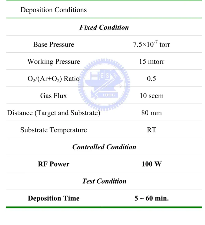
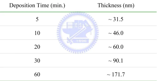
Table 4.1. The deposition conditions of ZnO thin films for thickness effect under a constant RF power ... 123
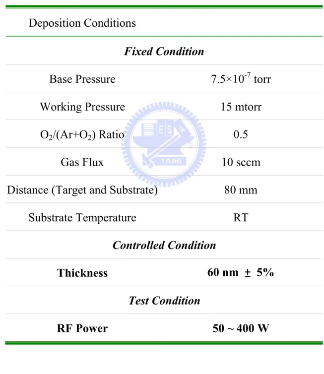
Table 4.2. The deposition conditions of ZnO thin films for RF power effect under a constant thickness ... 124
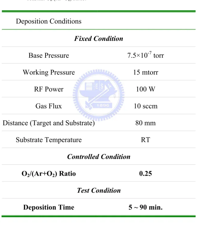
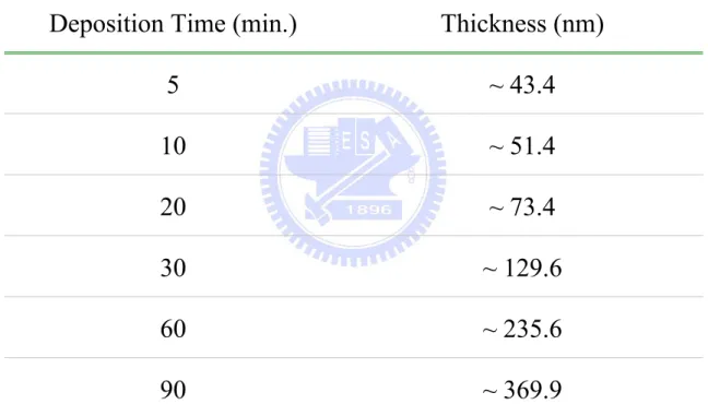
Table 4.3. The deposition conditions of ZnO thin films for thickness effect under a constant ... 125
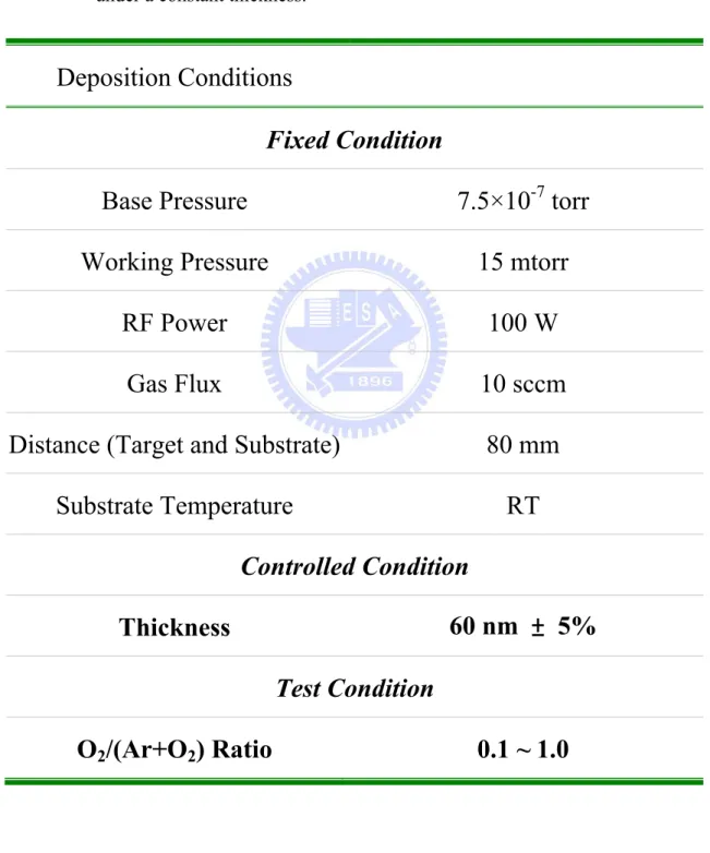
Table 4.4. The deposition conditions of ZnO thin films for ... 126
Table 4.5. Various thicknesses of ZnO thin films for ... 127
Table 4.6. Various thicknesses of ZnO thin films for ... 128
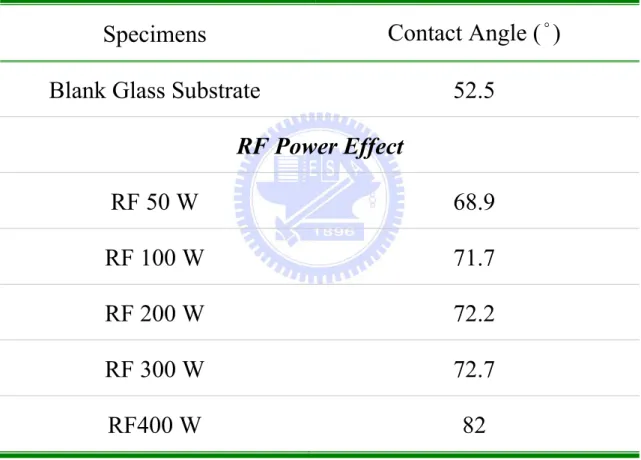
Table 4.7. Various contact angles of ZnO thin films for RF power effect under a constant thickness. ... 129
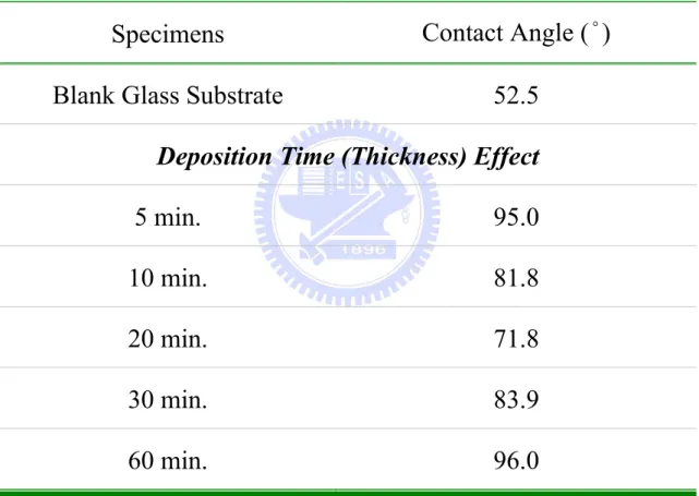
Table 4.8. Various contact angles of ZnO thin films for deposition time (thickness) effect under a constant RF power. ... 130 Table 4.9. Various contact angles of ZnO thin films for O2/(Ar+O2) ratio effect under a
constant thickness. ... 131 Table 4.10. Various contact angles of ZnO thin films for deposition time (thickness)
effect under a constant O2/(Ar+O2) ratio. ... 132
Table 4.11. The deposition conditions of ZnO thin films for annealing temperature effect under a constant thickness. ... 133 Table 4.12. Various lattice constants of ZnO thin films for annealing temperature effect
List of Figures
Figure 1.1. Hexagonal wurtzite structure of ZnO (small grey ball is zinc and big red ball is oxygen) [55]. ... 135 Figure 1.2. Hexagonal close-packed (HCP) structure of ZnO. ... 136 Figure 2.1. Schematic illustration of mechanism of thin film growth [136-137]. ... 137 Figure 2.2. Three different mechanisms for reactive sputter deposition: (a) at the target; (b)
in the plasma volume and (c) at the substrate [138]. ... 138 Figure 2.3. Several different electron-atom collisions: (a) ionization collision; (b)
excitation collision; (c) relaxation process and (d) dissociation process [140].139 Figure 2.3. Several different electron-atom collisions: (a) ionization collision; (b)
excitation collision; (c) relaxation process and (d) dissociation process [140]. (Continuous) ... 140 Figure 2.4. Paschen curve for a number of gases. (From A. von Engel, Ionized Gases.
Oxford University Press, Oxford, 1965. Reprinted with permission) [143] . 141 Figure 2.5. Schematic illustration of plasma diagnostic technique by using a Langmuir
probe. ... 142 Figure 2.6. Typical I-V characteristics for a Langmuir probe. ... 143
Figure 2.7. Theoretical shape of the saturation current portion of the probe characteristic for various probe shapes (planar, cylindrical and spherical) when the probe current is limited by orbital motions [119]. ... 144 Figure 2.8. Schematic illustration of sheath forms with different geometry of probes.145 Figure 2.9. The charge particles arrive to the plasma sheath by orbital motion. ... 146 Figure 2.10. Ion orbital motion within the plasma sheath of a cylindrical Langmuir probe
[141]. ... 147 Figure 2.11. Schematic diagram of Bragg diffraction from a set of parallel planes. 148 Figure 2.12. Schematic diagram of x-ray diffraction peak for calculating the grain size
(crystallite size) by Scherrer equation. ... 149 Figure 2.13. Reflection, propagation and transmission of a light beam incident on an
optical medium [152]. ... 150 Figure 2.14. The electromagnetic spectrum of radiation; the bandgaps and cutoff
frequencies for some optical materials are also shown [154]. ... 151 Figure 2.15. Interaction of photons with a material. In addition to reflection, absorption,
and transmission, the beam changes direction, or is refracted. The change in direction is given by the index of refraction n [154]. ... 152 Figure 3.1. The configuration of RF reactive magnetron sputtering system. ... 153 Figure 3.2. Schematic illustration of RF reactive magnetron sputtering system. ... 154
Figure 3.3. The configuration of RF power system. (a) Top and (b) front view of RF plasma generator system, respectively; (c) top and (d) side view of automatic
matching network system, respectively. ... 155
Figure 3.4. The configuration of Magnetron System. ... 156
Figure 3.5. The configuration of temperature controller system. ... 157
Figure 3.6. The configuration of mass flow controller (MFC) system... 157
Figure 3.7. The configuration of (a) mechanical pump and (b) cryogenic pump... 158
Figure 3.8. The configuration of MKS self-tuning controller. ... 158
Figure 3.9. The configuration of ionization & low vacuum gauge controller. ... 159
Figure 3.10. The configuration of Baratron capacitance manometer. ... 159
Figure 3.11. The configuration of thermocouple gauge. ... 160
Figure 3.12. The configuration of ion gauge. ... 160
Figure 3.13. The configuration of standard ESP analysis system with motorized Z-motion drive (Langmuir probe system). ... 161
Figure 3.14. Schematic illustrations of standard ESP analysis system with motorized Z-motion drive (Langmuir probe system). ... 162
Figure 3.15. Schematic illustration of construction of a cylindrical probe. (a) RF-compensated probe outline; (b) compensation electrode and probe tip detail; (c) probe tip assembly. ... 163
Figure 3.16. Schematic illustration of a RF-compensated probe for fixed installations and motorised Z-motion drives. ... 164 Figure 3.17. Schematic illustration of a typical automatic Z-motion driver. ... 164 Figure 3.18. The configuration of surface profilometer (Sloan Dektak 3030 profilometer).
... 165 Figure 3.19. The configuration of X'Pert PRO x-ray diffractometry (XRD). (Source by
PANalytical) ... 166 Figure 3.20. The configuration of goniometer of x-ray diffractometry (XRD). (Source by
PANalytical) ... 166 Figure 3.21. Schematic diagram of x-ray diffraction measured techniques: (a) Gonio scan
and (b) GIXRD scan. ... 167 Figure 3.22. The configuration of UV-VIS spectrophotometer. ... 168 Figure 3.23. The configuration of contact angle system. ... 168 Figure 4.1. Effect of deposition rate as a function of applied RF power at a constant
thickness of 60 nm. ... 169 Figure 4.2. The floating potential (Vf) and plasma potential (Vs) as a function of applied
RF power during ZnO thin film deposition. ... 170 Figure 4.3. The ion flux and ion bombardment energy (Vs-Vf) as a function of applied RF
Figure 4.4. The electron temperature (Te), electron number density (ne), and ion number density (ni) as a function of applied RF power during ZnO thin film deposition. ... 172 Figure 4.5. Relationship between ion flux and deposition rate as a function of applied RF
power during ZnO thin film deposition. ... 173 Figure 4.6. Effect of deposition rate as a function of O2/(Ar+O2) ratio under a constant
thickness of 60 nm. ... 174 Figure 4.7. XRD patterns of ZnO thin films as a function of deposition time (for thickness
effect) under a constant RF power of 100 W... 175 Figure 4.8. XRD patterns of ZnO thin films as a function of RF power (for power effect)
under a constant thickness of 60 nm. ... 176 Figure 4.9. Effect of grain size and FWHM as a function of RF power under a constant
thickness of 60 nm. ... 177 Figure 4.10. SEM image of ZnO thin films for various RF powers - (a) RF 50 W; (b) RF
100 W; (c) RF 200 W; (d) RF 300 W; (e) RF 400 W. ... 178 Figure 4.11. XRD patterns of ZnO thin films as a function of deposition time under a
constant O2/(Ar+O2) ratio of 0.25. ... 179
Figure 4.12. XRD patterns of ZnO thin films as a function of O2/(Ar+O2) ratio under a
Figure 4.13. Effect of grain size and FWHM of as a function of O2/(Ar+O2) ratio at a
constant thickness of 60 nm. ... 181 Figure 4.14. SEM image of ZnO thin films for various O2/(Ar+O2) ratios - (a) 0.10; (b)
0.25; (c) 0.30; (d) 0.50; (e) 0.75; (f) 1.00. ... 182 Figure 4.15. XPS survey spectrum of ZnO thin film. ... 183 Figure 4.16. The binding energy of (a) Zn 2p peak and (b) O 1s peak of ZnO thin film
from the XPS analysis. ... 184 Figure 4.17. The O 1s spectra (solid line), OⅠ
peak (dashed line) and OⅡ
peak (dot line) of XPS with various RF powers. ... 185 Figure 4.18. The O 1s spectra (solid line), OⅠ
peak (dashed line) and OⅡ
peak (dot line) of XPS with various O2/(Ar+O2) ratios. ... 186
Figure 4.19. The binding energy (●) and the content of OⅠ
peak (■) with various O2/(Ar+O2) ratios. ... 187
Figure 4.20. Transmittance spectra of pure ZnO thin films as a function of deposition time under a constant RF power of 100 W in (a) overall region and (b) UV region (280-400 nm). ... 188 Figure 4.21. Absorption spectra of pure ZnO thin films as a function of deposition time
under a constant RF power of 100 W in (a) overall region and (b) UV region (280-400 nm). ... 189
Figure 4.22. Transmittance spectra of pure ZnO thin films as a function of RF power under a constant thickness of 60 nm in (a) overall region and (b) UV region (280-400 nm). ... 190 Figure 4.23. Absorption spectra of pure ZnO thin films as a function of RF power under a
constant thickness of 60 nm in UV region (280-400 nm). ... 191 Figure 4.24. Transmittance spectra of ZnO/Glass as a function of deposition time under a
constant RF power of 100 W in (a) overall region and (b) UV region (280-400 nm). ... 192 Figure 4.25. Absorption spectra of ZnO/Glass as a function of deposition time under a
constant RF power of 100 W in UV region (280-400 nm). ... 193 Figure 4.26. Transmittance spectra of ZnO/Glass as a function of RF power under a
constant thickness of 60 nm in (a) overall region and (b) UV region (280-400 nm). ... 194 Figure 4.27. Absorption spectra of ZnO/Glass as a function of RF power under a constant
thickness of 60 nm in UV region (280-400 nm). ... 195 Figure 4.28. Transmittance spectra of pure ZnO thin films as a function of deposition
time under a constant O2/(Ar+O2) ratio of 0.25. ... 196
Figure 4.29. Absorption spectra of pure ZnO thin films as a function of deposition time under a constant O2/(Ar+O2) ratio of 0.25. ... 197
Figure 4.30. Transmittance spectra of pure ZnO thin films as a function of O2/(Ar+O2)
ratio under a constant thickness of 60 nm in (a) overall region and (b) UV region (280-400 nm). ... 198 Figure 4.31. Absorption spectra of pure ZnO thin films as a function of O2/(Ar+O2) ratio
under a constant thickness of 60 nm. ... 199 Figure 4.32. Transmittance spectra of ZnO/Glass as a function of deposition time under a
constant O2/(Ar+O2) ratio of 0.25. ... 200
Figure 4.33. Absorption spectra of ZnO/Glass as a function of deposition time under a constant O2/(Ar+O2) ratio of 0.25. ... 201
Figure 4.34. Transmittance spectra of ZnO/Glass as a function of O2/(Ar+O2) ratio under
a constant thickness of 60 nm. ... 202 Figure 4.35. Absorption spectra of ZnO/Glass as a function of O2/(Ar+O2) ratio under a
constant thickness of 60 nm in (a) overall region and (b) UV region (280-400 nm). ... 203 Figure 4.36. Contact angle image of blank glass substrate. ... 204 Figure 4.37. Contact angle images of ZnO thin Films under a constant thickness for
various RF powers - (a) RF 50 W; (b) RF 100 W; (c) RF 200 W; (d) RF 300 W; (e) RF 400 W. ... 205
Figure 4.38. Contact angle images of ZnO thin Films under a constant RF power for various deposition time - (a) 5 min.; (b) 10 min.; (c) 20 min.; (d) 30 min.; (e) 60 min. ... 206 Figure 4.39. Contact angle images of ZnO thin Films under a constant thickness for
various O2/(Ar+O2) ratio - (a) 0.10; (b) 0.25; (c) 0.50; (d) 0.75; (e) 1.00. .... 207
Figure 4.40. Contact angle images of ZnO thin Films under a constant O2/(Ar+O2) ratio
for various deposition time - (a) 5 min.; (b) 10 min.; (c) 20 min.; (d) 30 min.; (e) 60 min; (f) 90 min. ... 208 Figure 4.41. XRD patterns of ZnO (0002) orientations as a function of annealing
temperature is shown by (a) separation and (b) overlap way. ... 209 Figure 4.42. The ZnO (0002) diffraction peak shifted as a function of annealing
temperature. ... 210 Figure 4.43. Effect of grain size and FWHM as a function of annealing temperature.211 Figure 4.44. Transmittance spectra of pure ZnO thin films as a function of annealing
temperature in (a) overall region and (b) near UV edge. ... 212 Figure A.1. Step 1 – I-V curve raw data by Langmuir Probe. ... 213 Figure A.2. Step 2 – (a) I2-V curve and (b) a ion current linear regression fit is fitted in the
ion saturation. ... 214 Figure A.3. Step 3 – the square root of fitted line to I2-V curve in ion saturation. .... 215
Figure A.4. Step 4 – the electron I-V curve which consists of an electron current component only. ... 216 Figure A.5. Step 5 – the natural logarithm of electron current (ln(Ie)) versus probe
potential from the electron I-V curve. ... 217 Figure A.6. Step 6 – the 1st derivative of Ie-V curve. ... 218
Figure A.7. Step 7 – the 2nd derivative of Ie-V curve. ... 219
Nomenclature
a Probe Radius
Abs Absorption
ave
Abs Average Absorption
ZnO
Abs Absorption of ZnO /
ZnO Glass
Abs Absorption of ZnO on Glass
S
A Sheath Area
P
A Probe Area
B Full Width at Half Maximum (FWHM)
m
B Bulk Modulus 0
c The Speed of Light in Vacuum
c The Speed of Light in Free Space
p
C Specific Heat
d Interplanar (Lattice) Spacing
P
d Probe Length
t
d The Thickness of Material
e Elementary Charge; e = 1.602×10⁻¹⁹ Coulomb (1 coulomb = 6.24×10¹⁸)
E Energy of Light
b
coh E Cohesive Bandgap g E Energy Bandgap Y E Young’s Modulus F Potential Function E
f Electron Energy Distribution as a Function of Probe Voltage
i
f Ionicity
h Planck’s Constant; h = 6.62×10⁻³⁴ J·s
H Hardness
K Boltzmann Constant; K = 1.38 × 10⁻²³ J/K
k Constant Dependent on Crystallite Shape 0
I The Intensity of Incident Light
a
I The Portion Absorbed of the Incident Light
e
I Electron Current ,
e Sat
I Electron Saturation Current
i
I Ion Current ,
i Sat
I Ion Saturation Current
P
I Probe Current
r
I The Portion Reflected of the Incident Light
t
r
J Particle Current Density
M Mass
e
M Electron Mass
i
M Ion Mass
N Particle Number Density
n Refractive Index
e
n Electron Number Density
es
n Electron Number Density of Sheath
i
n Ion Number Density
is
n Ion Number Density at Sheath
P
n Plasma Number Density
s
n Number Density at Sheath
P Impact Parameter
R Reflection
S Plasma Sheath Radius
I S Incident Beam S S Scattered Beam t S Sheath Thickness % T Transmittance
% ave T Average Transmittance e T Electron Temperature % ZnO T Transmittance of ZnO / % ZnO Glass
T Transmittance of ZnO on Glass
B
u
Bohm Velocityf
V Floating Potential
S
V Plasma Potential (Space Potential)
P
V Probe Potential
S f
V −V Ion Bombardment Energy
α Absorption Coefficient
a
α Thermal Expansion Coefficient in a-axis
c
α Thermal Expansion Coefficient in c-axis 0
ε Static Dielectric Constant
ε∞ High Frequency Dielectric Constant
c
κ Thermal Conductivity
υ The Speed of Light in the Material
ν The Frequency of Light
a
v Charge Particle Velocity to Arrive Probe Surface
S
p
v Charge Particle Velocity in Plasma
r
v Radial Velocity
vφ Azimuthal Velocity
v
Mean Speed in Thermal Equilibrium
D
λ Debye Length
L
λ Wavelength of Light
M
λ Mean Free Path
r
λ Wavelength of Radiation
n
μ Hall Mobility for n-type
p
μ Hall Mobility for p-type
B
Chapter 1. Introduction
1.1 Background and MotivationNanotechnology has attracted great attention over the past several decades due to the increasing emphasis on convenience, as evidenced in product innovations such as the downscaling of product size, weight reduction, improvement in the operation efficiency of components and decreased costs, etc. In light of this, material science has become more prominent, as it distinguishes the widely varying properties of a material between its macro scale and micro scale. Within this setting, many researchers have investigated the phenomena of various materials in the micro or nano scale and how they apply to various industries [1], such as optoelectronics, mechanical devices, communication, display technology, energy & environment, etc.
Among these research fields, Zinc Oxide (ZnO) is one of the promising candidate materials, and has been extensively investigated for various applications in many fields, including optoelectronics (e.g. light emitting diode (LED) [2-4], laser diodes (LDs) [5], field emission displays (FEDs) [6-7], flat panel displays (FPDs) [7-8], transparent conductive oxides (TCOs) [9-10], solar cells or photovoltaic devices [11-13], photocatalysis [14], and optical waveguides [15]), piezoelectric applications [16-19] (e.g., surface acoustic waves (SAWs) [20], bulk acoustic waves (BAWs) [21], and transducers [22]), sensors [23] (e.g. ultraviolet (UV) detectors [24], photodetector [25],
gas sensor [26]), and glass industry (e.g. heat-reflecting coating [27], architectural windows [28-33]), etc.
Broad applications of ZnO thin film arise from several unique material properties, including a hexagonal wurtzite structure and wide direct band gap at room temperature (RT) which is larger than GaN. In addition, it also exhibits highly efficient UV emission properties resulting from a high exciton binding energy level of 60 meV at RT, which leads to extreme stability of excitons and enables devices to work at a low threshold voltage for optical devices. Furthermore, due to its simultaneously high conductance, high melting point (1975℃), chemical and thermal stability, and high piezoelectric coupling coefficient, ZnO is also an important piezoelectric material for piezoelectric or electronic devices. Additional advantages of ZnO are that [34] (1) it consists of cheap, abundant and non-toxic elements, it can replace tin-doped indium oxide (ITO) elements, (2) it can be coated over a large area; (3) it allows adjusting of the UV absorption or bandgap by doping impurity; (4) it can tolerate reducing chemical environments in a hydrogen plasma [35] because of its high stability; and (5) it can be deposited at a low temperature with different techniques, which allows its growth on flexible substrates for better TCO films. Incidentally, many researchers addresses diverse nanostructures of ZnO [36-37], including one-dimension (such as nanowires [2, 6, 10, 18-19, 38-44], nanotubes [45], nanorods [7, 46-47], nanorings [48], nanocoils [49], nanobelts [50-51],
nanotips [23], nanoneedles [14], etc.), two-dimension (like as thin film [12-14, 52]) and three-dimension (bulk material in general), respectively. It is because of these qualities that ZnO is one of the most interesting semiconductors of II–VI compounds, and maintains broad and significant scientific and technological importance.
1.2 General Properties of Zinc Oxide (ZnO)
ZnO is a hexagonal wurtzite structure with 6mm point group symmetry, space group #186 P63mc ( 4
6v
C ) [53-54] as shown in Fig. 1.1 [55]. According to the Bravais lattice, ZnO is also a hexagonal close-packed (HCP) lattice that is composed of two interpenetrating HCP sublattices of cation (Zn) and anion (O), displayed by the length of the cation-anion bond in the c-direction (see Fig. 1.2). The lattice constants of ZnO structure are a1 = a2 = a3 = 3.250 Å and c = 5.207 Å [35, 55], respectively. ZnO is a
compound whose two elements have different ion radii, and the ratio of c-direction to a-direction (c/a) in ZnO is about 1.602. The c/a ratio is slightly smaller than the ideal HCP structure (1.633). The zinc and oxygen crystal surfaces are quite different with regard to their surface energies, deposition rate, etc. The zinc surface has a higher surface energy and faster deposition rate than the oxygen surface. Also, the zinc surface’s faster deposition rate causes it to form a steeply inclined pyramidal face [20]. Because of the minimizing surface energy will exhibit on the top surface during the evolution of crystalline morphology. Hence, ZnO tends to grow along the c-axis
orientation normal to substrate, with the crystallographic plane of the lowest free energy parallel to the substrate.
ZnO is also a direct wide bandgap of Ⅱ-Ⅳ semiconductors. Its energy gap is 3.2 eV at RT and 3.44 eV at 4.2 K [56], but its optical bandgap is close to 3.37 eV (300 K; RT) by measuring on the thin film. ZnO films have higher transparency in the visible region because ZnO’s optical bandgap is larger than the energy of a visible light wave. The light wavelength of emission of ZnO displays the UV emission (about 370 nm) [57-58]. In addition, it exhibits highly efficient UV emission properties resulting from a large exciton binding energy of 60 meV at RT, which is much larger than other materials such as GaN (28 meV) and ZnSe (19 meV), etc. Based on above advantages, ZnO is also a wonderful piezoelectric material for piezoelectric or electronic devices. For this reason, ZnO remains one of the most interesting semiconductors of II–VI compounds, with many researchers investigating its detail characteristics further. We have organized and summarized several properties of ZnO films list in Table 1.1 to
Table 1.4 [4, 35, 37, 59-72].
1.3 Deposition Techniques of ZnO Thin Films
The morphology, structural properties, and physical properties of ZnO thin films depend heavily on deposition conditions and techniques. ZnO thin films have been grown by various deposition methods, such as sputtering [3, 8, 12, 24, 73-89],
metal-organic chemical vapor deposition (MOCVD) [14, 90], molecular beam epitaxy (MBE) [91], plasma enhanced chemical vapor deposition (PECVD) [92], atomic layer deposition (ALD) [93], atomic layer epitaxy (ALE) [94], pulsed laser deposition (PLD) [44, 52, 95-96], chemical bath deposition [97], sol-gel process [43, 98], spray pyrolysis [99], ion beam deposition [100], filtered cathodic vacuum arc technique [32], and vapor phase epitaxy (VPE) [101]. Out of these, the sputtering method is one of the simplest ones that can be used to obtain higher thin film quality (orientation and uniformity) with low growth temperature and even amorphous substrate. Consequently, the mobility of sputtered species on the leading surface is enhanced and the crystallinity is higher at low substrate temperatures. Recently, the radio-frequency (RF) sputtering technique has been developed to insulate oxide films through reactive sputtering and large area deposition. The RF technology exhibits several important advantages of the deposition
of oxide films over the conventional DC reactive magnetron sputtering. For instance, it can minimize arcing and improve the properties of films, such as high transparency and conductivity with smooth surface, high deposition rate, high quality, and insulation from oxide material deposition.
In addition, magnetron sputtering offers the important advantage of high density plasma for thin film deposition. Magnetron sputtering produced the magnetic and electric fields to confine the secondary electrons of the plasma in front of the cathode
(target). Because the electrons are significantly influenced by the magnetic field, the high ionization efficiency is achieved. This phenomenon causes the formation of high density plasma when the ionization probability increased. High deposition rate, reduced working pressure, good adhesion of film on the substrate, low substrate temperature, high density of the films and scalability to large areas are additional advantages of magnetron sputtering. Due to the above advantages, RF reactive magnetron sputtering was used in this study.
1.4 Importance of Plasma Diagnostics
To interpret the influencing factors of a material, it is imperative to understand the inextricable relationship between deposition conditions and techniques, and the characteristics of microstructures, as described above. Generally speaking, in this study the deposition conditions of sputtering method involve power source (DC, RF), substrate temperature, working pressure, gas flux, gas type (gas ratio), distance between the target and the substrate, substrate rotation, target and substrate types, etc. Unfortunately, all of above deposition conditions affect the plasma characteristics during deposition process. This is because the sputtering technique is based on the plasma. However, the plasma status plays a key role in linking the relationship between the plasma characteristics and the physical properties of the material.
Plasma has taken on increasingly extensive application over the past few decades. In addition to being important in many aspects of our daily lives, plasma is estimated to constitute more than 99 percent of the visible universe [102]. As a result, plasma physics has become one of the major research fields of physics. Understanding the phenomena of plasma permits standard techniques to be applied and interpreted correctly, and also forms the basis of innovation.
Plasma parameters of sputtering process are important conditions to influence both in the deposition processes and investigation of ZnO thin film properties. Therefore, researchers have developed and designed several diagnostics techniques to measure and analyze the plasma during the sputtering. There are various techniques to group diagnostics when studying plasma physics. First, one might divide plasma diagnostics into two possible categories: one is plasma parameter measurements, including the measurement of plasma number density, plasma temperature, plasma potential, and so on; the other one is experimental technique—that which can be learned using several measuring instruments, such as a detector or spectrometer. Therefore, the standard categorization of plasma diagnostics should include classification by magnetic measurement, plasma particle flux measurement, plasma refractive index, electromagnetic emission from free electrons, electromagnetic emission from bound electrons, scattering of electromagnetic wave, natural atom diagnostics, and fast ions
and fusion products [103]. Diagnostic techniques could also be generally divided into
invasive and non-invasive techniques. Microwave diagnostics and optical methods
involve non-invasive techniques, like optical emission spectroscopy (OES) [81], laser-induced fluorescence (LIF) [104], laser interferometer [105], or absorption spectroscopy [106], etc. All of these methods generally measure the entire averaged properties of the plasma. On the other hand, the locally plasma diagnostics can be determined by invasive techniques, such as an energy resolved mass spectrometer [107], Langmuir probe [81-85, 104, 107-110] and emissive probe [104]. Although invasive techniques yielded locally plasma characteristics, they also made local perturbation in the plasma. Nonetheless, it is typically a good diagnostics method/tool for investigating plasma phenomena.
Among invasive techniques, the electrostatic probe is the primary technique for measuring the characteristics of plasma. This technique was developed by Langmuir and Mott-Smith [111-117] as early as 1924, and is called Langmuir probe. Based on the electrostatic probe, it consists of a small metallic wire electrode that is immersed into the plasma. The probe is swept a voltage from negative to positive by the external power supply, and is collected the feedback current of inside plasma through the small metallic wire electrode. Based on this characteristic of I-V curve, the detail theory has
been gathered and developed by many scientists [118-124], including F. F. Chen, L. Schott, N. Hershkowitz, etc.
In 1930, Druyvesteyn [125-126] successfully demonstrated that any type of electron energy distribution function (EEDF) could be directly received by the secondary differential of the I-V curve of the probe. Fortunately, the electron energy
distribution probability could also be estimated directly by the plasma characteristics. In addition, many scientists [127-128] have demonstrated that the electron velocity distribution does not completely follow the Maxwellian velocity distribution and is not isotropic, especially as demonstrated in low pressure and partial ionization of plasma in 1950s. Johnson and Malter [129-130] developed and designed the double probe in 1949 and Yamamoto [131-132] improved this design to triple probe in 1960. The triple probe measurement coupled the single and double probe measurement to replace the sweeping bias techniques. The development of the above probes led to more selectivity in plasma diagnostics technologies, and more comprehensive applications. To determine plasma characteristics precisely, it is important that the cylindrical and spherical probe be used. For this reason, Laframboise [133] studied the theory of cylindrical and spherical probe. Subsequent scholars frequently quote his results when discussing the investigation and application of the probe. In combination with their contributions, the Langmuir probe and technques can perform a complete analysis on various modules and theories.
The Langmuir probe has been widely used to understand the plasma physics and phenomena since 1924. Several key plasma characteristics can be acquired based on this technique, including floating potential (Vf), plasma potential (Vs), electron temperature
(Te), electron number density (ne), and ion number density (ni), etc. These fundamental
plasma characteristics helped us interpret plasma status during sputtering processes and linked the relationship between the plasma characteristics and general physics properties (such as structural, electrical, optical, and chemical, etc.) during thin film growth. At this point, it is an important technology and it helpful to obtain and control the optimal plasma status for enhancing film quality and reproducibility.
1.5 Specific Objectives of the Thesis
Since material properties strongly affect the performance of a device, understanding the influence of deposition conditions with material properties is very important. Many studies have focused on the transmittance of the visible and enhanced hydrophobic characteristics of ZnO film, while almost none have paid attention to simultaneous characteristics of high transmittance in the visible, high absorbance in the UV region, and self-clean capability, which is very important for applications in the glass industry [28]. In this thesis, we have focused on investigating the ZnO thin film effects of RF power, O2/(Ar+O2) ratio, annealing temperature, and film thickness on the
plasma conditions and general physical properties (including structural, optical, and chemical properties) of ZnO thin films. Then we address the construction and diagnosis of the plasma properties of the system, with the objective of simplifying plasma diagnostics in the future.
The organization of the thesis is as follows: it begins by introducing the development and application of II–VI compounds semiconductors of ZnO material; several fundamental principles are then expounded carefully in Chapter 2, including thin film growth mechanism, plasma diagnostics theories, X-ray diffraction and optics principles; the experimental apparatus and measurement methods are described briefly in Chapter 3; the results and discussion are organized and analyzed by theories and experimental data in Chapter 4; Chapter 5 reports the final summary of this thesis and recommendations for future work.
Chapter 2. Basics Theories
2.1. Thin Film Growth MechanismUnderstanding the thin film growth mechanism is important to interpret the difference between materials by different deposition conditions or techniques. Consequently, brief descriptions of the thin film growth mechanism and deposition processes are contained in the following section. There are three main steps that occur in any thin film growth mechanism: (1) production of the appropriate atomic, molecular, or ionic species; (2) transport of these species to the substrate through a medium; and (3) condensation on the substrate, either directly or via a chemical and/or electrochemical reaction, to form a solid deposit [72, 134]. Figure 2.1 reveals the general scheme of the thin film growth mechanism [72, 135-137], which occurs as follows:
(a) The species (atomic, molecular, or ionic) lose their velocity component normal to the substrate when they are impacting the substrate. This phenomenon causes them to be physically adsorbed on the substrate surface.
(b) The adsorbed species migrate to equilibrium position on the substrate surface because of they are in non-thermal equilibrium with substrate at the initial stage. The bigger clusters are forming by their interaction among themselves in this process.
(c) In general, the clusters are also called the “nuclei”. The nuclei are not thermodynamically stable, and depend on the deposition parameters to desorb from the surface in time. If the cluster collides with other absorbed species before desorbing, the size of nuclei gradually grows.
(d) Next, once the cluster reaches a certain critical size, it overcomes the nucleation barrier and becomes thermodynamically stable. The stable chemisorbed and critical-size nuclei are forming in this stage, which is called the nucleation stage.
(e) The critical nuclei are growing in number and in size until the saturation nucleation density is reached. The number of parameters strongly influences the nucleation density and the average nucleus size, such as the energy of the impinging species, the activation energies of adsorption, thermal diffusion, etc. (f) A nucleus can grow both parallel and perpendicular to the substrate by surface
diffusion of the adsorbed species and the direct impingement of the incident species, respectively. However, the grown nuclei are called islands.
(g) The coalescence stage is the stage of thin film formation. The small islands start coalescing with each other to form bigger islands and reducing the surface area, which is a process called agglomeration. Increasing the surface mobility of the adsorbed species can be enhancing the phenomenon of agglomeration. (h) The originally thin film structure must undergo the cluster, nucleation, island
growth, and coalescence stage. Finally, the thin film structure will reach complete formation in this stage through structural changes from discontinuous islands, porous network type and filling of the channels and holes, resulting in a completely continuous thin film.
Incidentally, the reactive sputtering can also deposit the oxide, nitride and sulfide thin films in a chamber consisting of reactive gas mixed with inert gas. The target of ceramic or metal is able to form these compound thin films. Figure 2.2 illustrates how Holland [138] deduced three possible formation processes in which active gas could combine with metal to form a sputtered gas-metal film. These are (1) at the surface of the target; (2) in the space between the target and the substrate; (3) on the surface of the substrate. Im et al. [139] also found similar phenomena in their work with different oxygen pressures during the PLD process.
2.2. Fundamentals of Plasma Physics
Plasma science [112-122, 133, 137-138, 140-147] began in the 1920s with experiments on gas discharges by such noted scientists as Irving Langmuir [118]. Plasma, which is a partially ionized gas consisting of equal numbers of positive and negative charges and a different number of unionized neutral molecules, is also called a “Fourth State of Matter.” More precisely, plasma is a quasi-neutral gas of charged and neutral particles that exhibits collective behavior [137, 140]. In general, laboratory plasma is a weakly ionized plasma discharge, which displays the following qualities: (1) they are driven electrically; (2) they depend on charged particle collisions with neutral gas molecules; (3) there are boundaries at which surface losses are important; (4) ionization of neutrals sustains the plasma in the steady state; and (5) the electrons are not in thermal equilibrium with the ions [141]. An external energy source—such as direct current (DC), alternating current (AC), radio frequency (RF) or microwave (MW) power generator—must supply enough power to ionize and maintain the plasma.
Understanding the phenomenon inside plasma, especially the phenomenon of collisions, is very important to maintaining the plasma. Elastic collisions and inelastic collisions are two kinds of collisions inside plasma. Elastic collisions do not involve energy exchange between the colliding particles, but they are not important to maintain the plasma. Nevertheless, inelastic collisions are significant because there are many
inelastic collisions happening simultaneously in the plasma. This includes collisions between electrons and neutrals, between ions and neutrals, between ions and ions, and between electrons and ions, etc. The following section will describe several critical inelastic collisions, as illustrated in Table 2.1 and Fig. 2.3 [118, 140-141].
In collision ionization, one free electron transfers a portion of its energy to the orbital electron when the free electron collides with an atom or a molecule. When an orbital electron obtains enough energy to leave its orbit and the confinement of the nucleus, it becomes a free electron. This process is called electron-impact ionization by collision. But not every collision generates enough energy for ionization. If the collision provides the orbital electron just enough energy to jump to a higher energy level of orbit, this process is called excitation collision. Nonetheless, this higher energy level of orbit is only stable for a short lifetime. The electron will fall back to the lowest energy level or ground state. This process is called relaxation collision. According to conservation of energy, the excited atom or molecule relaxes to its ground state and releases the extra energy in another form, such as a light emission (photons). When an electron collides with a molecule, the energy is higher than the molecule bonding energy which a molecule breaks the chemical bond causes the free radicals generated. This process is called dissociation collision.
According to Paschen’s Law, a plasma discharge can occur only if free electrons accelerated by an electric field gain enough energy between successive collisions with neutral atoms (or molecules) to ionize the atoms. Ionization releases an additional electron which also accelerates, collides with atoms, and causes more ionization. The resulting avalanche leads to a discharge. This behavior is represented by the familiar Paschen curve as shown in Fig. 2.4 [142-143]. The minimum in this curve occurs at the condition where the electronic mean free path is just barely sufficient to allow electrons to gain the ionization energy that the plasma will be generating.
2.3. Principle of Langmuir Probe Diagnostics
A metal probe is one of the earliest and still most useful tools for diagnosing plasma characteristics inside plasma. Metal probes are often used in plasma diagnostics because they are simple and easily constructed. Researchers acquire the electron or ion current, gauging their bias voltage with respect to the plasma potential, while the metal probe inserted into the plasma. Because these probes are quite small, they produce only minor local perturbations of the plasma. Although probes upset local surroundings of plasma, they can still determine electron temperature (Te), electron number density (ne),
ion number density (ni), floating potential (Vf), and plasma potential (Vs) over an
extremely wide range of parameters. These metal probes are usually called Langmuir Probe, which were introduced by Langmuir and analyzed in considerable detail by
Mott-Smith and Langmuir (1926) [141]. It is extraordinary that one type of diagnostic, Langmuir probe, has been used to serve the full range of diagnostic roles over such a wide range of plasma densities. Across a broad spectrum of situations, the details of current-voltage (I-V) characteristics can be related to the plasma parameters. The
voltage and current of a probe defined in Fig. 2.5 leads to a typical probe I-V
characteristic as shown in Fig. 2.6.
2.3.1. Introduction to I-V Curve
In order to obtain the I-V curve, the probe bias is swept from negative voltage to
positive voltage with respect to the ground. Electrons and ions are either attracted or repelled and net current is collected by the probe bias changes. According to this I-V
curve, several plasma characteristics are acquired, including plasma number density (ne,
ni), plasma temperature (Te), plasma potential (Vf, Vs) and electron energy distribution
function (EEDF), respectively. A typical I-V curve can be divided into three regions and
two meaningful potential value points [119-122], including: (1) ion saturation region:
VP < Vf ; (2) transition region: Vf < VP < Vs; (3) electron saturation region: Vs > VP; (4)
floating potential: VP = Vf ; and (5) plasma potential: VP = Vs, respectively. It should be
noted that the measuring current that the probe collects is the summation of the electron current and the ion current, and the magnitude of the ion saturation current is much smaller than the electron current due to its much greater ion mass.
1. Ion saturation Region.
Before measuring the plasma, the probe bias provides a negative voltage to the probe in order to reduce or avoid perturbation of the plasma. The plasma measurement process proceeds until the potential equals the floating potential, which is called the ion saturation region. This is because the main probe bias is negative, causing it to attract most ions or repel most electrons. In the other hands, the number of collective ions is tending saturate state with negative bias increasing. Although many ions can be collected by the Langmuir probe, some cannot. According to the Bohm criterion, the velocity of ions should be accelerated over the Bohm velocity to collect the ion [119, 141, 144]. The Bohm velocity is given by:
1/2 e B KT u M ⎛ ⎞ = ⎜⎝ ⎟⎠ (2.1) 2. Transition Region
The I-V curve increases exponentially from the floating potential, then continues
until to the plasma potential when none of the electrons are repelled by a negative potential, which is called the transition region. Otherwise, electrons are repelled according to the Boltzmann relation until they reach the floating potential. In this region, the electron temperature can be estimated by the slope of the (lnI)-V curve. It is a good
3. Electron Saturation Region
For increasing the probe bias over the plasma potential, the number of collective electrons tends to saturate with positive bias increasing, but almost no ions can be collected in the electron saturation region. The electron sheath form in the probe surface and the electron current is limited by the thermal motion of electrons arriving to the sheath. The thickness of the sheath would increase with the raising potential in a non-planar probe. The electron saturation current might be a constant in the planar probe, but it is not always a constant, and increases with the raising probe potential in the cylindrical and spherical probes. Figure 2.7 presents the various I-V curve forms in
three different probes: planar, cylindrical and spherical probes, respectively [119]. 4. Floating Potential (Vf)
When the total collective current of a negative electron and positive ion is equal to zero, I = 0, meaning the net current is zero. The point at this moment is called floating
potential. The floating potential is sometimes considered to be the ground. 5. Plasma Potential (Vs)
When the probe bias is equal to plasma potential (VP = Vs), the probe and plasma
are at the same level. The plasma potential is also called space potential. In this potential, the more mobile electron contributes the main electron because of the positive
current flowing from the probe into the plasma at this moment. If the probe bias is increased over the plasma potential, the saturation of currents will lead electron saturation. This region is called electron satruaion region.
2.3.2. Theory of Langmuir Probe
The probe is immersed in the plasma through Langmuir probe. Although its structure is simple, its theory is quite complicated. In order to simplify the probe theory, we must make the following assumptions:
1. The plasma should be uniform and quasi-neutral in the condition without the probe.
2. Electrons and ions must obey Maxwellian velocity distribution. 3. Electron temperature is far higher than ion temperature.
4. The mean free path of electron and ion is far larger than any characteristic length. This means the collisionless is near from the probe.
5. Each charged particle hitting the surface of probe will be neutralized completely and secondary electrons will not occur.
2.3.2.1. Planar Probe with Collisionless Sheath
Based on the basic assumptions above, the probe is immersed in the plasma. The plasma sheath of planar probe is still a plate (one-dimension) due to the geometry of
probe. The plasma sheaths of the cylindrical and spherical probes are two-dimensional and three-dimensional, respectively. Figure 2.8 reveals the different sheath forms with various geometry of probe. Consider a planar probe with the physics probe area AP>> St,
where St is the sheath thickness, such that the collecting area AP is essentially
independent of St. This probe allows the effective collection area of probe AS to equal
the collection area of probe AP.
In the next two sections, we will discuss electron current and ion current. The first part will focus on electron current. According to the gas dynamics theory, in the thermal equilibrium plasma without perturbation, the particle current density is written by:
r
1 J N v
4
= (2.2) where Jr is particle current density, N is particle number density, and v is mean speed
in thermal equilibrium, also given by:
1/2 8KT v M π ⎡ ⎤ = ⎢⎣ ⎥⎦ (2.3) Then the electron current Ie can be expressed:
1 1
4 4
e e S e e P e
I = en A v ≈ en A v (2.4) In the electron saturation region, VP ≥ Vs, all electrons move into the sheath with
thermal equilibrium motion. It causes the electron current to reach saturation state. It can be assumed that the plasma is quasi-natural plasma at the sheath edge, i.e.
e i
n∞ ≈n∞ ≡n∞ (2.5) where the number density of electrons, ions and plasma with infinity distance from the probe in the plasma is represented by ne∞, ni∞, and n∞, respectively.
According to Eq. (2.5), the electron saturation current can be rewritten: , .
1 1
4 4
e Sat e P e P e
I = en A v∞ ≈ en A v∞ (2.6) Electrons are repelled by the probe in the ion saturation region and transition region (VP < Vs). Based on previous assumption, electrons and ions must obey the
Maxwellian velocity distribution as
( )
1 2 2 1 2 2 exp e e e e e e e M v KT f v n M KT π ∞ ⎛ ⎞ ⎛ ⎞ ⎜ ⎟ = ⎜ ⎟ ⎜ ⎟ ⎝ ⎠ ⎝ ⎠ (2.7) From the Boltzmann relation, the electron number density becomes:(
)
exp P S e e e e V V n n KT ∞ − ⎡ ⎤ = ⎢ ⎥ ⎣ ⎦ (2.8)Therefore, the electron current in the transition region and ion saturation region can be represented as
(
)
(
)
, . 1 exp exp 4 P S P S e P e e Sat e e e V V e V V I en A v I KT KT ∞ − − ⎡ ⎤ ⎡ ⎤ = ⎢ ⎥ ⎢ ⎥ ⎣ ⎦ ⎣ ⎦ = (2.9)Finally, a summary of the electron current derived above is listed as following: (a). The electron current in electron saturation region: Ie =Ie Sat, .
(b). The electron current in transition region: , .exp
(
P S)
e e Sat e e V V I I KT − ⎡ ⎤ = ⎢ ⎥ ⎣ ⎦(c). The electron current in ion saturation region: , .exp
(
P S)
e e Sat e e V V I I KT − ⎡ ⎤ = ⎢ ⎥ ⎣ ⎦Now we will focus on the ion current. Ions are attracted by the probe during VP <
Vs. The analysis of ion current is more complicated than for electron current. This is
because ions possess lower temperature, larger mass and far smaller thermal average velocity in thermal equilibrium than electrons. Hence, the Bohm criterion on the ion sheath must be discussed first.
The ion sheath is formatted near the probe surface when the probe potential is lower than plasma. The electron number density would decay to shield the electrons from the wall. We deduce that a transition layer or presheath must exist between the neutral plasma and non-neutral sheath in order to maintain the continuity of ion flux, giving rise to an ion velocity at the plasma-sheath edge.
We define the reference electric potential as plasma potential (Vs) and only minor
potential difference in the presheath. In addition, the interface between plasma sheath and presheath maintains the assumption of quasi-neutral plasma. Let the ion temperature be zero, based on the cold plasma state. This means the ions are almost stationary with infinity distance from the probe in the plasma.
![Table 2.2. Approximation frequencies and vacuum wavelength ranges for various colors [153]](https://thumb-ap.123doks.com/thumbv2/9libinfo/8244086.171440/153.892.167.809.435.829/table-approximation-frequencies-vacuum-wavelength-ranges-various-colors.webp)