Tungsten on Aluminum with a Vapor Phase
Precleaning Technology
Kow-Ming Chang, Ta-Hsun Yeh, Shih-Wei Wang, and Chii-Horng Li
Departmentof Electronics Engineering and Institute of Electronics, National Chiao Tung University and National Nano Device Laboratory, Hsinchu, Taiwan
ABSTRACT
A simple and efficient precleaning of an aluminum surface with hydrochloric acid vapor prior to selective chemical vapor deposition of tungsten was investigated. The vapor phase precleaning was shown to remove the aluminum native oxide as well as reduce the aluminum fluorides formed at the W/AI interface during initial reaction of WF6 with the alu-minum underlayer. It was found that the precleaning process is spontaneous and the removal rate of alualu-minum is relat-ed to the concentration of reactants usrelat-ed. After precleaning, the aluminum surface was free of oxide and coverrelat-ed with a large amount of Cl species that were examined by x-ray photoelectron spectroscopy. These Cl species occupy active sites on the wafer surface and prevent further adsorption of WF6 on the aluminum during the initial stage in selective deposi-tion of tungsten. Therefore, the probability of reacdeposi-tion between WF, and the underlying aluminum is greatly suppressed. By using a hydrochloric acid vapor to pretreat the aluminum trench and via hole patterned substrates, a smooth and dense tungsten film and low selectivity loss (<50 pcs/cm2) were obtained. A low concentration of aluminum fluorides accumu-lated at the W/Al interface that were involved in low via resistance was also observed.
Introduction
Chemical vapor deposition of tungsten (CVD-W) has been proposed to be an important metallization technique in ultralarge-scale integrated circuit (ULSI) applica-tions.1-6 By controlling reaction parameters, the process can be made to deposit tungsten selectively on silicon or on other metals but not on Si02 or other insulators.2'7-9 In this work, a selective CVD-W film directly deposited on aluminum for via fills by using WF6/SiH4 reduction was
investigated. Previous workers4'1011 have reported that the
nucleation of CVD-W on aluminum can be suppressed or blocked entirely due to the existence of a thin Al native oxide. In general, in situ plasma sputtering'1-13 and reac-tive ion etching (RIE) have been used extensively to remove the native metal oxide prior to conducting the CVD-W. During the plasma precleaning, however, the out-sputtered aluminum oxide and aluminum can be rede-posited on the sidewalls of the trench and via hole and on the surface of the dielectric layer, where tungsten nucle-ation is induced, resulting in creep-up and selectivity loss during tungsten deposition. In addition, hot concentrated hydrochloric acid solution has also been proven by Ng et al.'4 to provide an effective precleaning. Nevertheless, for devices in the deep submicron regime where contacts/vias have high aspect ratios, wet precleaning exhibits severe problems such as wetting, surface tension, and bubble f or-mation.
Typically, the initial reaction pathway of CVD-W on aluminum for via fills can be summarized as follows
WF6 + 2A1 —W
+ A1F3 G(500 K) =
—1163kJ/mol [1] 2A1F3 + Al —3A1F21 (>350°C)The Al reduction of WF, takes place preferentially to SiH4 and 112 reduction of WF6 due to the more negative free
energy of Al reduction compared to SiH4 and 112
reduc-tion'1
WF6 + 3H, -*W
+ 6HF G(500 K) =
—113kJ/mol [31 WF6 + 1.5SiH4 -*W+ 1.5SiF + 3H2zG(500 K) = —870kJ/mol [4] Moreover, nonvolatile aluminum trifluoride (A1F3) formed on the aluminum surface during the initial reac-tion of WF6 with aluminum can dramatically degrade the CVD-W/Al contact properties. A general solution could be
application of additional glue layers (e.g., TiN) on Al'6"7 or
higher deposition temperature" (formation of volatile A1F2 from A1F3). In this study, we develop a simple but efficient
precleaning technology to remove the Al native oxide and
to suppress the A1F3 accumulated at the W/A1 interface by
using hydrochloric acid vapor precleaning. The Al surface after precleaning is free of oxide and covered with a chlo-rine-terminated layer. Furthermore, this vapor phase pre-cleaning is able to eliminate the wetting problems of vias with high aspect ratio in wet precleaning as well as to solve the issues of creep-up and selectivity loss that occur with plasma sputtering and RIE precleanings.
Experimental
Aluminum alloy (Al-1%Si-0.5%Cu) was
sputter-deposited on thermally oxidized silicon wafers to athick-ness of 500 nm. A 50 nm thick TiN was also sputtered over
the aluminum layer as the antireflection layer (ARL). The ARL assists in forming well-resolved, fine line resist images that are free of notching and necking.'9 The sample with a TiN/A1SiCu bilayer was patterned by
C12/BC13-based RIE. After removing the photoresist on the
TiN/AlSiCu bilayer with a solution of N-methyl pyrroli-done and 2-ethanol, it was covered with dielectric layers of 200 nm plasma-enhanced chemical vapor deposited (PECVD) oxide, 300 nm spin-on-glass (SOG), and 500 nm PECVD oxide. Through sequential photolithography pro-cesses and patterning with fluorocarbon-based RIE chem-istry, a set of via holes and trenches with sizes ranging from 0.5 to 5 .m can be obtained. The 50 nm TiN layer
which would have increased the via resistance was
removed during RIE of the via hole. Meanwhile,unpat-[2] terned CVD-W/Al samples were fabricated for physical
characterization.
Prior to selective CVD-W processing, the wafers were treated with various precleans. The (a) group of wafers was treated by HC1 vapor phase precleaning. This process involved a 2:1 mixture of 35%HC1:H20 in a sealed con-tainer, as shown in Fig. 1. The hot plate was kept at 50°C to vaporize the solution. After reaching steady state, we opened the valve to achieve 30 to 120 s of vapor exposure on wafer. The wafer was then loaded into the CVD-W sys-tem as soon as possible. Another group of wafers (b) was
dipped in 50°C aqueous HC1 solution (35%HC1:H20 =1:1)
for 20 s, followed by a 5 mm DI water rinse and spin dry. The third group of wafers (c) was treated with in situ 5F9/BC1, plasma etching in the CVD system. The
redeposi-tion plasma etching was conducted with a radio frequen-cy (RF) power of 100 W, SF6/BCI3/N2 flow rates of 10/10/100 sccm, chamber pressure 20 mTorr, and 30 s time.
Fig. 1. The diagram of experi-mental configuration for vapor
phaseprecleaning.
The (d) group of wafers was control samples without pre-cleaning before tungsten deposition. Finally, all wafers were loaded into the load-locked coidwall CVD-W system to deposit tungsten film. The base pressure of the CVD-W chamber (ULVAC ERA-bOO system) was 10-6 Torr, and the laminarized gas flow system was designed to greatly reduce reactor wall contamination. Typical deposition parameters for the selective CVD-W in this work were 20 mTorr in pressure and a substrate temperature of 350°C (substrate heating with infrared lamp). The flow rates of
WF6 and SiH4 were 20 and 12.5 sccm, respectively, without
any carrier gas.
For analyses, we employed scanning electron micros-copy (SEM), secondary ion mass spectrosmicros-copy (SIMS), x-ray photoelectron spectroscopy (XPS), and x-x-ray diffrac-tometry (XRD) as tools to examine the CVD-W film morphology, the impurities in the CVD-W/Al bilayer, the bonding structures on the aluminum surface after HC1 vapor precleaning, and the CVD-W crystalline phase, respectively. Concurrently, via resistance was measured using a four-terminal Kelvin structure prepared by the conventional ULSI process where the via holes were 0.6 m deep and 1.2 to 5 m diam.
Resultsand Discussion
The first paper describing vapor phase etching was written by Holmes and Snell2° in 1966. They employed the HF vapor to remove silicon oxide. Many subsequent researchers2123 also investigated a process based on vapor phase of a HF/H20 mixture for etching Si02. The main advantages of vapor cleaning are that it reduces contami-nant redeposition and improves process uniformity.24 Similarly, we apply the vapor phase of a HC1/H20 mixture to remove alumimum surface oxide. This vapor phase cleaning is a spontaneous process because the diatomic bond strength of H-Cl (431 kJ/mol) is smaller than that of Al-Cl (506 kJ/mol). Figure 2 reveals the removal rate of aluminum exposed under the vapor of HC1 solution with various concentrations. The removal rates of aluminum were calculated from the quotient of 10 mm etched
alu-minum thickness that was examined by SEM and 10 mm of
exposure time. It is noted that there was a critical volume
ratio of HC1 to H20 to achieve an efficient cleaning and the etching behavior is quenched while the volume ratio is higher than 3:1 (i.e., 5:1 and 10:1 conditions in Fig. 2). This result is hypothetically similar to the mechanism of gas phase etching of silicon oxide with HF gas.2526 An HC1 mol-ecule does not ionize in a completely moisture-free gas phase environment. However, the etching reaction can be considered to be triggered by HC1 molecule ionization at the aluminum surface due to remaining adsorbed moisture molecules. Thus, the reaction is proposed as follows
HC1 + H20 -°H3O+ Cl- [5]
A1203 +6H3O + 6CF 2A1C13 + 9H20 [6]
The presence of H20 on aluminum native oxide surfaces initiates the ionization of the HC1 molecule, and the alu-minum oxide reacts with the generated C1 ion, which leads to a generation of more H20. The generated H20
enhances the ionization reaction of the HC1 molecules, resulting in an increase of Cl- ions. This positive feedback mechanism causes the rapid rise in the aluminum removal rate at the critical HC1 volume ratio. As a result, in the absence of moisture to trigger HC1 ionization, the cleaning behavior will be restrained under the condition of high volume ratio of HC1 to H20. Moreover, the lower volume ratio conditions can decrease the HC1 molecule concentra-tion in a gas-phase environment. Lower removal rates are thus obtained.
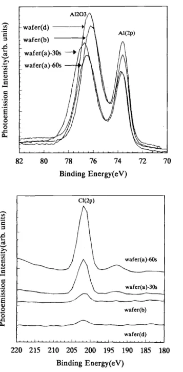
Figure 3a-c shows the XPS spectra of Al (2p), 0 (is), and Cl (2p) for aluminum with different precleanings, respec-tively. It is found that the sample treated with 60 s of vapor phase precleaning [i.e., wafer (a)-60 s] exhibits the highest intensity of Cl as well as the lowest intensities of 0 and A1203 peaks. The result indicates that the HC1 vapor-exposed Al surface was free of oxide and covered with a large amount of Cl species. In addition, the trivial oxygen on wafer (a)-60 s is speculated to be from the reoxidation process during wafer transport under atmospheric ambi-ent before loading into the XPS analyzer. Meanwhile, the (a)-30 s sample gave similar results except it displayed insufficient cleaning (i.e., higher intensity of oxygen signal than that of wafer (a)-60 s). For the (b) group, the quanti-ties of Al-OH bonds were formed on the aluminum surface through the hydrolysis of H20 during the DI water rinsing step. These Al-OH bonds then condense into AlO, and thus a thin oxide rapidly regrows on the aluminum. It causes the high 0 (is) and low Cl (2p) intensities on the
0
1:10 1:5 1:1 2:1 3:1 5:1 10:1
Volume ratio of 35%HC1 to H20 Fig. 2. The removal rates of aluminum exposed under the vapor of HCI solution with various concentrations.
Pump 15 10 5 E E E 0 4) I-, E V
7
/
'U
'I) Ce Ce I-Ce 'I) Ce Ce Ce
0
E V 0 C -Ce l) Ce Ce Ce Ce V Ce -4 Ce C E V0
0
220 215 210 205 200 195 190 185 180
Ce Ce Ce Ce V Ce Ce0
E V C CFig. 3. The XPS spectra of (a, top left) Al (2p), (b, above) 0 (is), and (c, bottom left) Cl (2p) for four types of Al samples with
differ-ent precleaning technologies. The wafer (a)-60 $ and wafer (a)-30 $
are the aluminum samples treated with 60 and 30 s of HCI vapor
precleaning. The (b) samples were treated with aqueous HCI solu-tion, and the (d) samples had no precleaning.
Binding Energy(eV)
aluminum surface (as shown in Fig. 3b and c) even after
precleaning with aqueous HC1 solution.
The selective CVD-W films on submicron trenches and via holes down to aluminum with various precleanings were also investigated, and the results are summarized in Table I. The measured deposition rates are the thickness of tungsten films directly deposited on the unpatterned
alu-minum substrate with 60 s of deposition time, however; not the thickness within trenches and via holes. Figure 4
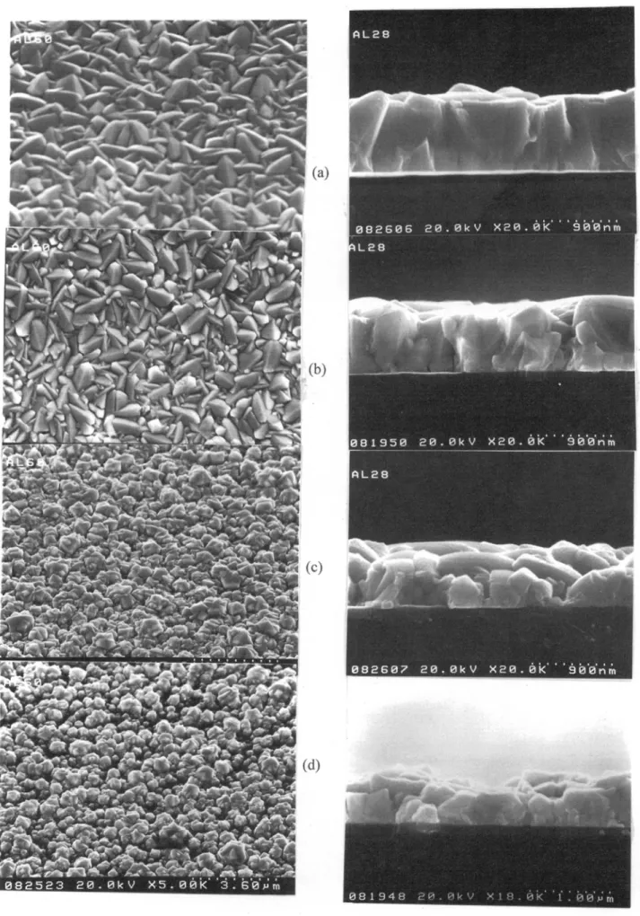
demonstrates the grain structures of CVD-W films
deposited on aluminum with different precleanings. The samples treated with vapor phase precleaning (Fig. 4a and b) have higher deposition rates, denser structures, lower resistivity (13 pit cm), and smoother morphologies than Table I. Selective CVD-W on submicron trenches and via holes with various precleanings.Grain structure and film morphology Deposition rate (nm/mm) Via hole fills
Trench fills Selectivity loss SIMS depth profiles of CVD-W/Al structure X-ray diffraction patterns
450 Fig.6a Fig. 7a Fig. 7a <50 pcs/cm2 Fig. 8a Fig. 9a 356 Fig. 6b >200pcs/cm2 Fig. 8b Fig. 10 Fig. lb Fig. 'lb High selectivity loss
Fig. 8c Fig. 9b 243 Nodeposition No deposition Blanket deposition (No deposition in via hole)
82 80 78 76 74 72 70
Binding Energy(eV)
540 535 530 525
Binding Energy(eV)
520
Wafer group (a)
HCI vapor precleaning Wafer group (b) Aqueous HC1 solution dip
Wafer group (c) In.situSF6/BC13 plasma
precleaning Without any precleaningWafer group (d) 30 s 60 s 120 s
Fig. 4b Fig. 4a Fig. 5 Fig. 4c Fig. 4d
Fig. 4. The SEM micrographs of CVD-W filmson aluminum with different precleanings. Figures (a) and (b) show the aluminum samples
treated with 60 and 30 s of HCI vapor precleaning, respectively, (c) shows the (b) wafers, and (d) the (d) wafers. The selective CVD-W depo-sition parameters are 20 mTorr pressure and 350°C substrate temperature. The flow rates of WF6 and SiH4 are 20 and 12.5 sccm, and the
deposition time is 120s.
wafers (b) and (d) represent similar characteristics, as exhibited in Fig. 4c and d. The as-deposited CVD-W films gave porous, equiaxed, and island-like surface morpholo-gy, which was due to the unremoved aluminum surface oxide that inhibited the nucleation of W Nevertheless, an overlong vapor phase precleaning would induce the coag-ulation of moisture in vapor on the wafer surface. The Al-Cl species on aluminum were hydrolyzed to Al-OH bonds by the excess moisture. While these Al-OH species con-densed into AlO, the aluminum surface was reoxidized again. Figure 5 reveals the SEM micrograph for the CVD-W deposited on Al with 120 s of vapor phase precleaning. Obviously, the right side of picture has the elongate and dense W grains. On the contrary, the left side of picture where the moisture condenses on the wafer, shows the equiaxed island-like W grains and is even without
deposi-tion. This phenomenon was caused by a thin oxide
regrown on the aluminum after an overlong vapor phase precleaning.When the devices are scaled down for ULSI circuit applications, many problems take place in wet cleaning technology. The via holes with small size and high aspect ratios will encounter the issues of cleaning such as wet-ting, surface tension, and bubble formation. As shown in Fig. 6, the (a) group of wafers shows excellent deposition
and fine grain structures for 0.6 p.m size via fills as
opposed to the (b) wafers. The belly-shaped via is caused by the different etching rates between SOG and PECVD oxides during the via etching. The faulty deposition of tungsten in the (b) group is because the precleaning was blocked by wetting, and surface tension issues and the removal of aluminum native oxide was then uncompleted. Except for wet precleaning, other precleaning tech-niques using plasma sputtering'2-'4 or reactive ion etching have been extensively studied. Nevertheless, the etching products (aluminum-containing complexes) formed in the cleaning step could be redeposited on the sidewalls of the trenches and via holes and on the surface of the PECVDoxide. When the reactants (i.e., WF6 and SiH4) of CVD-W
were introduced, the WF6 could react with these products to form W. Simultaneously, the SiH4 adsorbed on etching products would dissociate into Si atoms and then react with WF6 to nucleate W. Both reactions result in the
creep-up and selectivity loss during selective deposition of tung-sten. Figure 7 reveals the SEM micrographs of selective CVD-W for trench and via fills. It is noted that the (c) wafers show an obvious creep-up, failed via fills, and selectivity loss. By contrast, the (a) group possessed
supe-nor deposition and selectivity. Figure 8 demonstrates the selectivity of selective CVD-W for via fills with various precleanings. The selectivity loss defines the number of tungsten particles which deposit on the PECVD oxide per cm2, and we used a dark field optical microscope to count the particles. For the sake of accuracy, we averaged the values of five positions (right, left, center, top, and bottom) on the whole wafer. Every position is 1 cm2 in area. The
statistical values are listed in Table I. The (a) group
(Fig. 8a) shows the completely selective deposition of tungsten, while the (b) group reveals imperfect deposition. In addition, the selectivity of group (b) is inferior to that ofgroup (a). The mechanism of selectivity loss of wafer (b) is
guessed due to the redeposition of the contaminants in the aqueous HC1 solutoin and DI water during precleaning. These contaminants could act as the nucleation sites for W deposition in the sequential CVD-W process. For the case of wafer group (c) with in situ plasma precleaning, a grave
selectivity loss was observed in Fig. 8c. (The detailed cause
was clarified in the above-mentioned discussion.) At the same time, the (d) group (i.e., the sample without any pre-cleaning) showed a blanket deposition of tungsten on the PECVD oxide and no deposition of W inside the via holes. Furthermore, one inherent problem with the CVD-W process for via filling application is the aluminum tnifluo-rides formed by the initial aluminum reduction with WF6 that act as an insulating layer at the CVD-W/Al interface and then greatly degrade the contact properties between
CVD-W and aluminum. Previous have used an additional glue layer (e.g., TiN) on aluminum as a barrier layer to halt the direct reaction between Al and WF6. In Fig. 6. The SEM micrographs for via fills: (a, top) the (a) group of wafers and (b, bottom) the (b) group. Deposition parameters are the same as Fig. 4.
Fig. 5. SEM micrograph of CVD-W film on Al for the sample pre-cleaned with 120s of HCI vapor. The deposition parameters are the same as Fig. 4.
addition, elevating the deposition temperature'8 has also proven to enhance the desorption of A1F3 from the
alu-minum surface through formation of volatile A1F2.
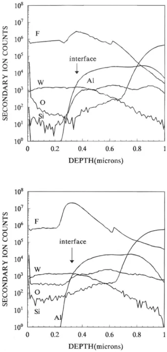
However, the additional glue layer complicates the process and increases the cost, and the high deposition tempera-ture is not compatible with the presence of the underlying aluminum layer.In this study, we have also found that the vapor phase precleaning could reduce the aluminum fluorides pileup at the CVD-W/Al interface. Figure 9a and b illustrates the SIMS depth profiles of CVD-W/Al structures with differ-ent precleanings prior to tungsten deposition. The F con-centration of the (a) group is one order lower than that of the (c) group. At the same time, the impurities of Si and 0 in the tungsten films of (a) are also lower than those of (c). It is conjectured that the Cl species cover the aluminum after HC1 vapor precleaning and occupy the surface active sites to prevent further adsorption of WF6 on Al. The suc-ceeding SiH4 reduction could take place immediately to form a W seed layer, because the negative free energy of
SiH4 reduction was close to that of Al reduction.
Accordingly, the probability of a direct reaction between the WF6 and the underlying Al was suppressed. However, the HC1 vapor phase precleaning cannot completely elim-inate the fluoride pileup at the W/Al interface. Some Cl species were evaporated during the heating step in the deposition process and were replaced by F species when WF6 was dissociated on the aluminum surface. A slightly
high concentration of F was thus observed at the CVD-W/Al interface, as indicated in Fig. 9a.
We have examined the x-ray diffraction patterns for the CVD-W (500 nm) films deposited on the unpatterned alu-minum treated with various precleanings. As shown in
Fig. 10, the (a) group possesses the strongest peak (110) a-W peak without 3-phase tungsten detected. However, the
wafers in group (b) and (c) reveal obvious peaks that cor-respond to the metastable 3-W phase. It is known that the
13-Wlattice is stabilized by impurities like fluorine,29
oxy-gen,3 and silicon.30 These impurities are either from the adequate precleaning procedure prior to CVD-W deposi-tion or are affected by the growth condideposi-tions. In our case of keeping the same deposition parameters through whole experiments, the precleaning should be the dominant fac-tor that determines the crystalline phase of as-deposited tungsten films. Therefore, the 3-W peaks in groups (b) and (c) were conceivably induced by the discrepancy of
pre-cleaning effectiveness.
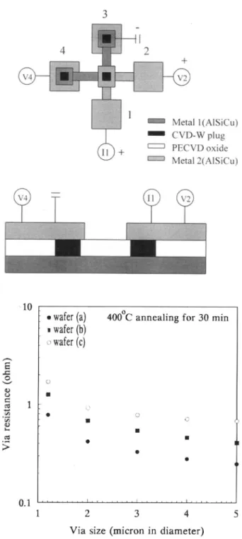
Finally, the electrical characteristics of via resistance were measured using a four-terminal Kelvin structure of an A1SiCu/W/AlSiCu device. The top view and cross-sec-tional diagrams of a four-terminal D-type Kelvin test structure2"2° with W-plugs are shown in Fig. ha. For via resistance measurement, current I3 was forced through pads 1 and 3, and the via resistance R was determined by
sensing the voltage drop V24 between pads 2 and 4 through the relation R = V24/I,3. Figure 1 lb illustrates the
meas-Fig. 7. SEM micrographs for french and via fills: (a, top row) the (a) group of wafers and (b, boitom row) for the (c) group. The deposition parameters are 20 mlorr pressure and 350°C subsfrate temperature. The flow rates of WF6 and SiH4 are 20 and 12.5 sccm, respectively, and the deposition time is 100 s.
Fig. 8. The selectivity loss of selective CVD-W for via fills with var-ious precleanings: (a, top)forthe (a) group, (b, middle) for the (b)
group, and (c, bottom) for the (c) group. Deposition parameters are the same as Fig. 7.
uredvia resistance vs. via size for samples with different precleanings prior to CVD-W. We have known that the via resistance of the W-plug device was affected by the clean-ness of the CVD-W/A1 interface as well as by the resistiv-ity of the W-plug itself. Clearly, the (a) wafers exhibit lower via resistance than the other samples. This is attrib-uted to the reoxidation of the aluminum surface of the group (b) wafers during the DI water rinse step of pre-cleaning. Similarly, the (c) wafers suffer a larger amount of A1F3 formed at the CVD-W/A1 interface, resulting in high
via resistance.
101
100
DEPTH(microns)
Fig.9. The SIMS depth profiles of CVD-W/Al sfructures with
dif-ferent precleaning techniques prior to tungsten deposition: (a, top)
the (a) group, and (b, bottom) the (c) group of wafers.
Summary
A simple and efficient precleaning using hydrochloric
acid vapor prior to selective deposition of tungsten on Al has been shown to remove Al native oxide and to suppress the aluminum fluorides formed at CVD-W/Al interfaces. A large amount of Cl species were detected on the aluminum surface after HC1 vapor precleaning, and the removal rate of aluminum was related to the concentration of reactants used. Moreover, vapor phase precleaning can solve the problems of wetting and bubble formation that occur dur-ing wet precleandur-ing for filldur-ing vias with small size and high aspect ratio. It can also eliminate creep-up and selec-tivity loss induced by precleaning using in situ plasma sputtering or RIE. Our results show a high deposition rate and dense and smooth CVD-W films with low resistivity and low concentration of F formed at the CVD-W/Al interface, resulting in low via resistance.
020627 20.0kV X4.0K
W.Fww WW W W W W
....
•..
. . , . Qt• e e.* . è.s.
•
.
? f' •••
S1533
2a.k')
X4.èk4'g''
108 106iø
iø
i03 102 10' .100 108 i07 106 iosiO
i03 102z
C U7
Cz
C U Cl)z
C Uz
C>
z
0
U Cl) 0 0.2 0.4 0.6 0.8 1 DEPTH(microns) 0 0.2 0.4 0.6 0.8 12 theta
Fig. 10. The XRD patterns of selective CVD-W (500 nm) films deposited on the unpcitterned aluminum treated with various
pre-cleanings: (1) a-W(1 10), (2) Al(1 11), (3) a-W(200), (4)a-W(21 1), and (5) 13-W(321).
Acknowledgments
This work is supported by National Science Council, Taiwan, under Grant No. NBC 85-2215-E-009-061.
Manuscript submitted Jan. 16, 1996; revised manuscript
received Oct. 14, 1996.
National Chiao Tung University assisted in meeting the publication costs of this article.
REFERENCES
1. J. E. J. Schmitz, Chemical Vapor Deposition of Tung-sten and TungTung-sten Suicides for VLSI/ULSI Appli-cation, Chap. 1, Noyes Publications, Park Ridge, NJ
(1991).
2. E. K. Broadbent and C. L. Ramiller, This Journal, 131,
1427(1984).
3. H. H. Busta and C. H. Tang, ibid., 133, 1195 (1986). 4. M. Wong, N. Kobayashi, R. Browning, D. Paine, and K.
C. Sarawat, ibid., 134, 2339 (1987).
5. M. L. Yu, K. Y. Ahn, and R. V. Joshi, J. Appl. Phys., 67, 1055 (1990).
6. M. L. Yu and B. N. Eldrige, J. Vac. Sci. Technol., A7,
626 (1989).
7. T. Tsutsumi, H. Kotani, J. Komori, and S. Nagao, IEEE Trans. Electron. Devices, ED-37, 569 (1990). 8. J. M. DeBlasi, D. K. Sadana, and M. H. Norcott, Mater.
Res. Symp. Proc., 71, 303 (1986).
9. E. K. Broadbent and W. T. Stacy, Solid-State Technol.,
28, 51 (1985).
10. E. K. Broadbent, J. Vac. Sci. Technol., B5, 1661 (1987).
11. V. V. S. Rana, J. A. Taylor, L. H. Holschwandnei and N. S. Tsai, in Tungsten and Other Refractory Metals for VLSI Applications III, Victor A. Wells, Editor,
p. 187, MRS, Philadelphia, PA (1987).
12. R. C. Ellwanger, J. E. J. Schmitz, and A. J. M. Van Dijk, ibid., p. 399.
13. E. Nishitani and S. Tsuzuku, in Tungsten and Other Advanced Metals for VLSI! ULSI Applications 1 S. S. Wong and S. Furukawa, Editors, p. 61, MRS, Philadelphia, PA (1989).
14. S. L. Ng, S. J. Rosner, D. R. Bradbury, T. I. Kamins, and
S. S. Laderman, in Tungsten and Other Refractory Metals for VLSI Applications II, E. K. Broadbent,
Editor, p. 93, MRS, Philadelphia, PA (1986). 15. D. R. Bradbury, J. E. Turner, K. Nauka, and K. Y. Chiu,
IEDM Proc., 273 (1991).
16. M. L. Yu, K. Y. Ahn, and R. V. Joshi, in Tungsten and Other Refractory Metals for VLSI Applications II, E. K. Broadbent, Editor, p. 93, MRS, Philadelphia,
PA (1986).
1 2 3 4 5
Via size (micron in diameter)
Fig. 11. (a, top) lop view and cross-sectional diagrams of a
D-type four-terminal Kelvin test structure for measuring via resistance
of the AISiCu/W/AlSiCu device. (b, bottom) Via resistance vs. via
size for three samples with different precleanings.
17. M. L. Yu, K. Y. Ahn, and R. V. Joshi, IBM J. Res. Develop., 34, 875 (1990).
18. D. Alugbin, D. Favreau, D. Kostelnick, K. Olasupo, and J. Shimer, in Tungsten and Other Refractory Metals for VLSI Applications II, E. K. Broadbent,
Editor, p. 93, MRS, Philadelphia, PA (1986).
19. P. E. Riely, S. S. Peng, and L. Fang, Solid-State
Tech-nol., 36, 47 (1993).
20. P J. Holmes and J. E. Snell, Microelectron. Reliab., 5,
377 (1966).
21. R. E. Novak, Solid-State Technol., 31, 41 (March 1988). 22. B. E. Deal, M. A. McNerlly, D. B. Kao, and J. M.
deLarios, ibid., 33, 73 (July 1990).
23. C. R. Cleavelin and G. T. Duranko, Semicond. Int., 94
(Nov. 1987).
24. B. E. Deal and C. R. Helms, Handbook of
Semicon-4)
Jwafer(c)afer(c)
wafer(b) wafer(a)AA
30 40 50 60 70 80 Metal I(AIS1Cu) CVD-W plug PECVD oxide Metal 2(AISiCu) 10 E 0 V C) Cd rd 4) I-Cd>
• wafer (a) 400°C annealing for 30 mm • wafer (b) wafer(c) L a
•
U.
•
•
1 0. 1p.280, Noyes Publications, Park Ridge, NJ (1993). 25. N. Miki, H. Kikuyama, I. Kawanabe, M. Miyashita,
and T. Ohmi, IEEE Trans. Electron Devices, ED-37, 107(1990).
26. N. Miki, H. Kikuyama, M. Maeno, J. Murota, and T.
Ohmi, IEDM Proc., 730 (1988).
27. W. M. Loh, S. E. Swirhun, T. A. Schreyer, R. M.
Swan-son, and K. C. Saraswat, IEEE Trans. Electron
De-28. J. Santander, M. Lozano, and C. Cane, ibid., ED-40,
944(1993).
29. C. C. Tang and D. W. Hess, Appl. Phys. Lett., 45,633
(1984).
30. J. E. J. Schmitz, M. J. Buiting, and R. C. Ellwanger, in Tungsten and Other Refractory Metals for VLSI Ap-plications IV R. S. Blewer and C. M. McConica, Editors, p. 27 (1988).
Thermal Oxidation of Tungsten-Based Sputtered Coatings
C. Louro and A. CavaleiroDepartamento de Engenharia Mecânica-Polo II, Pinhal de Marrocos, 3030 Coimbra, Portugal
ABSTRACT
The effect of the addition of nickel, titanium, and nitrogen on the air oxidation behavior of W-based sputtered coat-ings in the temperature range 600 to 800°C was studied. In some cases these additions significantly improved the oxida-tion resistance of the tungsten coatings. As reported for bulk tungsten, all the coatings studied were oxidized by layers following a parabolic law. Besides W03 and WOr phases detected in all the oxidized coatings, Ti02 and NiWO4 were also detected for W-Ti and W-Ni films, respectively. WO was present as an inner protective compact layer covered by the porous W03 oxide. The best oxidation resistance was found for W-Ti and W-N-Ni coatings which also presented the high-est activation energies (E =234and 218 kJ mol, respectively, as opposed to E 188 kJ mol' for the other coatings). These lower oxidation weight gains were attributed to the greater difficulty of the inward diffusion of oxygen ions for W-Ti films, owing to the formation of fine particles of W-Ti02, and the formation of the external, more protective layer of
N1WO4 for W-N-Ni coatings.
Introduction
Muchresearch work has been carried out in the last few decades on the development of hard coatings for mechan-ical applications. Besides very high hardness and adhe-sion, these coatings should be thermally stable and oxida-tion resistant in order not to fail when service temperatures
reach several hundred degrees Celsius. For example, during
cutting operations temperatures as high as 900°C can be reached at the tip of the tool.
Hard coatings of the system W-N/C-M (M=Ti, Ni) have been developed as an alternative to titanium-based coat-ings, which are extensively used in industrial applications. In spite of the very high hardness (in some cases over 45 GPa) and high scratch-test adhesion (critical loads of over 60 N when the coating is deposited on high-speed steel), some of these coatings do not exhibit corresponding excel-lent behavior in their applications, particularly in cutting operations. The influence of interstitials and of the M ele-ments (as defined) on the mechanical properties of tung-sten-based coatings is known; however, in order to under-stand the cutting performance of these coatings, more knowledge is needed about the influence of these elements on oxidation resistance at high temperatures.
In the development of high-temperature bulk materials,
it was observed that oxidation resistance could be
improved by the addition of "active elements." Many sug-gestions have been put forward to explain the effects of these elements. For example, it has been suggested that active elements can act as preferential nucleation sites in the oxidation process, leading to the formation of a pro-tective scale; that active elements can form an intermedi-ate inner oxide layer which acts as a diffusion barrier or as a mechanical buffer; that active elements can reduce the accumulation of voids at the oxide-alloy interface; and that active elements can modify the oxide morphology.'3The modification of the oxide microstructure and the presence of active elements, either in solid solution, segre-gated, or as precipitates in the oxide scale, can have an influence on the diffusion rates and the mechanical prop-erties of the oxide scales, playing an important role in the oxidation behavior of the materials.
The beneficial influence of certain reactive elements, such as Al and Cr, on oxidation behavior at high tempera-tures is a well-known phenomenon,"4 but very little is known about the influence of other reactive elements, such as Ti and Ni. Moreover, in spite of the large amount of research work carried out on the high-temperature oxi-dation behavior of tungsten and tungsten-based alloys, very little is known about its behavior in the form of thin coatings.
In a previous paper5 we presented the influence of Ti and
Ni on the thermal behavior of sputtered W-N coatings in the temperature range 600 to 800°C. It was found that W-N-Ni films presented a much higher oxidation resistance than single W-N and W-Ti-N films. In this paper we pre-sent the results of a more global investigation comprising our previous study and extended to sputtered W coatings deposited from single or compound targets (with Ni and Ti) in a nonreactive atmosphere.
Experimental
Deposition
The films were deposited by dc reactive magnetron sput-tering with a specific target power density of 10 W cm2 and a negative substrate bias of 70 V. Targets were W, W-10%Ti, and W-10%Ni (mass fractions). When the reactive mode was used the N2/Ar partial pressure ratio was 1/2, for a total deposition pressure of 3 x 10 Pa. The sub-strates (5 x 5 X 1 mm) of steel (Wi -AISI)were polished down to a diamond paste of 1 p.m. To completely coat the entire surface, the substrates were glued with precision in one of its lateral faces. Owing to the rotational movement of the substrate holder, all the faces were uniformly coat-ed. Before deposition, the sputtering chamber was evacu-ated by a turbomolecular pump down to a final pressure of ltY4 Pa. The substrate surfaces were then ion cleaned by an ion gun. The cleaning procedure included a first elec-tron heating up to temperatures close to 450°C and after-ward, Ar bombardment for 8 mm (ion gun settings at 20 A, 40 \1 substrates at —120 V). The deposition time was selected such that a final thickness in the range 3 to 4 p.m