Novel Isolated High-step-up DC-DC Converter with Voltage Lift
10
0
0
全文
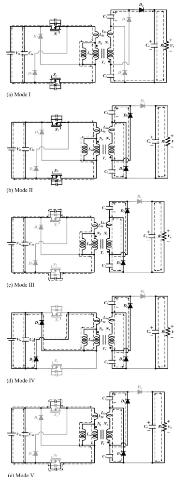
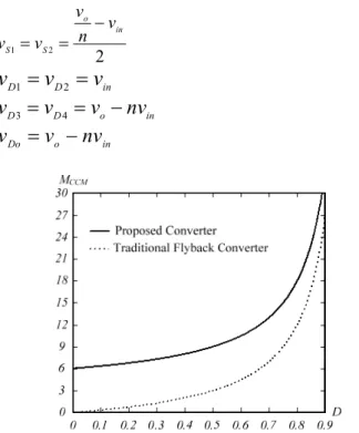
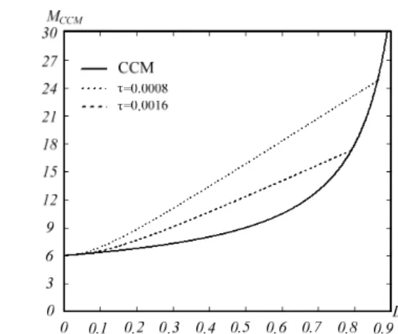
(2)
(3)
(4)
(5)
(6)
(7)
(8)
(9)
數據


+3
相關文件
Now, nearly all of the current flows through wire S since it has a much lower resistance than the light bulb. The light bulb does not glow because the current flowing through it
According to the Heisenberg uncertainty principle, if the observed region has size L, an estimate of an individual Fourier mode with wavevector q will be a weighted average of
Holographic dual to a chiral 2D CFT, with the same left central charge as in warped AdS/CFT, and non-vanishing left- and right-moving temperatures.. Provide another novel support to
* Anomaly is intrinsically QUANTUM effect Chiral anomaly is a fundamental aspect of QFT with chiral fermions.
In this paper, motivated by Chares’s thesis (Cones and interior-point algorithms for structured convex optimization involving powers and exponentials, 2009), we consider
Developmentally Appropriate Practice in Early Childhood Programs.. Washington, DC: National Association for the Education of
Developmentally Appropriate Practice in Early Childhood Programs.. Washington, DC: National Association for the Education of
Developmentally Appropriate Practice in Early Childhood Programs.. Washington, DC: National Association for the Education of
