Analysis and Design of a Novel Single-phase Full-bridge Soft-switching Rectifier
Maoh-Chin Jiang, Shyh-Shing Perng, Chien-Ming Wang, Ter-Feng Wu, Ching-Hsien Ke, and Jing-Jhu Jhan Department of Electrical Engineering
National Ilan University Yilan, Taiwan, R.O.C.
Abstract—A novel single-phase full-bridge soft switching rectifier (FBSSR) using a new resonance unit is proposed in this paper. All main switches in the proposed soft switching rectifier operate at zero-voltage-switching (ZVS) turn-on and turn-off.
Moreover, the auxiliary switches operate at zero-current- switching (ZCS) turn-on and turn-off. Major benefits of this novel rectifier are found in efficiency improvement, and reduced dv/dt. Besides, the proposed rectifier achieves a unity power factor, a sinusoidal input current and a bidirectional power flow capability. A small-signal model is derived and, in addition to the feedback control, an adaptive feed-forward controller is proposed to achieve almost zero output impedance and zero audio susceptibility. Finally, a prototype hardware circuit is constructed, and some experimental results are presented for demonstration.
Keywords-full bridge soft-switching rectifier, zero-voltage- switching (ZVS), zero-current-switching (ZCS)
I. I
NTRODUCTIONThe pulse-width-modulated (PWM) rectifier is used increasingly in a wide diversity of applications: power supplies for microelectronics, electronic ballasts, dc motor drives, battery charging, and power conversion. The topology usually employs power factor correction single-phase power supplies composed of a front end rectifier followed by a boost converter [1]-[2]. Due to the switching losses and the limitations of semiconductor devices that are currently available, the switching frequency of hard-switching PWM converters is usually around a few kilohertz. Although, power density and transient response are improved with higher switching frequencies, the high frequency power conversion causes problems such as increase of switching stresses on the power devices, increase of switching losses, and generation of electromagnetic interference (EMI) due to a high dv/dt for high frequency switching operation. To improve the performance of the PWM rectifier, various single-phase soft- switching rectifiers using either zero-voltage switching (ZVS) or zero-current switching (ZCS) have been proposed in the literature [3]-[5]. The basic issue has always achieved high frequency operation with reduced switching losses and EMI.
However, most of single-phase soft-switching rectifiers are suited for applications where power is transmitted only from the ac source to the dc load [3]-[7]. There are several applications where energy flow can be reversed during the
Lr
C 3
vcr
4
vcr 1
vcr
2
vcr vac
Ls
S1 S3
S4 S2
S6
ro
is
+
− vo
1
Vgs
vtri
is
vo
*
vo ac ac
v v
*
is ) (switching
S
) (switching
S
off on
on off
on off
2:
1S S
4:
3S S
5: S
6: S
on
off on
off S5
io
io
*
vo
vs
+ +
2
Vgs Vgs3 Vgs4 Vgs5 Vgs6
Iff
Itb
A B
D1
D4
D3
D2
Fig. 1. The block diagram of the proposed soft-switching rectifier.
operation, such as with locomotives, downhill conveyers, etc.
In all these applications, the line-side converter must be able to deliver energy back to the power supply [6]-[8]. A novel single-phase full-bridge soft-switching rectifier with a bidirectional power flow capability is proposed in this paper.
All main switches operate at zero-voltage-switching (ZVS) turn-on and turn-off. Furthermore, the auxiliary switches operate at zero-current-switching (ZCS) turn-on and turn-off.
Major benefits of this novel rectifier are found in efficiency
improvement, and reduced dv/dt. Besides, the proposed
rectifier achieves a unity power factor, sinusoidal input current
and a bidirectional power flow capability. In addition to the
feedback, a simple feed-forward compensator is proposed to
achieve almost zero output impedance and zero audio
susceptibility characteristics.
II. P
ROPOSEDS
OFT-S
WITCHINGR
ECTIFIERA. Full-bridge Soft-Switching Rectifier
A block diagram of the proposed FBSSR is shown in Fig.
1. It consists mainly of a power stage, a voltage controller, a feed-forward controller, a current reference generator, a current controller, a PWM switching scheme, and a zero voltage switching signal generator. The power stage can be divided into two sections. The first section is a conventional full-bridge PWM rectifier. It is composed of switches S
1, S
2, S
3, and S
4, their body diodes D
1, D
2, D
3, and D
4, an input boost inductor L
Sand an output capacitor C. The second section is the proposed new simple ZVS-PWM commutation cell, composed of S
5, S
6, L
r, C
r1, C
r2, C
r3, and C
r4. This section is synchronous with the circuit of the first section. It provides the ZVS on all semiconductors in the full-bridge PWM rectifier.
B. Principle of Operation
To simplify the analysis, the following assumptions are made during one switching cycle: (i) input boost inductor L
Sis sufficiently large that the input current can be considered to be ripple-free, i
S=I
S; (ii) the output capacitor C is large enough that the dc output voltage can be assumed to be constant, v
o=V
dc; (iii) all values of resonant capacitors are identical, i.e., C
r1=C
r2=C
r3=C
r4≡C
r, where C
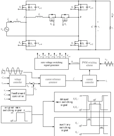
ris the sum of the MOSFET’s parasitic capacitance; and (v) all components and devices are ideal. On the basis of these assumptions, the circuit operations in one switching cycle can be divided into eight modes. The eight dynamic equivalent circuits are shown in Fig. 2. The theoretical waveforms of the proposed soft-switching rectifier are shown in Fig. 3.
Mode 0 (t < t0): Initially, assume that the switches S1
and S
2are conducting the source current, and that the initial conditions are the resonant voltages v
cr1(t)=v
cr2(t)=0 and the resonant voltages v
cr3(t)=v
cr4(t)=V
dc. The auxiliary switches S
5and S
6are turned off and the resonant current i
Lr(t)=0, as shown in Fig. 2(a). The resonant current and capacitor voltages can be described as
0 ) ( t =
i
Lr(1)
0 ) ( )
(
21
t = v t =
v
cr cr(2)
dc cr
cr
t v t V
v
3( ) =
4( ) = (3)
Mode 1 (t0
< t < t
1): As shown in Fig. 2(b), this modebegins when S
5is turned on with ZCS at t = t
0. The resonant inductor L
rcharges linearly from output dc voltage V
dc. The resonant current i
Lr(t) is increased linearly. This mode ends when the switches S
1and S
2are turned off with ZVS at t=t
1. The resonant current and capacitor voltages can be described as
) ( )
( t t
0L t V i
r dc
Lr
= − (4)
0 ) ( )
(
21
t = v t =
v
cr cr(5)
dc cr
cr
t v t V
v
3( ) =
4( ) = (6)
Mode 2 (t1
< t < t
2): As shown in Fig. 2(c), the resonantinductor L
rand the resonant capacitors C
r1, C
r2, C
r3and C
r4form a resonant tank. At first, the resonant current i
Lr(t) increases and then decreases when it reaches its peak value.
This mode is finished when the resonant voltages v
cr3(t) and v
cr4(t) drop to zero and the resonant voltages v
cr1(t) and v
cr2(t) reach V
dc. The resonant current and capacitor voltages can be described as
[
1 cos ( )]
) ( sin ) ( cos ) ( )
( 1 1 t t1 I t t1
Z t V t t
i t
i r s r
o r dc
L
Lr = r
ω
− +ω
− + −ω
−(7)
[ 1 cos ( ) ]
) 2 ( )
(
2 11
V t t
t v t
v
cr=
cr=
dc− ω
r−
[ ( ) ] sin ( )
2 i t
1I t t
1Z
r s L o
r
− −
+ ω (8)
[ 1 cos ( ) ]
) 2 ( )
(
4 13
V t t
t v t
v
cr=
cr=
dc+ ω
r−
[ ( ) ] sin ( )
2 i t
1I t t
1Z
r s L o
r
− −
− ω (9)
where
r r
r
L C
= 1
ω (10)
r o r
C
Z = L (11)
denote the natural frequency and characteristic impedance of the resonant circuit, respectively.
Mode 3 (t2
< t < t
3): As shown in Fig. 2(d), since the resonant voltages v
cr3(t) and v
cr4(t) equal zero, the body diodes D
3and D
4start to conduct. The switches S
3and S
4are turned on during this interval with ZVS commutation. The energy stored in the resonant inductor L
ris delivered back to the output dc voltage. The resonant current i
Lr(t) is decreased linearly. This mode ends when the resonant current i
Lr(t) drops to zero. The resonant current and capacitor voltages can be described as
) ( ) ( )
(
2t t
2L t V i t i
r dc L
Lr
=
r− − (12)
dc cr
cr
t v t V
v
1( ) =
2( ) = (13)
0 ) ( )
(
43
t = v t =
v
cr cr(14)
Mode 4 (t3
< t < t
4): As shown in Fig. 2(e), the switches S
3and S
4are conducting the source current, and the resonant voltages v
cr3(t)=v
cr4(t)=0 and the resonant voltages v
cr1(t)
=v
cr2(t) =V
dc. The auxiliary switches S
5and S
6are turned off
1250
and the resonant current i
Lr(t)=0. The resonant current and capacitor voltages can be described as
0 ) ( t =
i
Lr(15)
dc cr
cr
t v t V
v
1( ) =
2( ) = (16)
0 ) ( )
(
43
t = v t =
v
cr cr(17)
Mode 5 (t4
< t < t
5): As shown in Fig. 2(f), this mode begins when the auxiliary switch S
6is turned on at ZCS at t=t
4. The resonant inductor L
rcharges linearly from output dc voltage V
dc. The resonant current i
Lr(t) is decreased linearly.
This mode ends when the switches S
3and S
4are turned off with ZVS at t=t
5. The resonant current and capacitor voltages can be described as
) ( )
( t t
4L t V i
r dc
Lr
= − − (18)
dc cr
cr
t v t V
v
1( ) =
2( ) = (19)
0 ) ( )
(
43
t = v t =
v
cr cr(20)
Lr
3 vcr
4 vcr
1 vcr
2 vcr
S1 S3
S4 S2
S6
Is Vdc
S5 Lr
A i
B
Lr
3 vcr
4 vcr
1 vcr
2 vcr
S1 S3
S4 S2
S6
Is Vdc
S5 Lr
A i
B
Lr
3 vcr
4 vcr
1 vcr
2 vcr
S1 S3
S4 S2
S6
Is Vdc
S5 Lr
A i
B
Lr
3 vcr
4 vcr
1 vcr
2 vcr
S1 S3
S4 S2
S6
Is Vdc
S5 Lr
A i
B
Lr
3 vcr
4 vcr
1 vcr
2 vcr
S1 S3
S4 S2
S6
Is Vdc
S5 Lr
A i
B
Lr
3 vcr
4 vcr
1 vcr
2 vcr
S1 S3
S4 S2
S6
Is Vdc
S5 Lr
A i
B
Lr
3 vcr
4 vcr
1 vcr
2 vcr
S1 S3
S4 S2
S6
Is Vdc
S5 Lr
A i
B
Lr
3 vcr
4 vcr
1 vcr
2 vcr
S1 S3
S4 S2
S6
Is Vdc
S5 Lr
A i
B
Fig. 2. Operation modes of the proposed soft-switching rectifier.
Mode 6 (t5
< t < t
6): As shown in Fig. 2(g), the resonant inductor L
rresonates with the resonant capacitors C
r1, C
r2, C
r3and C
r4again. At first, the resonant current i
Lr(t) decreases and then increases when it reaches its negative peak value. The resonant voltages v
cr1(t) and v
cr2(t) are decreased. The resonant voltages v
cr3(t) and v
cr4(t) are increased. This mode ends when the resonant voltages v
cr3(t) and v
cr4(t) reach V
dcand the resonant voltages v
cr1(t) and v
cr2(t) drop to zero. The resonant current and capacitor voltages can be described as
[
1 cos ( )]
) ( sin ) ( cos ) ( )
( 5 5 t t5 I t t5
Z t V t t
i t
i r s r
o dc r
L
Lr =− r ω − − ω − + − ω −
(21)
[ 1 cos ( ) ]
) 2 ( )
(
2 51
V t t
t v t
v
cr=
cr=
dc+ ω
r−
[ ( ) ] sin ( )
2 i t
5I t t
5Z
r s o L
r
+ −
− ω (22)
[ 1 cos ( ) ]
) 2 ( )
(
4 53
V t t
t v t
v
cr=
cr=
dc− ω
r−
[ ( ) ] sin ( )
2 i t
5I t t
5Z
r s L
o
r
+ −
+ ω (23)
2 1, gs
gs V V
5
Vgs
6
Vgs
Lr
i
1 Cr
v
S1
i
2 Cr
v
S2
i
3 Cr
v
S3
i
4 Cr
v
S4
i
vAB
t0t1t2t3 t4t5t6t7 Ts
D) 1 ( −
Ts
t8
t
t
t
t
t
t t
t t
t
t
t
t
max ,
Is
Vdc
Vdc
−
4 3, gs
gs V
V
max ,
Is
−
t
Fig. 3. Theoretical waveforms of the proposed soft-switching rectifier.
Mode 7 (t6
< t < t
7): As shown in Fig. 2 (h), since the resonant voltages v
cr1(t) and v
cr2(t) equal zero, the body diodes D
1and D
2start to conduct. The switches S
1and S
2are turned on during this interval with ZVS commutation. The energy stored in the resonant inductor L
ris delivered back to the output dc voltage. The resonant current i
Lr(t) is increased linearly. This mode ends when the resonant current i
Lr(t) drops to zero. The resonant inductor current and capacitor voltages can be described as
) ( )
( )
(
6t t
6L t V i t i
r dc Lr
Lr
= + − (24)
0 ) ( )
(
21
t = v t =
v
cr cr(25)
dc cr
cr
t v t V
v
3( ) =
4( ) = (26)
After mode 7, the circuit operation is returned to mode 0.
Through the analysis presented above, key waveforms of the proposed FBSSR can be plotted as shown in Fig. 3.
III. D
ERIVATION OF THED
YNAMICM
ODELFor convenient controller design, a dynamic model of the rectifier is derived in this section. It is assumed that the parasitic loss can be neglected and the input current is sinusoidal and in phase with the voltage source. Hence, from conservation of power, one can obtain
o o
o
r
Cv v dt vi d
2 2
] 2
[ 1 +
= (27)
where v and i are the RMS voltage and current of ac source, respectively. Equation (27) means that the input power is equal to the sum of the increased power stored in the capacitor and the power delivered to the load. The dynamic behavior of the inductor can be neglected because the input current has been controlled by the fast response current controller. The small signals v~ ,
i~, r~ ,
ov~ are defined according to the
ofollowing relations
v V
v = + ~ (28)
i I
i ~
+
= (29)
o o
o
R r
r = + ~ (30)
o o
o
V v
v = + ~ (31)
Then, by using the above small perturbation and after linearization, we obtain the DC equation from (27),
o o
R VI V
2
= (32)
and the small signal state equation
o o
o o
o o o
o o o o
o o o o
CV i i VIR CV v V CV v I CR
V r CR i VI CV v V CV v I CR dt
v d
~
~ ~ 2 ~
~ ~
~ 2 ~
~
−
2+ +
−
≅
+ +
+
−
= (33)
It follows from (33) that the control-to-output transfer function
i vo
T
~,~, the output impedance transfer function
o oi
T
v~,~, and the
line-to-output transfer function T
v~o,v~take the following forms
a s
b
s CR CV
V
i T v
o o v
i o i
vo o ≅ +
+
=
≅ ~ == 2
~
)
~0 (~ ,~
~
(34)
a s
c
s CR CV
VIR
i T v
o o
o i
v o o i
voo +
≅ − +
−
=
≅~ == 2
~ 2
)
~0 (~ ,~
~
(35)
a s
d
s CR CV
I
v T v
o o i
i o v
vo o
≅ + +
=
≅ ~ == 2
~
)
~0 (~ ,~
~
(36)
IV. D
ESIGN OF THEF
EED-
FORWARDC
ONTROLLERTo achieve zero output impedance and zero audio susceptibility, Fig. 4 shows the block diagram of the proposed control strategy. There are three inputs and one output. Also, for simplicity, proportional control is chosen for the feed- forward controller, and a simple PI control is chosen for the feedback controller (G
c(s)). It follows from Fig. 4 that one can obtain
~) ( ) ( ) ( 1
)
~ ( ) ( ) ( 1
)
~ ( ) ( ) ( 1
) )(
~ ( *
o f
c i
f c
v o
f c c
o i
a s K b s G
a s F b a s
c v a s K b s G
a s F b a s
d v a s K b s G
a s s b G
v −
+ +
− + + + + +
− + + + + +
= +
(37) Thus, from (37) one has
) ( ) ( 1
) (
~
~
a s K b s G
a s F b a s
c i Z v
f c
i o
o out
+ +
− +
= +
−
≅
(38)
) ( ) ( 1
) (
~
~
a s K b s G
a s F b a s
d v S v
f c o v v
+ +
− +
= +
≅
(39)
where Z
outis the output impedance and S
vis the audio susceptibility. It is now obvious to see that by choosing
v v b
F
i= c =
o(40)
v
2i v b
F
v= d =
oo(41)
one can achieve simultaneously
Z
out=0 and S
v=0 (42)
In addition, the closed-loop transfer function now becomes
⎟ ⎠
⎜ ⎞
⎝
⎛ + +
⎟ ⎠
⎜ ⎞
⎝
⎛
= +
≅
a s K b s G
a s s b G v
s v T
f c c
o o c
) ( 1
) (
~ ) ~
(
*(43)
Thus, from (43) it can be seen that due to addition of the proposed feed-forward control, the influence of the line voltage variation and the output current variation can now be eliminated. Also, from (40) and (41) it can be seen that F
iand
1252
F
vare independent of all circuit parameters. In fact, it is
Σ Gc(s) Σ s a
b
+ Σ
Fv Fi s a
c + a s
d +
~*
vo
Kf
v~ i~o
v~o
− + +
+ +
−
~i
+ −
itb
~
Fig. 4. The control block diagram of the proposed soft-switching rectifier.
possible to implement a feed-forward controller using these equations as follows. From Fig. 4, we obtain
tb o o o o
tb v o i
i v v
i i v v v
i v F i F i
~ ~ ~
~ ~ ~
~
2
+
−
=
+
−
=
tb
x
i
i ~
~ +
≅ (44)
where
~itbis the output of the feedback controller G
c(s).
Because of variations of the line voltage and the output load, to achieve zero Z
outand zero S
v, values of F
iand F
vshould be adapted as well. It is interesting to note that if we choose i
xand v
oas follows
) (
) )(
(
*v K
v K i i K
v o vo o io
x
≅ (45)
v o vo io
o
K
v K v K
*
≅ (46)
where K
iois the scale factor of the current sensor, K
vois the scale factor of the reference voltage sensor, and K
vis the scale factor of the line-voltage detector, then from (45) the corresponding first-order small-signal equation can be obtained
v v i i i
i i
o xo
x x
~ ~
~
∂ + ∂
∂
= ∂
v v i i v v
v
ooo
~
o~
−
2= (47)
which matches the result in (44).
Therefore, the proposed feed-forward controller can be simply implemented using only one analogue computational unit (AD538) [11].
V. E
XPERIMENTALR
ESULTSTo confirm the feasibility and performance of the proposed soft-switching rectifier, a prototype is constructed with the following parameters.
1) Input voltage: v
ac= 110 V
rms. 2) Output voltage: v
o= 200 V.
3) Input boost inductor: L
s= 1.5 mH.
4) Resonant inductor: L
r= 30 uH.
5) Output capacitor: C = 470 uF.
6) Rated output power: P
o= 400 W.
7) Switching frequency: f
s= 40 kHz.
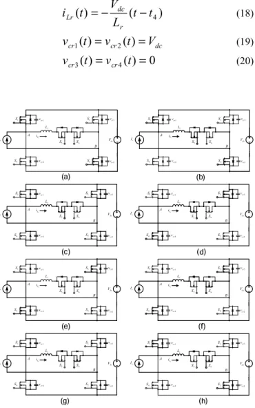
The commutation phenomenon in the main switches S
1, S
2, S
3and S
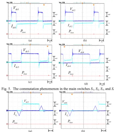
4are measured in Fig. 5 and the commutation phenomenon in the auxiliary switches S
5and S
6are measured in Fig. 6. The experimental results shown in Fig. 5 demonstrate that ZVS is achieved at constant frequency for the switches (S
1, S
2, S
3, S
4). Also, the experimental results shown in Fig. 6 demonstrate that ZCS is achieved at constant frequency for the switches (S
5and S
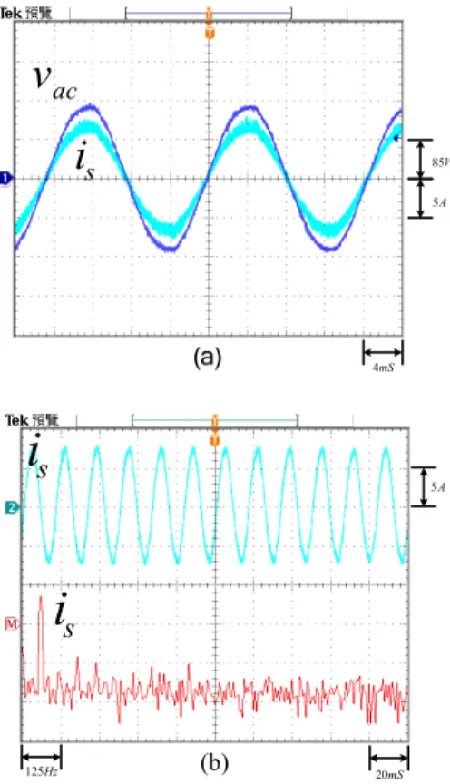
6). Therefore, the switching energy losses for the proposed rectifier are practically zero. Fig. 7(a) shows the experimental waveforms v
acand i
s. The line current is indeed in phase with the input line voltage and with a clear sinusoidal waveform. Fig. 7(b) shows the frequency spectrum of i
s. The total harmonic distortion (THD) of the line current is 2.81% and the power factor is 0.99. Fig. 8 shows the transient responses of line voltage v
ac, line current i
s, output dc voltage v
o, and output dc current i
ounder a step load change from 50W to 400W. From Fig. 8 one can find that the proposed rectifier has good dynamic performance. At rated load, the efficiency gain obtained with the soft-switching rectifier is 2.5% higher than the hard switched counterpart.
V 100
A 5
uS 4
1
Ids 1
Vds
kW 1
V 100
A 5
uS 4 2
Ids 2
Vds
kW 1
V 100
A 5
uS 4
3
Ids 3
Vds
kW 1
Ploss
V 100
A 5
uS 4
4
Ids
4
Vds
kW 1
Ploss
Ploss Ploss
Fig. 5. The commutation phenomenon in the main switches S1, S2, S3, and S4.
V 100
A 5
uS 2
Lr
I
5
Vds
kW loss 1
P
V 100
A 5
uS 2
Lr
I
6
Vds
kW loss 1
P
Fig. 6. The commutation phenomenon in the auxiliary switches S5 and S6.
VI
. C
ONCLUSIONSIn this paper, analysis, design and control of a novel single-phase full-bridge soft-switching rectifier with a unity power factor, a sinusoidal input current, a regulated dc output and a bidirectional power flow capability have been presented.
In the proposed soft-switching rectifier, all main switches operate at ZVS turn-on and turn-off, and the auxiliary switches operate at ZCS turn-on and turn-off. Therefore, the proposed rectifier performs significantly better than its hard- switching counterpart in switching loss and dv/dt reduction.
Moreover, a small signal model is derived and, in addition to the feedback control, an adaptive feed-forward control is proposed to achieve good dynamic regulation. Finally, some experimental results are provided to demonstrate the effectiveness of the proposed soft-switching rectifier.
V 85
mS 4
A 5
v ac
i s
(b) 20mS
A
s
5i
Hz 125
i s
Fig. 7. (a) Waveforms of vac and is. (b) Spectrum of is.
mS 40
A 10
A 2
V 500
V 300
Fig. 8. Waveforms of vac, is, vo and io under a step load change from 50W to 400W.
R
EFERENCES[1] N. Mohan, T. M. Undeland, and W. P. Robbins, “Power electranics : converters, appleications and design,” John Wiley and Sons, 2003.
[2] C. M. Wang, C. H. Su, C. H. Lin, M. Y. Liu, M. C. Jiang, and K. L.
Fang, “A ZVS-PWM voltage-doubler rectifier with high power factor,”
IEEE International Confcrence on Industrial Techonlogy, pp. 1-5, 2008.
[3] A. F. de Souza and I. Barbi, “A new ZVS-PWM unity power factor rectifier with reduced conduction losses,” IEEE Transaction on Power Electronics, vol. 10, pp. 746-752, no. 6, 1995.
[4] X. Yuan and I. Brabi, “Analysis, designing, and experimentation of a transformer-assister PWM zero-voltage-switching pole inverter,” IEEE Transactions on Power Electronics, vol. 15, no. 1, pp. 72-82, 2000.
[5] G. Hua and C. S. Leu and F. C. Lee, “Novel zero-voltage-transition PWM converters,” IEEE Trans. on Industrial Electronics, vol. 42, no. 6, pp. 595-603, 1995.
[6] O. Stihi and B. T. Ooi, “A single-phase controlled-current PWM rectifier,” IEEE Trans. on Power Electronics, vol. 3, no. 4 , pp. 453-459, 1988.
[7] O. Garcia, J. Cobos, R. Prieto, P. Alou, and J. Uceda, “Single phase power factor correction : A surrey,” IEEE Trans. Power Electron., vol.
18, no. 3, pp. 749-755, 2003.
[8] T. Israeli, I. Levin, D. Shmilovitz, and S. Singer, “AC-DC converters with bi-directional power flow and some possible applications,” IEEE ISCAS pp. 5631-5634, 2006.
[9] C. M. Wang, C. Y. Ho, M. C. Jiang, Y. C. Lin, “A novel ZVS-PWM single-phase inverter using a new simple ZVS-PWM commutation cell,”
IEEE Trans. on Industrial Electronics, vol. 55, pp. 758-766, 2008.
[10] C. T. Pan and M. C. Jiang, “Control and implementation of a three- phase voltage-doubler reversible AC to DC converter,” IEEE PESC Record, pp.437-444, 1995.
[11] R. F. Coughlin, and F.F. Driscoll, “Operational amplifiers and linear integrated circuits,” Prentice Hall, 2001.