國立成功大學「邁向頂尖大學計畫」
延攬優秀人才工作報告表
NCKU’s “Aim for the Top University Project”Work Report Form for Distinguished Scholars
□ 續聘
continuation of employment■ 離職
resignation100年 7 月 13 日更新 受聘者姓名
Name of the Employee 石善怡
Male Female 聘 期 Period of Employment from 100 年(y) 9 月(m) 8 日(d) to 102 年(y) 12 月(m) 31 日(d) 研究或教學或科技研發與 管理計畫名稱 The project title of research,
teaching, technology development and management
應用全溶液製程與石墨烯薄膜 研製有機薄膜電晶體與氣體偵 測器 計畫主持人 (申請單位主管) Project Investigator (Head of Department/Center) 石善怡 補助延聘編號
Grant Number HUA102-25-4-306
一、 研究、教學、科技研發與管理工作全程經過概述。(由受聘人填寫)
Please summarize the entire research, teaching, or science and technology R&D and management work process (To be
completed by the employee)
如下頁
二、研究或教學或科技研發與管理成效評估(由計畫主持人或單位主管填寫)
Please evaluate the performance of research, teaching or science and technology R&D and management Work: (To be completed
by Project Investigator or Head of Department/Center)
(1)是否達到延攬預期目標?
Has the expected goal of recruitment been achieved?
已達預期目標
(2)研究或教學或科技研發與管理的方法、專業知識及進度如何?
What are the methods, professional knowledge, and progress of the research, teaching, or R&D and management work?
研究方式與專業內容符合計畫所需
(3)受延攬人之研究或教學或科技研發與管理成果對該計畫(或貴單位)助益如何?
How have the research, teaching, or R&D and management results of the employed person given benefit to the project (or your unit)?
已完成研究計畫之目標,完成之研究成果已有 2 篇論文獲 SCI 期刊接受,並有另 2
篇論文已投稿待審,提升本校學術成果指標
(4)受延攬人於補助期間對貴單位或國內相關學術科技領域助益如何?
How has the employed person, during his or her term of employment, benefited your unit or the relevant domestic academic field?
延攬之外國人才有效加強本單位學術領域與國際接軌之目的,並取得專案專案助理
研究員身分,獲國科會計畫補助。
(5)具體工作績效或研究或教學或科技研發與管理成果:
Please describe the specific work performance, or the results of research, teaching, or R&D and management work:
已研究完成 ZnO 薄膜電晶體及將石墨烯自銅箔轉印至 SiO
2/Si基板上,此石墨烯將
運用於薄膜電晶體中,詳細研究成果列於下頁中,相關研究成果已投稿 SCI 期刊。
(6)是否續聘受聘人? Will you continue hiring the employed person? □ 續聘Yes ■ 不續聘No※ 此報告表篇幅以三~四頁為原則。This report form should be limited to 3-4 pages in principle. ※ 此表格可上延攬優秀人才成果報告繳交說明網頁下載。
This report form can be downloaded in http://scholar.lib.ncku.edu.tw/explain/
PRESENT RESEARCH WORK
Recently we have started research work on OTFTs in our laboratory and have received some significant results.We have divided our work in three parts:
PART I.
We have worked on ZnO based TFT. Transferred monolayer graphene films used as a S-D contact layer for pentacene/or TIPS pentacene based OTFTs application.PART II.
We have fabricated SnO2-graphene based nanostructure films consisting of SnO2 nanowires with graphene oxide/or graphene flakes/or reduced graphene oxide nano-composite materials using as sensing films for nitrogen di-oxide (NO2) detection.PART III.
Graphene - TIPS pentacene hybrid active layer based OTFTs fabricated on flexible substrate.ZnO based TFT:
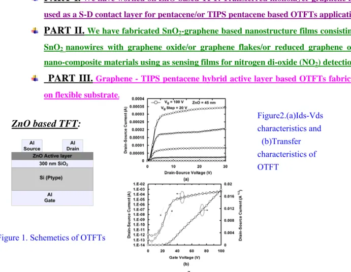
Figure2.(a)Ids-Vds characteristics and (b)Transfer characteristics of OTFTEnhancement-mode zinc oxide (ZnO) channel thin film transistors (TFT) shown in Fig. 1, were fabricated on commercially available SiO2/p-Si substrate from layers deposited at room temperature using rf magnetron sputtering. The ZnO channel thicknesses have been optimized with bottom gate TFT. The effects of different channel thickness on the structural and pulse measurements of ZnO TFTs were examined. As the channel thickness increased, the crystalline quality and the channel conductance become enhanced. The optimized ZnO TFT exhibited enhancement mode characteristics with the drain current on-to-off ratio was varied from ~ 108 and the maximum field effect mobility varied from 8.36 to16.40 cm2V-1s-1 for ZnO thickness of 45nm, and 70 nm respectively. Figure 2(a) shows the IDS-VDS characteristics of TFT transistors (45 nm thick ZnO channel layer) with 300-nm-thick SiO2 gate dielectric. The gate voltage Vgs is varied from 0V to 100 V.
Introduction
Graphene, a two dimensional single atomic layer of hexagonally packed honeycomb lattice carbon atoms, has drawn significant attention with its outstanding electrical, mechanical, and chemical properties. This is due to extraordinary strength of the carbon bond and the availability of free π-electrons in the graphitic configuration, exceptionally high carrier mobility up to 200,000 cm2V-1s-1, where as Silicon has mobility of 100~1000 cm2V-1s-1. New physics has been predicted and observed suchas ultrathin carrier mobility, electron hole symmetry,quantum Hall effect and the suppression of weak localization. Various promising applications based on graphene have been demonstrated, such as electronics, optoelectronics, and chemical and biological sensing.
PART I.
Graphene-based electrodes for Enhanced Organic Thin Film Transistors based
on Pentacene. We summarize the last 1 yr research briefly
(Project awarded fromNational Science Council (NSC, Taiwan) in the year of 2011. Project title: "Investigation of
Graphene as ultrathin patterned transparent electrode for organic field effect transistors on large area using solution-process, as flexible electronic semiconducting material for ultra thin film transistor, and as gas sensor based on graphene- nanomaterials", Project No:
National Science Council of Taiwan under contracts NSC A1011-0815 (101-2218-E-006-006)
(duration:101/06/01 ~ 102/05/31) of Tainan, 701 Taiwan.
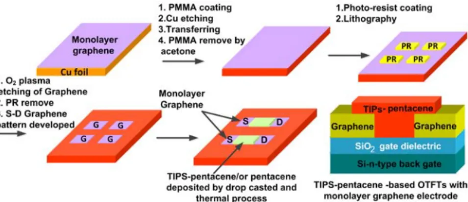
Graphene Transferr process by PMMA supported method OTFT fabrication process
Typical SEM images of transferred graphene film on SiO2/Si substrate
AFM images of the transferred graphene film and AFM images of 65 nm-thick pentacene films at the interface between the bare SiO2 surface and a graphene
S-D electrode
Raman spectra of the monolayer graphene film transferred from the CVD growth Cu foil to the SiO2/Si substrate and Raman spectra of the patterned monolayer
graphene S-D electrode after conventional lithography/O2 plasma reactive ion
The results of XRD spectroscopy of Pentacene and TIPS pentacene semiconductor layers.
Channel width-normalized Rtotal (contact resistance ) of pentacene OTFTs with
Au electrodes and graphene electrodes.
Electrical properties of TIPS-pentacene/or pentacene with monolayer graphene as well as Au electrodes OTFTs.
FIB and HR-TEM image of pentacene deposited on the interface between the graphene electrode and the SiO2 surface
Graphene based S-D OTFTs reliability test after 6 month.
Figure 3. (a) Complete schematic of the fabrication steps of bottom-gate, bottom-contact TIPS-pentacene OTFTs with
monolayer graphene S-D electrodes on an SiO2 (300 nm)/Si substrate. TIPS-pentacene was drop-casted via the solution
process. The device dimension is W/L = 1500 μm/150 μm.
The electrical characteristics of the patterned graphene electrodes for organic devices were investigated using a series of pentacene and 6, 13-bis (triisopropylsilylethynyl) pentacene (TIPS-pentacene)-based OTFTs with bottom-contact geometry fabricated on an n-doped (resistivity of ~0.001 ohm/cm to 0.006 ohm/cm, back gate) Si wafer with a 300 nm SiO2 dielectric layer. Device performance was then compared with conventional Au-based OTFTs. The TIPS-pentacene and 65 nm-thick pentacene films were deposited via drop-casting and vacuum-assisted thermal evaporation, respectively.
The optical and scanning electron microscopy (SEM) images of a graphene film on an Si/SiO2 substrate transferred by traditional PMMA-supported method was thoroughly examined to evaluate the quality of the film.The growth of pentacene on the graphene electrode, the channel region, and their excellent interface compatibility were clearly observed through high-resolution transmission electron microscopy (HRTEM) and SEM analyses.
All measurements were obtained under atmospheric conditions at room temperature. The dielectric properties of the metal–insulator–metal structure were investigated using an HP 4284 C-V plotter. The electrical characteristics of the devices were analyzed with a semiconductor parameter analyzer
(Agilent B1500A, CA, USA).The surface morphology of the graphene film on SiO2/Si substrate transferred by conventional PMMA-assisted method were monitored using a high-resolution thermal field-emission scanning electron microscope (FE-SEM, JEOL, JSM-7001). Atomic force microscopy (AFM) images were obtained through the contact mode of a scanning probe microscope. Raman measurement was performed on a Jobin Yvon LabRam HR spectroscope.
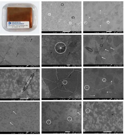
Figure 4.Typical SEM images of graphene film on SiO2/Si substrate transferred by conventional PMMA-assisted method.
Residual metal particles (white circles), small holes (black circles), nanometer-width wrinkles (white solid lines), and small folds or gaps (black dotted arrows) that formed as a result of incomplete contact between the PMMA/graphene stack and the target substrate could be observed. Several multilayer graphene areas (darker contrast was marked by white dotted arrows). Long cracks were also found when samples were handled with Teflon tweezers before Cu etching, as indicated by the black oval circle on the left side. These measurements were conducted on different transferred samples. The scale bars used were in 10 μm, 1μm, and 100 nm levels.
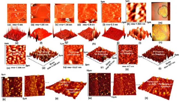
Figure 5. The 2D tapping mode of the AFM images of the transferred graphene film on SiO2/Si substrate with scanning
ranges of (a) 15 μm, (b) 10 μm, (c) 5 μm, and (d) 2.5 μm. (e), (f), (g), and (h) illustrate the corresponding 3D images. (i) 2D and (j) 3D AFM images of TIPS-pentacene deposited on graphene S-D electrode. (k) 2D and (l) 3D AFM images of TIPS-pentacene deposited on SiO2 layer. (m) Optical microscopy image of TIPS-pentacene drop-casted via the solution
process on patterned graphene S-D electrodes. (n) Enlarged view of image (m). AFM images (2 μm × 2 μm), (o) and (p) respectively show the 2D and 3D images of a 65 nm-thick pentacene film thermally grown on bare SiO2 layer. (q) and (s)
show the 2D, and (r) and (t) show the 3D images of pentacene films thermally grown on graphene S-D electrodes. The pentacene film grown on graphene S-D electrodes has different roughness and grain sizes because of the presence of PMMA residues (white spots) on graphene during the transfer of graphene from the Cu foil through PMMA support. 2D [(u) and (w)] and 3D [(v) and (x)] AFM images of 65 nm-thick pentacene films at the interface between the bare SiO2
PART-II
SnO
2-GO based nanostructures film for NO
2gas detection
Motivation and Advantages of SnO2-graphene-based nanostructure films
FTIR and XRD study of different SnO2-graphene-based nanostructure films
Raman analysis XPS study
Surface morphology study through FE-SEM and HR-TEM Gas response mechanism
Sensitivity and response curve of resistive SnO2-graphene-based resistative sensor.
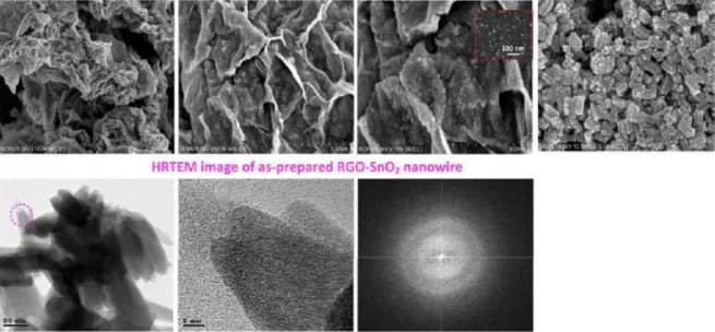
Figure 7. Surface Morphology and HR-TEM images of RGO-SnO2 nanoparticle and nanorod composites. The as-prepared
RGO-SnO2 composites indicate amorphous nature. Annealing at 500 oC showing polycrystalline characteristics. The
nanoparticles almost ~10 nm in size are uniformly distributed on reduced graphene surface.
Sensitivity and transient response curve
Figure 8. Sensitivity and transient response curve
F-doped SnO
2for Gas sensor application:
Pure and Fluorine-modified tin oxide (SnO2) thin films (250~300 nm) have been uniformly deposited on corning glass substrate by sol-gel technique to fabricate SnO2 based resistive sensor for ethanol detection. It has also been observed that the F-doped SnO2 films have a lower resistivity (0.12x 10⁻⁴ Ω-cm) in comparison with pure (14.16x10⁻⁴ Ω-cm) one.Here we are presenting 3 different composite films of GF-3-SnO2, GO-SnO2-10h and RGO-SnO2 hybrid
resistative sensor. The
The SnO2-RGO sensor exhibited two times more
sensitivity (S~9600) as compare to SnO2-GF-3-SnO2
(S~4975) sensor. The improvement of sensitivity could be attributed due to the less oxygen functionalized SnO2
nanowires and higher surface area of SnO2-RGO
composite.
The sensing mechanism of SnO2-GO composite films
depends on the interface between GO nano-grains and SnO2 nanowires.43,44
The sensitivity increases with the concentration of NO2
gas, as example SnO2-3-SnO2 showing sensitivity of
4620, 2500 and 1900 at different ppm of 8, 4 and 2, respectively.
X-ray diffraction (XRD) and scanning electron microscopy (SEM) techniques were used to analyze the structure and the surface morphology of the prepared films. The resistance change was studied at different temperatures (523~623K) with metallic contacts of silver in air and in the presence of different concentrations of ethanol vapour. Comparative gas sensing results reveal that the prepared F-doped SnO2 sensor exhibited lowest response time and recovery time of 10s and 13s, respectively. In the case of pure SnO2 gas sensor these values were 32s and 65s, respectively. The maximum sensitivities of both gas sensors were obtained at 623K. Figure 3 shows the transient response curves, where the change of resistance value plotted with time. The 1250 ppm ethanol gas vapour was injected at 623K and then flushed off immediately (a) Pure SnO2, (b) F-doped SnO2, and (c) comparison of sensitivity for Pure and F-doped SnO2 gas sensor. Figure 4 sows the Sensitivity, response time, and recovery time as a function of temperature for (a) Pure and (b) F-doped SnO2 sensor.
Figure 10. Sensitivity, response time, and recovery time (a) F-doped SnO2 (b) Pure SnO2.
Figure 9. The change of resistance value plotted with time.
(a) Pure SnO2, (b) F-doped SnO2, and (c) comparison of sensitivity (b) for Pure and F-doped SnO2 gas sensor.
PART -III
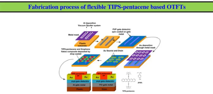
6, 13-bis(triisopropylsilylethynyl) pentacene–graphene composite layers for flexible thin-film transistors with a polymer gate dielectric
Solution processible poly(4-vinylphenol) as the transistor dielectric material for low-cost processing on flexible substrates at low temperatures is employed. A 6,13-bis (triisopropylsilylethynyl) (TIPS) pentacene–graphene hybrid semiconductor is drop casted to fabricate bottom-gate and bottom-contact field effect transistor devices on flexible and glass substrates under ambient air environment. A few layers of graphene flakes increased the area in the conduction channel, and forming bridge connection between the crystalline regions of the semiconductor layer which can change the surface morphology of TIPs pentacene films. The TIPS pentacene–graphene hybrid semiconductor-based organic thin film transistors (OTFTs) cross-linked with poly(4-vinylphenol) gate dielectric exhibit an effective field-effect mobility of 0.076 cm2V-1s-1 and a threshold voltage of -0.7 V at Vgs = -40 V. By contrast,
typical TIPS pentacene shows four times lower mobility of 0.019 cm2V-1s-1 and threshold voltage of 5 V. The grapheme/TIPS pentacene hybrids presented in this paper can enhance the electrical characteristics of OTFTs due to their high crystallinity, uniform large grain distribution, and effective reduction of crystal misorientation of the organic semiconductor layer, as confirmed by X-ray diffraction spectroscopy, atomic force microscopy, and optical microscopy studies.
Fabrication process of flexible TIPS-pentacene based OTFTs
Fig. 11 Schmetics illustration of the device fabrication steps, the cross-sectional schematics of the TIPS
pentacene–graphene-based TFTs fabricated on plastic substrate and glass substrate. The chemical structure of TIPS pentacene and PVP gate dielectric are also shown. The thickness of the cross-linked PVP layer was 650 nm, as measured by the alpha step.
Electrical characteristics of OTFTs
Fig.12. Output characteristic curves of (a) TIPS pentacene–graphene hybrid OTFTs and (b) TIPS pentacene OTFTS on
plastic substrate. Gate voltage was varied from 10 V to -60 V in steps of -5 V. The transfer curves of (c) TIPS pentacene–graphene hybrid OTFTs and (d) TIPS pentacene OTFTS. This device was fabricated on PVP/Al/plastic substrate.The gate leakage current (Ig, A) versus gate –source voltage (Vgs) were plotted in Fig. 8.(d). The threshold voltage
(VT) of TIPS pentacene–graphene hybrid OTFTs is -0.7 V lowers than that of the pure TIPS pentacene OTFTs (5 V)
Fig. 13.HRTEM images of a graphene flakes disperse in tetralin solvent with different concentrations, (a, b, c) 5mg/5ml, (d, e)10mg/5ml, (f, g, h, I, j) 15mg/5ml, and (k, l, m) 20 mg/5ml. High- resolution imaging of the clear folded edge indicating single layer to few layers graphene film.
Graphene based back gate FETand AFM images of single layer and multilayred
graphene
(a)We have prepared graphene oxide by Hummer’s method and did XPS, XRD, Raman, FTIR AFM characterization.
(b) We transfer single layer graphene from CVD growth Cu foil by Cu foil etching. We have prepared back gate FET device
Fig.14. (a) Back gate graphene FET, SiO2/Si (P-type) (gate length ~3 um, Vgs~ -80 V to 10V). AFM images of transferred (b) single layered (c) multi layered graphene films on SiO2 surface
Graphene Oxide and TiO
2, SnO
2, Plladium, Gold, Silver nanowire/nanoparticle
0.00E+003.00E-02 6.00E-02 9.00E-02
composite films used for supercapacitor application.
Figure 15. Graphene oxide SnO2 nanorod prepared at different temperature by hydrothermal process (morphology controlled through different reaction condition)
Figure 16. Graphene oxide TiO2 composite nanorod
Figure 17. Reduced GO-Palladium, Graphene flakes-palladium, graphene oxide- palladium nanorod
tructure
Figure 18. TEM images of Graphene-gold nanostructure
5 1/nm 5 nm
Figure 19. TEM images of Graphene-silver nanostructure
Conclusion:
1. Here we have discussed briefly the quality of transferred monolayer graphene film used as S-D electrode for pentacene and TIPS-pentacene based OTFTs. Very systematical study of surface morphology, roughness, interface property, the degree of crystallinity, electrical characteristics have been demonstrated here.
2. In this present study, efforts have been ongoing to focus on the effects of morphology, reduction degree, and device fabrication of graphene-SnO2 composites on selectivity, sensitivity, and recovery properties of detector devices by following the simple hydrothermal process. The length (~30 μm) diameter (~70nm) and surface morphology can be easily tuned by choosing the precursor material and varying the concentration and reaction time. In a typical procedure, the alkoxide was transformed into a chain-like, glycolate complex that subsequently crystallized into uniform SnO2-GO composite nanowires. The SnO2-RGO nanowire array structures exhibited excellent response to target gases at 50 oC temperature (detection limit of 2 ppm for NO2) in comparison with SnO2-graphene flakes, GO-SnO2 nanoparticles and pure SnO2-based sensors. We strongly believe that different morphological nanostructured SnO2/graphene-based materials will open new opportunities for improving sensitivity as well as selectivity for gas sensor applications. The screening of different gas sensing (NH3, H2S) studies is under progress.
3. Organic thin film transistors based on a composite semiconductor layer from a TIPS pentacene solution blended with a graphene nanoflake powder have been fabricated, which could enhance the mobility of OTFTs as compared to conventional OTFTs. The demonstrated efficient low-temperature solution-based fabrication process could provide new insights for application in novel, low-cost, and large-area electronics on flexible substrates.
Future pending work
Synthesis for graphene nanoribbons by chemical route Graphene nanomesh as a active material for semiconductor devices. (We would like to investigate graphene nanomesh as active semiconducting layer for TFT device. Graphene nanomesh (continuous semiconducting film) can effectively introduce lateral quantum
confinement in a large piece of graphene to fine-tune the band gap for room temperature transistor operation). The nanomeshes are prepared using block copolymer lithography and can have variable periodicities including neck widths as low as 5 nm. The formation of graphene nanoribbons and nanomesh allows opening of conduction band gaps with tunable electronic properties.
InGaZnO, HfInZnO as active materials by solution process
OTFTs based on graphene S-D electrode on flexible plastic substrate
Optimize the transferring process. Need to improve the quality of transferred graphene film. Fictionalization of graphene.
Writing paper for SnO2-Graphene based hybrid gas sensor List Of Papers
1. S. Basu, P. K. Singh, J. J. Wang, and Y.-H. Wang*, “Liquid phase deposition of Al2O3 thin
films on GaN,” J. Electrochem. Soc., 154 (12) H1041-H1046, 2007.
2. S. Basu, P. K. Singh, P. W. Sze, and Y.-H. Wang*, “AlGaAs/InGaAs metal-oxide-semiconductor pseudomorphic high electron mobility transistor with low temperature liquid phase deposited Al2O3 gate insulator,” J. Appl. Phys., 104, 054116-1 to 7,
2008.
3. S. Basu, P. K. Singh, P. W. Sze, and Y.-H. Wang*, “Al0.2Ga0.8As/In0.15Ga0.85As MOS-PHEMT
with low temperature LPD-deposited Al2O3 as gate dielectric,” Solid State Electronics, vol 54,
pp. 763-768, 2010.
4. S. Basu, P. K. Singh, P. W. Sze, and Y.-H. Wang*, “AlGaN/GaN metal-oxide-semiconductor high electron mobility transistor with liquid phase deposited Al2O3 as gate dielectric,” J. Electrochem. Soc., 157 (10), 2010, H947-H951.
5. S. Basu, P. K. Singh, S. K. Lin, P. W. Sze, and Y.-H. Wang*, “Effects of Short-term DC Bias Induced Stress on n-GaN/AlGaN/GaN MOSHEMT with a Liquid Phase Deposited Al2O3 as
Gate Dielectric,” IEEE Trans Electron Devices, Nov 2010, 57(11), Nov 2010, 2978-2987. 6. Sarbani Basu(石善怡), Pramod K. Singh, C Ghanshyam, Pawan Kapur and Yeong Her Wang,
"Active layer thickness effects on the on-state current and the pulse measurement of room temperature deposited Zinc oxide thin film transistors" Journal of Electronics material, Vol. 41, No. 9, 2012, 2362-2368.
7. Sarbani Basu, Mu Chen Lee and Yeong-Her Wang, “Graphene-based electrodes for Organic Thin Film Transistors: Graphene transfer, surface morphology and interface properties of Pentacene films on Graphene/SiO2 surface” submitted to Phys. Chem.Chem.Phys, (under review, 2013).
8. Sabani Basu, Feri Adriyanto and Yeong-Her Wang "Fabrication of flexible 6, 13-bis(triisopropylsilylethynyl) pentacene-graphene composite thin-film transistors with a polymer gate dielectric,"Nanotechnology (accepted 2013).
9. Sarbani Basu, and Yeong-Her Wang "P3HT-ZnO composite layer enhancing the mobility of organic thin film transistors" (under preparation)
10. Sarbani Basu, and Yeong-Her Wang SnO2-graphene nanostructured material towards NO2 and H2S gas sensing (under preparation).
11. Sarbani Basu and Yeong-Her Wang “Monolayer patterned graphene as source-drain electrodes for bottom contact organic field effect transistors” Nov. 2013 IEDMS, Nantau, Taiwan (Best poster paper award)
12. S. Basu and C. Ghanshyam, “The Electrical and material characterization of liquid phase deposited Al2O3 thin film on Gallium nitride (GaN) substrate,” National conference on new horizons in Avionics Display system, NHADS 2010, CSIO, Chandigarh, India, 23 Oct, 2010.
13. S. Basu, Y. H. Wang*, C. Ghanshyam, and P. Kapur, “Fast response time alcohol gas sensor using nanocrystalline F-doped SnO2 films derived via sol-gel method,” Forthcoming articles,
Bulletin of Materials Science, Vol. 35, 2012.
14. S. Basu, and Yeong-HerWang, “Ethylene glycol mediated synthesis of graphene oxide and tin oxide-based nanocomposites for highly sensitive NO2 detection,” IEEE-Nanotechnology