行政院國家科學委員會專題研究計畫 成果報告
子計畫四:大晶粒低溫多晶矽膜之製程設計暨膜質分析與系 統評估
計畫類別: 整合型計畫
計畫編號: NSC93-2218-E-011-006-
執行期間: 93 年 08 月 01 日至 94 年 07 月 31 日 執行單位: 國立臺灣科技大學電子工程系
計畫主持人: 葉文昌
計畫參與人員: 陳國照, 李昇儒, 柯敦元, 黃祥恩
報告類型: 精簡報告
報告附件: 出席國際會議研究心得報告及發表論文 處理方式: 本計畫可公開查詢
中 華 民 國 94 年 10 月 31 日
行政院國家科學委員會補助專題研究計畫 V 成 果 報 告
□期中進度報告 以準分子雷射製造大晶粒低溫多晶矽膜設備研發 子計畫四:大晶粒低溫多晶矽膜之製程設計暨膜質分
析與系統評估
計畫類別:□ 個別型計畫 V 整合型計畫 計畫編號:NSC 93-2218-E-011-006-
執行期間: 93 年 8 月 1 日至 94 年 7 月 31 日
計畫主持人:葉文昌 共同主持人:
計畫參與人員: 陳國照,柯敦元,黃祥恩,李昇儒
成果報告類型(依經費核定清單規定繳交):V 精簡報告 □完整報告
本成果報告包括以下應繳交之附件:
□赴國外出差或研習心得報告一份
□赴大陸地區出差或研習心得報告一份
V 出席國際學術會議心得報告及發表之論文各一份
□國際合作研究計畫國外研究報告書一份
處理方式:除產學合作研究計畫、提升產業技術及人才培育研究計畫、
列管計畫及下列情形者外,得立即公開查詢
□涉及專利或其他智慧財產權,□一年□二年後可公開查詢 執行單位:台灣科技大學
中 華 民 國 94 年 10 月 30 日
附件一
*Invited paper on 1st Int’l TFT Conference, Kyung-Hee Univ., Soel, Korea, 3/2005
Remarkable enlargement of excimer-laser induced lateral grain by photosensitive heat retaining layer
Wenchang Yeh
Nat’l Taiwan Univ. of Sci. &Tech., No.43, Sec. 4, Keelung, Rd, Taipei106, Taiwan Tel: +886-2-27376375, Email: [email protected]
中文摘要
結晶粒俓是關係TFT特性很大的因素,長久以來即被研究以提高基板溫度,增長雷射 脈衝延續時間等方式增長粒徑,但始終只能得到增長2倍左右之效果。本研究開發出半透光 熱滯留輔助層以替代傳統基板結構中 矽膜/阻擋層/基板之阻擋層,而以此結構在對矽膜進 行準分子雷射退火時成功地使矽膜結晶粒大小增大了10倍(與傳統方式比較下),達到平均10 微米直徑之結晶粒。以本研究中所架設之即時矽膜反射率穿透率監控得知,此方式中之矽 膜溶化時間由於半透光熱滯留輔助層之存在而由傳統方式中之60ns增長了10倍,達到 500ns。此結果與本研究中理論計算之結果相符。
Abstract
Photosensitive capping or under layer as the heat retaining layer(HRL) of Si film in ELA will be shown theoretically and experimentally to be effective on enhancement of grain growth.
The diameter of disc grains in the SLG regime for 100nm Si film under room temperature ELA was enlarged dramatically to 10μm. Time-resolved optical transmittance revealed that the melt duration has been increased from 60ns to 500ns in this study for the first time. In application of the HRL, a new method for lateral grain control is demonstrated with no new laser annealing system, no precise alignment between the 1st TFT mask and lateral grain, and no additional photolithographic process.
KEYWORD:
Thin-Film Transistors, Poly-Si, Excimer Laser, photosensitive heat retaining layer 薄膜電晶體,多晶矽,準分子雷射,熱滯留輔助層
1. Introduction
TFTs with higher mobility and uniformity are demanded for next-generation “system displays”. The electrical characteristics of poly-Si TFT such as mobility, threshold voltage and the uniformity are closely related to grain size of poly-Si film. However, the grain sizes of the poly-Si film fabricated by conventional excimer laser annealing(ELA) method are under 1 μm and therefore not enough.
In order to fabricate high performance TFTs, TFTs with no grain boundaries perpendicular to the carrier drift direction are demanded. This can be realized by both grain enlargement and grain control. Grain enlargement can be achieved by applying the lateral grain or increasing the melt duration of Si film in ELA. The grain control, which generally means the control of lateral grain, can be achieved by inducing lateral temperature gradient in a molten a-Si film. Several methods have been proposed and realized for inducing lateral temperature gradient in a melted a-Si film, for example, by modulation of laser intensity such as in PMELAi (phase modulated ELA) or SLSii(sequential lateral solidification) methods, or by modulation of Si film thickness such as in micro-Cziii or recessed structure methodiv.
As for the grain enlargement, the generally used method is thickening of the Si film, and rising of the substrate temperaturev,vi to elongate the melt duration. Elongating the melt duration not only enhances the grain growth, but also enhances the crystalinity due to nearer equilibrium grain growth. Therefore, elongating the melt duration will be still important even for the advanced generation TFT with a shorter channel length. However the effects are still limited due to limitations on the Si film thickness and a tolerant temperature of glass in above methods. SiO2
film can capped on the Si film instead of thickening the Si film, however, capping layer with more than 400nm inversely work as heat sink to shorten the melt duration. Recently, photosensitive layer as the capping layer of Si film in PMELA method was proposed by W. Yeh and M. Matsumura, and dramatic elongation of lateral grains to 60μm have been achievedvii. After that, we proposed using photosensitive film as the under layer of Si film with irradiating the laser light from the back side of glass substrateviii. As a
result, disk grains with the diameter of as large as 10μm in SLG regime was achieved even at room temperature ELA. Therefore the photosensitive layer is a simple and promising method for enhancing the grain growth. In this paper, our recent results on excimer-laser induced lateral grain with photosensitive heat retaining layer will be demonstratedix,x.
2. Theoretical analysis of the effect of photosensitive heat retaining under layer on grain growth enhancement
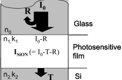
Figure 1 shows the laser light rays in the Si/SiOxNy/glass sample structure. The pulse laser R I0
T
ISiON(= I0-T-R) Photosensitive film
Si Glass n0
n1,k1
n2,k2
I0-R
Fig. 1 laser lays in sample structure
R I0
T
ISiON(= I0-T-R) Photosensitive film
Si Glass n0
n1,k1
n2,k2
I0-R
R I0
T
ISiON(= I0-T-R) Photosensitive film
Si Glass n0
n1,k1
n2,k2
I0-R
Fig. 1 laser lays in sample structure
energy density (J/cm2) I0 was irradiated from the back side of glass substrate. The photosensitive film absorbs a part of laser energy to rise temperature itself, so Si film can keep molten for a longer time due to a loosen temperature gradient at the Si/substrate interface. This effect on enhancing the grain growth is similar to substrate heating effect, but is more effective because the temperature of photosensitive layer can be higher than the soften temperature of glass. In this section we will calculate the laser energy absorbed by photosensitive layer during excimer laser annealing of Si film in this method.
In fig.1 reflectivity of about 4% at the glass surface and the phase of light were neglected for simplicity. R is the effective reflected laser energy density (J/cm2) at the back surface of photosensitive film and T is the effective transmitted laser energy density(J/cm2) in Si film. R and T can be shown by
) 1 exp (
1
exp ) 1 )(
1 (
2 2 1
0 2 1
d d
r r
I r
T r -a a
-
- -
= -
) 2 exp (
1
exp ) 1 (
2 2 1
2 0 2 2 1 0
1 d
d
r r
I r I r
r
R a
a -
-
- + -
=
where r1 is the reflectivity between glass and the photosensitive film, r2 the reflectivity between the photosensitive film and the silicon, α the absorption coefficient of photosensitive film, and d the film thickness of photosensitive film. r1 and r2 can be calculated from the optical constant of these materials. 800nm and 2 were taking for the thickness and refractive index of SiOxNy photosensitive film. And the energy conservation equation
I0 = R + Ision + T (4)
where Ision is the energy density absorbed by SiOxNy photosensitive layer. The more Ision it absorbed, the higher its temperature will be raised, and therefore the longer the melt duration.
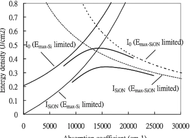
However, a limitation arose from the critical absorbable volume energy density Emax-Si and Emax-SiON (J/cm3) for the Si and the photosensitive film, respectively. Emax-SiON can be estimated experimentally and were about 8300J/cm3 from our result. As for Emax-Si, since Tmax = Emax-Si/αSi, Tmax is used in calculation instead of Emax-Si for convenient. 0.14J/cm2 is estimated for Tmax from the ablation energy of the Si film without
photosensitive layer (reflectivity of 0.42 had been considerate). Based on these two limitations on Tmax and Emax-SiON, the I0 and Ision as functions of αsion can be obtained from relating eq(1), eq(2) and eq(3). The results are shown in Fig. 2. The dotted lines are the I0 and Ision under a limitation without destruction of photosensitive layer, and the solid lines are I0 and Ision under a limitation without ablation of Si layer. When the
Fig. 2 Laser energy density as functions on absorption coefficient
0 0.1 0.2 0.3 0.4 0.5 0.6 0.7 0.8
0 5000 10000 15000 20000 25000 30000 Absorption coefficient (cm-1)
Energy density (J/cm2)
I0 (Emax-SiON limited)
ISiON (Emax-SiON limited) I0 (Emax-Si limited)
ISiON (Emax-Si limited)
Fig. 2 Laser energy density as functions on absorption coefficient
0 0.1 0.2 0.3 0.4 0.5 0.6 0.7 0.8
0 5000 10000 15000 20000 25000 30000 Absorption coefficient (cm-1)
Energy density (J/cm2)
I0 (Emax-SiON limited)
ISiON (Emax-SiON limited) I0 (Emax-Si limited)
ISiON (Emax-Si limited)
absorption coefficient α is increased from 0 to 13500cm-1, the larger the α is, the larger Ision. It has a maximum value at around 13500cm-1, and then decreased with increasing the α. Therefore, the optimized αsion for best enhancement effect on grain growth is around 13500cm-1 for 800nm-thick photosensitive layer. This result agrees well with our experimental result.
3. Experiments on photosensitive layer enhanced grain growth
Sample structure in experiment is shown in Fig.3. Corning 7059 was used as the substrate, and then SiONx film as the photosensitive film was deposited by PECVD using trimethylsilane(TMS), O2 and N2 gas. SiO2 was used as buffer film which was successively deposited on photosensitive film. The a-Si film was then deposited on SiO2 by sputtering at 200oC. Then 1 pulse of XeF excimer laser light was applied from backside of glass substrate at room temperature.
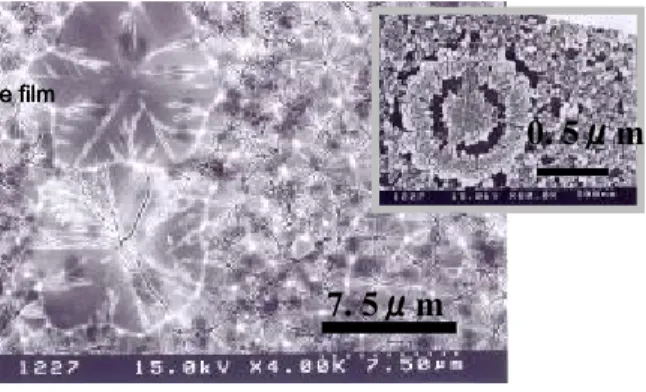
Figure 4 shows the SEM image of Disk grain in SLG regime with (α=12000cm-1) and without (α=0cm-1) photosensitive film after Secco’s etching. The diameter of the disk grain at SLG regime is remarkably enhanced from 0.8μm to 10μm with photosensitive film.
Figure 5 shows the grain sizes and the critical laser energy densities of crystallization Ec, completely melt Em and ablation Ea as functions of absorption coefficient of photosensitive layer.
7. 5μm
Fig. 4 disc grain with α= 12000 (left) & 0 cm-1 0. 5μm
7. 5μm
Fig. 4 disc grain with α= 12000 (left) & 0 cm-1 0. 5μm
Fig.5 Grain sizes and critical laser energy densities as functions of absorption coefficient
0 50 100 150 200 250 300 350
0 2000 4000 6000 8000 10000
Absorption coefficient (cm-1)
Laser energy density (mJ/cm2)
0 1 2 3 4 5 6 7 8 9 10
Grain size (micorn)
a-Si Partially melt Completely melt
Fig.5 Grain sizes and critical laser energy densities as functions of absorption coefficient
0 50 100 150 200 250 300 350
0 2000 4000 6000 8000 10000
Absorption coefficient (cm-1)
Laser energy density (mJ/cm2)
0 1 2 3 4 5 6 7 8 9 10
Grain size (micorn)
a-Si Partially melt Completely melt
1.00E-08 1.00E-07 1.00E-06 1.00E-05
Time (s)
Tranmittance (arb. lenear unit)
Nucleation time = 500ns 60ns
450
300 325 275
250 225
200
180 with α =0 120with α =0
Fig. 6 Time-resolved optical transmittance spectra depends on laser energy density(mJ/cm2)
1.00E-08 1.00E-07 1.00E-06 1.00E-05
Time (s)
Tranmittance (arb. lenear unit)
Nucleation time = 500ns 60ns
450
300 325 275
250 225
200
180 with α =0 120with α =0
Fig. 6 Time-resolved optical transmittance spectra depends on laser energy density(mJ/cm2) XeF excimer laser
FWHM: 25ns He-Ne laser
Filter
Photo detector
Under construction
Under construction
Corning 7059
800nm SiOxNy photosensitive film 100nm SiO2 buffer film
90nm Sputter a-Si film
Figure3. sample structure and Time-resolved optical transmittance system
XeF excimer laser FWHM: 25ns He-Ne laser
Filter
Photo detector
Under construction
Under construction
Corning 7059
800nm SiOxNy photosensitive film 100nm SiO2 buffer film
90nm Sputter a-Si film XeF excimer laser
FWHM: 25ns He-Ne laser
Filter
Photo detector
Under construction
Under construction
Corning 7059
800nm SiOxNy photosensitive film 100nm SiO2 buffer film
90nm Sputter a-Si film
Figure3. sample structure and Time-resolved optical transmittance system
Ec, Em and Ea all increased in the sample with α = 900cm-1. This shows a part of laser light energy is absorbed by photosensitive layer, as have shown in previous section.
4. Transient transmissivity measurement of Si film during laser exposure
The crystallization processes were monitored in situ and in real time by measuring the time resolved transmission of a He-Ne 633nm laser through the center of the spot irradiated by the XeF excimer laser, as shown in Fig3. The excimer laser light was incident from backside of glass substrate to pass through photosensitive film into the Si film. The substrate temperature was kept at room temperature. Figure 6 shows the transient transmission for irradiation of different laser intensities with and without the photosensitive under layer. Upon exposure, the transmission decreased dramatically to a minimum. This is due to the high reflectivity of molten Si at film surface since the liquid Si has metal-like optical properties. After the transmission have reached a minimum, it increased immediately without time delay in the under complete melting regime(I ≤ 300mJ for α = 9000cm-1 and I ≤ 160mJ for α = 0cm-1). This means the solidification occurred immediately after laser irradiation. This is likely due to either explosive crystallization or crystallization from the unmolten Si at surface. The gradient of the transmission curve during solidification, therefore, can be related to the solidification rate. As for the complete melting regime (I > 300mJ for α = 9000cm-1 and I > 160mJ for α = 0cm-1), there appeared an incubation time for solidification. This is the time delay for occurrence of nucleation, or so called melt duration. This is important for lateral growth because the lateral grain keep growing until nucleationxi. In this study, the melt duration is 500ns for α = 9000cm-1 and 60ns for α = 0cm-1. Therefore the grain growth can be enhanced dramatically for the Si film with photosensitive layer.
5. Location control of lateral grain
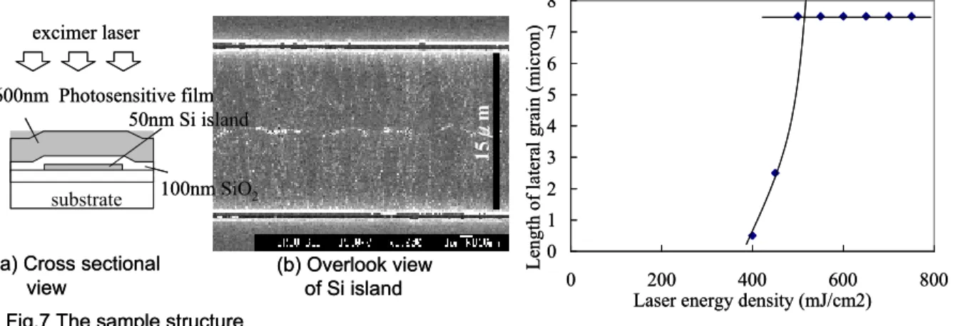
Location control of lateral grain is necessary for fabrication of TFT. There are many methods proposed for excimer laser induced lateral growth. We have proposed HREC(heat retaining layer enhanced crystallization) method where pre-patterned Si islands for TFT are capped with the
0 1 2 3 4 5 6 7 8
0 200 400 600 800
Laser energy density (mJ/cm2)
Length of lateral grain (micron)
Fig. 8 lateral grain length depends on laser energy density
0 1 2 3 4 5 6 7 8
0 200 400 600 800
Laser energy density (mJ/cm2)
Length of lateral grain (micron)
Fig. 8 lateral grain length depends on laser energy density
15μm
excimer laser
50nm Si island 100nm SiO2 600nm Photosensitive film
substrate
Fig.7 The sample structure
and SEM image of crystallized Si island (a) Cross sectional
view (b) Overlook view
of Si island
15μm
excimer laser
50nm Si island 100nm SiO2 600nm Photosensitive film
substrate
Fig.7 The sample structure
and SEM image of crystallized Si island (a) Cross sectional
view (b) Overlook view
of Si island
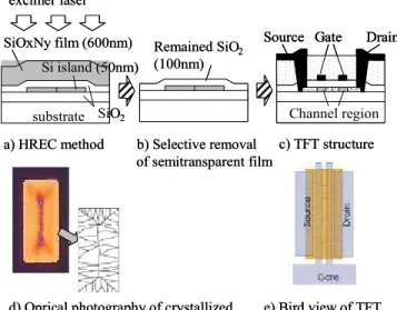
photosensitive layerxii. Figure 7 shows the structure and the SEM image of crystallized Si island after Secco’s etching. The lateral growth originated spontaneously in the edge of Si Island. In this method neither new laser annealing system, precise alignment between the 1st TFT mask and lateral grain, nor additional photolithographic processes are necessary.
Figure 8 shows the length of lateral grain in Si islands as a function of laser intensity under 1 pulse excimer laser. Lateral growth takes place at above 400mJ/cm2, and increased as increasing intensity. The length of lateral grain was saturated when the laser intensity is above 475mJ/cm2, due to the limitation on the dimension of Si islands. This is convenient for mass production because the lateral grain length is fixed to a half width of Si island. When the laser intensity is above 550mJ/cm2, holes due to ablation appeared, and the density of holes increased with increasing the intensity. The laser intensity near 750mJ/cm2 causes the condensation of the Si film from the edge of the island. After the crystallization of Si islands, the photosensitive layer on SiO2 film and Si islands was removed selectively by 85% 180oC phosphoric acid. The etching selectivity between SiOxNy photosensitive film and SiO2 film is 10xiii. Figure 9 shows the SEM images of the SiO2 capped Si island. The SiO2 surface is flat. Cavities at the center line of island is caused by impinge of the lateral grains. No cavities and cracks were observed on the surface of photosensitive film, so it seems appeared after selective etching. However, it will have few effects on the properties of TFT when the dual gate structure is applied to this island, as shown in fig.10.
Fig. 9 SEM image of the Si island with SiO2 buffer layer
25o
15μm
15o
100nm
Fig. 9 SEM image of the Si island with SiO2 buffer layer
25o
15μm
25o
15μm
15o
100nm
excimer laser
SiOxNy film (600nm)
substrate
Fig.10 HREC method and the TFT structure Gate
Source Drain
Channel region a) HREC method b) Selective removal
of semitransparent film
c) TFT structure Si island (50nm)
Remained SiO2 (100nm)
SiO2
d) Oprical photography of crystallized Si island and the lateral grain
e) Bird view of TFT excimer laser
SiOxNy film (600nm)
substrate
Fig.10 HREC method and the TFT structure Gate
Source Drain
Channel region Gate
Source Drain
Channel region a) HREC method b) Selective removal
of semitransparent film
c) TFT structure Si island (50nm)
Remained SiO2 (100nm)
SiO2
d) Oprical photography of crystallized Si island and the lateral grain
e) Bird view of TFT
6. Conclusions
Photosensitive capping or under layer as the heat retaining layer(HRL) of Si film in ELA were shown theoretically and experimentally to be effective on enhancement of grain growth. The diameter of disc grains in the SLG regime for 100nm Si film under room temperature ELA was enlarged dramatically to 10μm. Time-resolved optical transmittance revealed that the melt duration has been increased from 60ns to 500ns in this study for the first time. In application of the HRL, a new method for lateral grain control is demonstrated where uniformly distributed excimer laser light is exposed to the HRL capped pre-patterned Si islands. The lateral growth originated spontaneously in the Si islands with the length of as long as 7 micron.
REFERENCES
i CH. Oh, M. Ozawa, and M. Matsumura, Ipn. J. Appl. Phys.37(1998)L492.
ii R.S. Sposili and J. S. Im, Appl. Phys. Lett. 69(1996)2864.
iii P. Ch. van der Wilt, B.D. van Dijk, G. J. Bertens, R.Ishihara and C.I.M. Beenakker: Appl. Phys.
Lett. 72 12(2001)1819.
iv C. Cheng et al, AMLCD 2000, 281
v H. Kuriyama et. al., Jpn. J. Appl. Phys., 30(12B)1991,pp.3700-3703.
vi J.S. Im et al., Appl. Phys. Lett., 64(17)1994, pp2303-2305.
vii W.C. Yeh and M. Matsumura, Jpn. J. Appl. Phys., 41(2002) 1909
viii W.C. Yeh, AMLCD02, p153.
ix W.C. Yeh et. al., AMLCD04, p247.
x J. X. Lin et. Al., AMLCD04, p157
xi W.C. Yeh and M. Matsumura, Jpn. J. Appl. Phys. Vol. 40(2001) pp.492-499
xii W.C. Yeh et. al., AMLCD03, p159
xiii W.C. Yeh et. al., IDW04, p511.
可供推廣之研發成果資料表
□ 可申請專利 V 可技術移轉 日期:94 年 10 月 30 日
國科會補助計畫
計畫名稱:大晶粒低溫多晶矽膜之製程設計暨膜質分析與系統評估 計畫主持人:葉文昌
計畫編號:NSC 93-2218-E-011-006- 學門領域:微電子
技術/創作名稱 利用熱滯留輔助層之矽膜結晶粒增大技術
發明人/創作人 葉文昌
中文:
結晶粒俓是關係TFT 特性很大的因素,長久以來即被研究以提高
基板溫度,增長雷射脈衝延續時間等方式增長粒徑,但始終只能得
到增長2 倍左右之效果。本研究開發出半透光熱滯留輔助層以替代
傳統基板結構中 矽膜/阻擋層/基板之阻擋層,而以此結構在對矽膜
進行準分子雷射退火時成功地使矽膜結晶粒大小增大了10 倍(與傳
統方式比較下),達到平均 10 微米直徑之結晶粒。
技術說明 英文:Photosensitive capping or under layer as the heat retaining layer(HRL) of Si film in ELA will be shown theoretically and experimentally to be effective on enhancement of grain growth. The diameter of disc grains in the SLG regime for 100nm Si film under room temperature ELA was enlarged dramatically to 10μm. In application of the HRL, a new method for lateral grain control is demonstrated with no new laser annealing system, no precise alignment between the 1st TFT mask and lateral grain, and no additional photolithographic process.
可利用之產業 及可開發之產品
TFT-LCD,TFT-OLED 平面顯示器,結晶矽薄膜太陽電池
技術特點
本方式可使矽膜之準分子雷射結晶化後之結晶粒增大10 倍以上。
結晶粒俓是關係TFT 特性很大的因素,長久以來即被研究以提高
基板溫度,增長雷射脈衝延續時間等方式增長粒徑,但始終只能得
到增長2 倍左右之效果,因此本方式之效果將可期待得到良好電子
元件特性。
推廣及運用的價值
目前還需等待時機,因為此技術為次次世代技術,目前還無法受到 國內面板廠注目。但此技術已受國外,尤其日本廠商注目。趁此時 基進一步開發使技術更為成熟。
※ 1.每項研發成果請填寫一式二份,一份隨成果報告送繳本會,一份送 貴單位研 發成果推廣單位(如技術移轉中心)。
附件二